 | –≠–ª–µ–∫—Ç—Ä–æ–Ω–Ω—ã–π –∫–æ–º–ø–æ–Ω–µ–Ω—Ç: SP524CF | –°–∫–∞—á–∞—Ç—å:  PDF PDF  ZIP ZIP |

1
Rev. 7/10/03
SP522 Multi≠Mode Serial Transceivers
© Copyright 2003 Sipex Corporation
The SP522/524 is a monolithic device that supports three serial interface standards for Wide
Area Network Connectivity. The SP522/524 is ideally suited for multi-protocol designs that are
cost and space sensitive. The SP522/524 is fabricated using a low power BiCMOS process
technology. Two (2) drivers and two (2) receivers for the SP522 can be configured via software
for any of the above interface modes at any time. The SP524 offers two (2) additional drivers
and two (2) additional receivers.
SP522 -- 2 Drivers and 2 Receivers
SP524 -- 4 Drivers and 4 Receivers
Driver and Receiver Tri-State Control
Low-Cost WAN Solution
Loopback
Function for Diagnostics
Software Selectable Interface Modes:
-RS-232 (V.28), RS-423 (V.10)
-RS-422 (V.11, X.21), RS-485
DESCRIPTION
SP522/SP524
Low-Cost Programmable
Multi-Protocol Transceivers
Æ
T1IN
24
T1
T1OUTA
22
17
T2IN
25
T2
18
R1INA
44
R1OUT
43
R2OUT
T1OUTB
T2OUTA
T2OUTB
R1INB
R2INA
R2INB
LOO
PBA
CK P
A
THS
V
DD
V
DD
10
µ
F
28
V
SS
10
µ
F
+5V
V
CC
10
µ
F
14
ENT1
ENT2
ENR1
ENR2
SP524
DP0
DP1
LATCH_EN
LOOPBCK
DECODER LOGIC
40
36
35
39
20
3
4
5
6
31
32
30
23
T3IN
26
T3
T3OUTA
16
11
T4IN
27
T4
13
R3INA
42
R3OUT
41
R4OUT
T3OUTB
T4OUTA
T4OUTB
R3INB
R4INA
R4INB
LO
O
PBA
C
K P
A
THS
ENT3
ENT4
ENR3
ENR4
38
34
33
37
15
7
8
9
10
GND
12
1
21
2
19
V
SS
29
+
V
CC
V
CC
GND
GND
R2
R1
R3
R4
IN5819
T1IN
10
T1
T1OUTA
11
16
GND
14
T2IN
9
T2
15
R1INA
1
R1OUT
24
R2OUT
T1OUTB
T2OUTA
T2OUTB
R1INB
R2INA
R2INB
LO
O
P
B
A
C
K
P
A
T
H
S
V
DD
V
DD
10
µ
F
21
V
SS
V
SS
10
µ
F
22
+5V
V
CC
10
µ
F
13
+
ENT1
ENT2
ENR1
ENR2
SP522
DP0
DP1
LATCH_EN
LOOPBCK
DECODER LOGIC
5
6
4
3
12
18
17
20
19
8
7
2
23
R1
R2
1N5819

2
Rev. 7/10/03
SP522 Multi≠Mode Serial Transceivers
© Copyright 2003 Sipex Corporation
SPECIFICATIONS
Typical @ 25
∞
C and nominal supply voltages unless otherwise noted.
MIN.
TYP.
MAX.
UNITS
CONDITIONS
LOGIC INPUTS
V
IL
0.8
Volts
V
IH
2.0
Volts
LOGIC OUTPUTS
V
OL
0.4
Volts
I
OUT
= ≠3.2mA
V
OH
2.4
Volts
I
OUT
= 1.0mA
RS422 DRIVER
TTL Input Levels
V
IL
0
0.8
Volts
V
IH
2.0
Volts
Outputs
Differential Output
+2.0
+5.0
Volts
R=50
; see Figure 1
Open Circuit Voltage,V
O
+6.0
Volts
Balance
+0.4
Volts
|V
T
| ≠ |V
T
|
Offset
+3.0
Volts
Short Circuit Current
+150
mA
V
out
= 0V
Power Off Current
+100
µ
A
V
cc
= 0V, V
out
= +0.25V
Transition Time
40
nS
Rise/fall time, 10%-90%
Max. Transmission Rate
10
Mbps
R
L
=100
Propagation Delay
T
A
= +25
∞
C
t
PHL
90
150
nS
R
DIFF
=100
, Figures 3 & 5
t
PLH
90
150
nS
R
DIFF
=100
, Figures 3 & 5
RS422 RECEIVER
TTL Output Levels
V
OL
0.4
Volts
V
OH
2.4
Volts
Input
High Threshold
+0.3
+6.0
Volts
(a)-(b)
Low Threshold
-6.0
-0.3
Volts
(a)-(b)
Common Mode Range
-7.0
+7.0
Volts
High Input Current
Refer to Rec. input graph
Low Input Current
Refer to Rec. input graph
Receiver Sensitivity
+0.3
Volts
V
CM
= +7V to -7V
Input Impedance
4
k
Max. Transmission Rate
10
Mbps
Propagation Delay
T
A
= +25
∞
C
t
PHL
110
175
nS
Figures 3 & 7
t
PLH
110
175
nS
Figures 3 & 7
RS485 DRIVER
TTL Input Levels
V
IL
0.8
Volts
V
IH
2.0
Volts
Outputs
Differential Output
+1.5
+5.0
Volts
R=27
; C
L
=50pF; see Fig. 1
Open Circuit Voltage,V
O
+6.0
Volts
Balance
+0.2
Volts
|V
T
| ≠ |V
T
|
Output Current
28.0
mA
R
L
=54
Short Circuit Current
+200
mA
V
out
= ≠7V to +7V
Transition Time
40
nS
Rise/fall time, 10%-90%
Max. Transmission Rate
10
Mbps
R
L
=54
Propagation Delay
Figures 3 & 5; T
A
= +25
∞
C
t
PHL
100
150
nS
R
DIFF
=54
, C
RL
= 50pF
t
PLH
100
150
nS
R
DIFF
=54
, C
RL
= 50pF

3
Rev. 7/10/03
SP522 Multi≠Mode Serial Transceivers
© Copyright 2003 Sipex Corporation
SPECIFICATIONS
Typical @ 25
∞
C and nominal supply voltages unless otherwise noted.
MIN.
TYP.
MAX.
UNITS
CONDITIONS
RS485 RECEIVER
TTL Output Levels
V
OL
0.4
Volts
V
OH
2.4
Volts
Input
Common Mode Range
-7.0
+12.0
Volts
High Input Current
Refer to Rec. input graph
Low Input Current
Refer to Rec. input graph
Receiver Sensitivity
±
0.1
Volts
V
CM
= +12V to -7V
Input Impedance
12
k
V
CM
= +12V to -7V
Max. Transmission Rate
10
Mbps
Propagation Delay
T
A
= +25
∞
C
t
PHL
110
175
nS
Figures 3 & 7
t
PLH
110
175
nS
Figures 3 & 7
RS232 DRIVER
TTL Input Level
V
IL
0.8
Volts
V
IH
2.0
Volts
Outputs
High Level Output
+5.0
+15
Volts
R
L
=3K
, V
IN
=0.8V
Low Level Output
-15.0
-5.0
Volts
R
L
=3K
, V
IN
=2.0V
Open Circuit Voltage
-15
+15
Volts
Short Circuit Current
+100
mA
V
out
= 0V
Power Off Impedance
300
V
cc
= 0V, V
out
=
±
2.0V
Slew Rate
30
V/
µ
s
R
L
=3K
, C
L
=50pF,
between +3V to ≠3V
Transition Time
1.5
µ
s
R
L
=3K
, C
L
=2500pF
Max. Transmission Rate
120
Kbps
R
L
=3K
, C
L
=2500pF
Propagation Delay
T
A
= +25
∞
C
t
PHL
2
8
µ
S
R
L
=3K
t
PLH
2
8
µ
S
R
L
=3K
RS232 RECEIVER
TTL Output Levels
V
OL
0.4
Volts
V
OH
2.4
Volts
Input
High Threshold
1.7
3.0
Volts
Low Threshold
0.8
1.2
Volts
Receiver Open Circuit Bias
+2.0
Volts
Input Impedance
3
5
7
K
Max. Transmission Rate
120
Kbps
Propagation Delay
T
A
= +25
∞
C
t
PHL
0.2
1
µ
S
t
PLH
0.2
1
µ
S
RS423 DRIVER
TTL Input Levels
V
IL
0.8
Volts
V
IH
2.0
Volts
Output
V
DD
= +5V, V
SS
= ≠5V
High Level Output
+3.6
+6.0
Volts
R
L
=450
, V
T
= 0.9*V
OC
Low Level Output
-6.0
-3.6
Volts
R
L
=450
, V
T
= 0.9*V
OC
Open Circuit Voltage
+4.0
+6.0
Volts
Short Circuit Current
+150
mA
V
OUT
= 0V
4
Rev. 7/10/03
SP522 Multi≠Mode Serial Transceivers
© Copyright 2003 Sipex Corporation
+3.25mA
≠3.25mA
+10V
+3V
≠3V
≠10V
Maximum Input Current
versus Voltage
V.10 RECEIVER
+1.0mA
≠0.6mA
+12V
+6V
≠3V
≠7V
1 Unit Load
Maximum Input Current
versus Voltage
RS485 RECEIVER
+3.25mA
≠3.25mA
+10V
+3V
≠3V
≠10V
Maximum Input Current
versus Voltage
V.11 RECEIVER
RECEIVER INPUT GRAPHS
SPECIFICATIONS
(Continued)
Typical @ 25
∞
C and nominal supply voltages unless otherwise noted.
MIN.
TYP.
MAX.
UNITS
CONDITIONS
RS-423 DRIVER
Power Off Current
±
100
µ
A
V
CC
= 0V, V
OUT
= +0.25V
Transition Time
1.0
µ
s
Rise/fall time, 10-90%
Max. Transmission Rate
120
Kbps
R
L
=450
Propagation Delay
T
A
= +25
∞
C
t
PHL
2
8
µ
S
R
L
=450
t
PLH
2
8
µ
S
R
L
=450
RS423 RECEIVER
TTL Output Levels
V
OL
0
0.4
Volts
V
OH
2.4
Volts
Input
High Threshold
+0.3
+7.0
Volts
Low Threshold
-7.0
-0.3
Volts
Common Mode Range
-7.0
+7.0
Volts
High Input Current
Refer to Rec. input graph
Low Input Current
Refer to Rec. input graph
Receiver Sensitivity
+0.3
Volts
V
CM
= +7V to -7V
Input Impedance
4
K
V
IN
= +10V to -10V
Max. Transmission Rate
120
Kbps
Propagation Delay
T
A
= +25
∞
C
t
PHL
0.5
1
µ
S
t
PLH
0.5
1
µ
S
POWER REQUIREMENTS
V
CC
+4.75
+5.0
+5.25
Volts
V
DD
+9.5
+10.0
+10.5
Volts
V
SS
-9.5
-10.0
-10.5
Volts
I
CC
4
mA
V
CC
= +5V; DP0=DP1=0V
I
DD
10
mA
V
DD
= +10V; DP0=DP1=0V
I
SS
10
mA
V
SS
= ≠10V; DP0=DP1=0V
ENVIRONMENTAL AND MECHANICAL
Operating Temperature Range
0
+70
∞
C
Storage Temperature Range
-65
+150
∞
C
Package
24-pin SOIC, 24-pin SSOP, 44≠pin QFP

5
Rev. 7/10/03
SP522 Multi≠Mode Serial Transceivers
© Copyright 2003 Sipex Corporation
ABSOLUTE MAXIMUM RATINGS
These are stress ratings only and functional operation
of the device at these ratings or any other above those
indicated in the operation sections of the specifications
below is not implied. Exposure to absolute maximum
rating conditions for extended periods of time may
affect reliability.
V
CC
............................................................................+7V
V
DD
........................................................................+12V
V
SS
..........................................................................≠12V
Input Voltages
Logic...............................-0.5V to (V
CC
+0.5V)
Drivers............................-0.5V to (V
CC
+0.5V)
Receivers..........................
±
30V@
100mA
Outputs Voltages
Logic................................-0.5V to (V
CC
+0.5V)
Drivers................................................+15V
Receivers........................-0.5V to (V
CC
+0.5V)
Storage Temperature..........................-65∞C to +150∞C
Power Dissipation.........................................2000mW
OTHER AC CHARACTERISTICS
(Typical @ 25
∞
C and nominal supply voltages unless otherwise noted)
PARAMETER
MIN.
TYP.
MAX.
UNITS
CONDITIONS
DRIVER DELAY TIME FROM ENABLE MODE TO TRI≠STATE MODE
SINGLE≠ENDED MODE (RS-232, RS-423)
t
PZL
; Enable to Output low
600
ns
3K
pull≠up to output
t
PZH
; Enable to Output high
300
ns
3K
pull≠down to output
t
PLZ
; Disable from Output low
300
ns
5V to input
t
PHZ
; Disable from Output high
900
ns
GND to input
DIFFERENTIAL MODE (RS-422, RS-485)
t
PZL
; Enable to Output low
100
ns
C
L
= 100pF, Fig. 4 & 6; S
1
closed
t
PZH
; Enable to Output high
120
ns
C
L
= 100pF, Fig. 4 & 6; S
2
closed
t
PLZ
; Disable from Output low
100
ns
C
L
= 15pF, Fig. 4 & 6; S
1
closed
t
PHZ
; Disable from Output high
160
ns
C
L
= 15pF, Fig. 4 & 6; S
2
closed
RECEIVER DELAY TIME FROM ENABLE MODE TO TRI≠STATE MODE
SINGLE≠ENDED MODE (RS-232, RS-423)
t
PZL
; Enable to Output low
125
ns
3K
pull≠up to output
t
PZH
; Enable to Output high
120
ns
3K
pull≠down to output
t
PLZ
; Disable from Output low
90
ns
5V to input
t
PHZ
; Disable from Output high
90
ns
GND to input
DIFFERENTIAL MODE (RS-422, RS-485)
t
PZL
; Enable to Output low
125
ns
C
RL
= 15pF, Fig. 2 & 8; S
1
closed
t
PZH
; Enable to Output high
120
ns
C
RL
= 15pF, Fig. 2 & 8; S
2
closed
t
PLZ
; Disable from Output low
90
ns
C
RL
= 15pF, Fig. 2 & 8; S
1
closed
t
PHZ
; Disable from Output high
90
ns
C
RL
= 15pF, Fig. 2 & 8; S
2
closed

6
Rev. 7/10/03
SP522 Multi≠Mode Serial Transceivers
© Copyright 2003 Sipex Corporation
A
B
R
R
V
OD
V
OC
Figure 1. Driver DC Test Load Circuit
1K
1K
C
RL
Receiver
Output
S
1
S
2
Test Point
V
CC
Figure 2. Receiver Timing Test Load Circuit
C
L1
15pF
RO
A
B
A
B
DI
DE
3V
C
L2
R
DIFF
Figure 3. Driver/Receiver Timing Test Circuit
500
C
L
Output
Under
Test
S
1
S
2
V
CC
Figure 4. Driver Timing Test Load #2 Circuit
Figure 5. Driver Propagation Delays
+3V
0V
DRIVER INPUT
B
A
DRIVER
OUTPUT
V
O
+
DIFFERENTIAL
OUTPUT
V
A
≠ V
B
0V
V
O
≠
t
SKEW
t
SKEW
1.5V
1.5V
t
PLH
t
R
t
F
f = 1MHz; t
R
< 10ns; t
F
< 10ns
V
O
1/2V
O
1/2V
O
t
PHL
7
Rev. 7/10/03
SP522 Multi≠Mode Serial Transceivers
© Copyright 2003 Sipex Corporation
+3V
0V
RE
5V
R
0V
1.5V
1.5V
t
ZL
t
ZH
f = 1MHz; t
R
< 10ns; t
F
< 10ns
R
1.5V
1.5V
t
LZ
t
HZ
0.5V
0.5V
Output normally LOW
Output normally HIGH
V
IL
V
IH
Figure 8. Receiver Enable and Disable Times
Figure 7. Receiver Propagation Delays
+3V
0V
DE
5V
V
OL
A, B
0V
1.5V
1.5V
t
ZL
t
ZH
f = 1MHz; t
R
< 10ns; t
F
< 10ns
V
OH
A, B
2.3V
2.3V
t
LZ
t
HZ
0.5V
0.5V
Output normally LOW
Output normally HIGH
Figure 6. Driver Enable and Disable Times
V
OH
V
OL
RECEIVER OUT
1.5V
1.5V
t
PHL
f = 1MHz; t
R
10ns; t
F
10ns
OUTPUT
V
OD2
+
V
OD2
≠
A ≠ B
0V
0V
t
PLH
INPUT
8
Rev. 7/10/03
SP522 Multi≠Mode Serial Transceivers
© Copyright 2003 Sipex Corporation
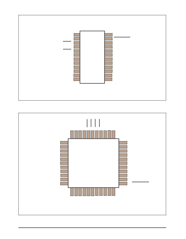
PINOUT (24-PIN SOIC & SSOP)
PINOUT (44-PIN QFP)
SP524
33
32
31
30
29
28
27
26
25
24
23
1
2
3
4
5
6
7
8
9
10
11
12
13
14
15
16
17
18
19
20
21
22
44
43
42
41
40
39
38
37
36
35
34
GND
VCC
R1INA
R1INB
R2INA
R2INB
R3INA
R3INB
R4INA
R4INB
T4OUTB
GND
T4OUT
A
VCC
T3OUTB
T3OUT
A
T2OUTB
T2OUT
A
VCC
T1OUTB
GND
T1OUT
A
ENT4
DP1
DP0
LATCH_EN
VSS
VDD
TIN4
TIN3
TIN2
TIN1
LOOPBCK
R1OUT
R2OUT
R3OUT
R4OUT
ENR1
ENR2
ENR3
ENR4
ENT1
ENT2
ENT3
R1OUT
LATCH_EN
ENR2
ENT2
ENR1
ENT1
DP1
DP0
T2IN
T1IN
T1OUTA
T1OUTB
SP522
R2OUT
LOOPBCK
VSS
VDD
R2INA
R2INB
R1INA
R1INB
T2OUTB
T2OUTA
GND
VCC
24
23
22
21
20
19
18
17
16
15
14
13
1
2
3
4
5
6
7
8
9
10
11
12

9
Rev. 7/10/03
SP522 Multi≠Mode Serial Transceivers
© Copyright 2003 Sipex Corporation
FEATURES
The SP522 and SP524 is a highly integrated
serial transceiver that offers programmability
between interface modes through software con-
trol. The SP522 and SP524 offers the hardware
interface modes for RS-232 (V.28), RS-422A
(V.11), RS-423 (V.10), and RS-485. The inter-
face mode selection is done via two control
pins. The SP522 contains two (2) independent
drivers and two (2) independent receivers. The
SP524 is basically two SP522 functions on one
silicon, thus having four (4) drivers and four (4)
receivers.
The SP522/SP524 is ideally suited for low-cost
wide area network connectivity and other multi-
protocol applications. Based on our previous
multi-mode SP500 family, Sipex has allocated
specific transceiver cells or "building blocks"
from the SP503 and created the SP522. The
"building block" concept is that these small
transceiver cells can be packaged to offer a
simple low-cost solution to networking appli-
cations that need only two to four interface
modes. The SP522 can be connected in series
to build multiple channels needed for the spe-
cific application. Sipex has conveniently
doubled the SP522 transceiver cell into the
SP524 on a single silicon. For example in a 8-
channel application requiring eight transceiv-
ers, the design can be implemented using two
SP524 devices. The SP522 and SP524 can also
be implemented in series with our SP500 fam-
ily. An application needing 9-channels can use
the SP504 containing seven (7) transceivers
with the SP522.
THEORY OF OPERATION
The SP522 and SP524 are simply made up of
the drivers, receivers, and decoder. The devices
operate on three (3) power supplies; V
CC
at
+5V, V
DD
at +10V , and V
SS
at ≠10V. Each of
these circuit blocks are described in more detail
below.
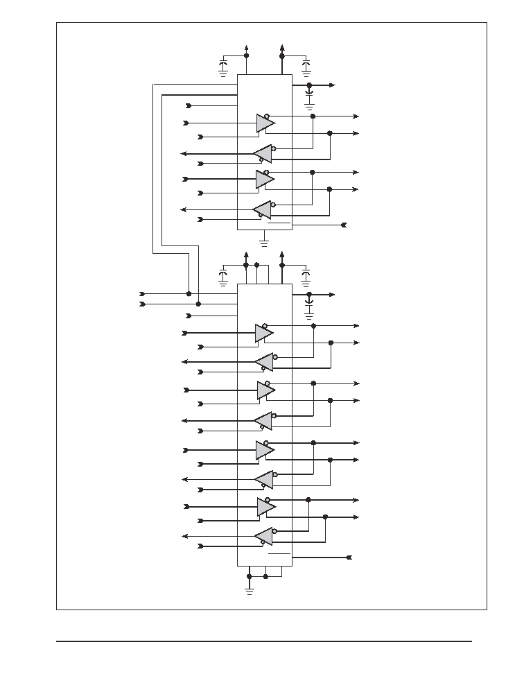
Drivers
The SP522 has two (2) enhanced independent
drivers. Control for the mode selection is done
via a two≠bit control word into DP0 and DP1.
The drivers are pre-arranged such that for each
mode of operation, the relative position and
functionality of the drivers are set up to accom-
modate the selected interface mode. As the
mode of the drivers is changed, the electrical
characteristics will change to support the
required signal levels. The mode of each driver
in the different interface modes that can be
selected is shown in Figures 10 to 13.
There are three basic types of driver circuits --
RS-232, RS-423, and RS-485.
The RS-232 drivers output single≠ended signals
with a minimum of +5V (with 3K
and 2500pF
loading), and can operate up to 120Kbps. The
RS-232 drivers are used in RS-232 mode for all
signals, and also in V.35 mode where they are
used as the control line signals such as DTR and
RTS.
The RS-423 drivers are also single≠ended
signals with a minimum voltage output of
+3.6V (with 450
loading) and can operate up
to 120Kbps. Open circuit V
OL
and V
OH
measurements are +4.0V to +6.0V when
supplying +5V to V
DD
and V
SS
. The RS-423
drivers can be used in RS-449, EIA-530, EIA-
530A and V.36 applications as Category II
signals from each of their corresponding
specifications.
The third type of driver produces a differential
signal that can maintain RS-485, +1.5V differ-
ential output levels with a worst case load of
54
. The signal levels and drive capability of
the RS-485 drivers allow the drivers to also
support RS-422 (V.11) requirements of +2V
differential output levels with 100
loads. The
RS-422 drivers can be used in RS-449,
EIA-530, EIA-530A and V.36 applications as
Category I signals which are used for clock and
data.
The drivers also have separate enable pins which
makes the SP522/SP524 helpful for half-duplex
applications. The enable pins will tri-state the
drivers when the ENT1 and ENT2 pins are at a
logic low ("0"). For the SP524, ENT3 and ENT4
are used for the two additional drivers. During
tri-stated conditions, the driver outputs will be
at a high impedance state.

10
Rev. 7/10/03
SP522 Multi≠Mode Serial Transceivers
© Copyright 2003 Sipex Corporation
Unused driver inputs can be left floating; pull≠
up resistors to +5V is internally connected on
the inputs so that the output is at a logic low
("0"). For differential drivers, the non-inverting
output will be at a logic high ("1").
Receivers
The SP522 has two (2) independent receivers
which can be programmed for the different
interface modes. Control for the mode selection
is done by DP0 and DP1.
Like the drivers, the receivers are pre-arranged
for the specific requirements of the interface. As
the operating mode of the receivers is changed,
the electrical characteristics will change to
support the required interface. Figures 10 to 13
show the mode of each receiver in the different
interface modes that can be selected.
There are three basic types of receiver circuits
-- RS-232, RS-423, and RS-485.
The RS-232 receiver is a single≠ended input
with a threshold of 0.8V to 3.0V. The RS-232
receiver has an operating voltage range of +15V
and can receive signals up to 120Kbps. The
input sensitivity complies with EIA-RS-232 and
V.28 at +3V to -3V. The input impedance is
3k
to 7k.
The RS-423 receivers are also single≠ended but
have an input threshold as low as +300mV. The
input impedance is guaranteed to be greater than
4K
, with an operating voltage range of +7V.
The RS-423 receivers can operate up to 120Kbps.
RS423 receivers can be used in RS-449, EIA530,
EIA-530A and V.36 applications as Category II
signals as indicated by their corresponding
specifications.
The third type of receiver is a differential which
supports RS-485. The RS-485 receiver has an
input impedance of 15K
and a differential
threshold of +300mV. Since the characteristics
of an RS-422 (V.11) receiver are actually
subsets of RS-485, the receivers for RS-422
requirements are covered by the RS-485 receivers.
RS-422 receivers are used in applications for
RS-449, EIA530, EIA-530A and V.36 as
Category I signals for receiving clock, data, and
some control line signals. The differential
receivers can receive data up to 10Mbps.
All receivers include a fail-safe feature that
output a known logic state when the receiver
inputs are unconnected. For single-ended
RS-232 receivers, there are internal 5k
pull-
down resistors on the inputs which produces a
logic high ("1") at the receiver outputs. The
single-ended RS-423 receivers produce a logic
low ("0") on the output when the inputs are
open. This is due to a pull-up device connected
to the input. The differential receivers have the
same internal pull-up device on the non-inverting
input which produces a logic high ("1") at the
receiver output.
The receivers also have enable pins which allow
for convenient half-duplex configurations. The
receivers are tri-stated when the ENR1 and
ENR2 pins are at a logic high ("1"). For the
SP524, ENR3 and ENR4 are used for the
additional two receivers.
In addition to the separate enable lines on each
transceiver, there is a latch enable pin,
LATCH_EN, which is used for enabling and
disabling the decoder control inputs (DP0, DP1)
and transceiver enable pins. This pin will
default to a logic high ("1") if not being used.
Loopback
The SP522 and SP524 contain a loopback fea-
ture that allows the driver outputs to "loopback"
to the receiver inputs for diagnostic testing in
the application. The loopback function is
activated when the LOOPBCK pin is low. When
in loopback mode, the driver outputs are
tri-stated and the receiver inputs are deactivated.
The receiver input impedance while in loopback
will be a minimum of 12k
. The loopback
function can be initiated during any mode of
operation, RS-232, RS-423 or RS-422. The
travel path of the transceivers in loopback is
shown on Figure 9. The loopback function
overrides the separate enable pins for the drivers
or receivers. When LOOPBCK is at a logic low
("0"), the device will be configured in loopback
regardless whether the transceiver is enabled or
disabled. If the loopback function is not
required, the LOOPBCK pin will default to a
logic high ("1") state.

11
Rev. 7/10/03
SP522 Multi≠Mode Serial Transceivers
© Copyright 2003 Sipex Corporation
Figure 9. Typical Operating Circuit, SP522 and SP524
T1IN
24
T1
T1OUTA
22
17
T2IN
25
T2
18
R1INA
44
R1OUT
43
R2OUT
T1OUTB
T2OUTA
T2OUTB
R1INB
R2INA
R2INB
LOOPBA
CK P
A
THS
V
DD
V
DD
10
µ
F
28
V
SS
10
µ
F
+5V
V
CC
10
µ
F
14
ENT1
ENT2
ENR1
ENR2
SP524
DP0
DP1
LATCH_EN
LOOPBCK
DECODER LOGIC
40
36
35
39
20
3
4
5
6
31
32
30
23
T3IN
26
T3
T3OUTA
16
11
T4IN
27
T4
13
R3INA
42
R3OUT
41
R4OUT
T3OUTB
T4OUTA
T4OUTB
R3INB
R4INA
R4INB
LOOPBA
CK P
A
THS
ENT3
ENT4
ENR3
ENR4
38
34
33
37
15
7
8
9
10
GND
12
1
21
2
19
V
SS
29
+
V
CC
V
CC
GND
GND
R2
R1
R3
R4
IN5819
T1IN
10
T1
T1OUTA
11
16
GND
14
T2IN
9
T2
15
R1INA
1
R1OUT
24
R2OUT
T1OUTB
T2OUTA
T2OUTB
R1INB
R2INA
R2INB
LOOPBA
CK P
A
THS
V
DD
V
DD
10
µ
F
21
V
SS
V
SS
10
µ
F
22
+5V
V
CC
10
µ
F
13
+
ENT1
ENT2
ENR1
ENR2
SP522
DP0
DP1
LATCH_EN
LOOPBCK
DECODER LOGIC
5
6
4
3
12
18
17
20
19
8
7
2
23
R1
R2
1N5819
12
Rev. 7/10/03
SP522 Multi≠Mode Serial Transceivers
© Copyright 2003 Sipex Corporation
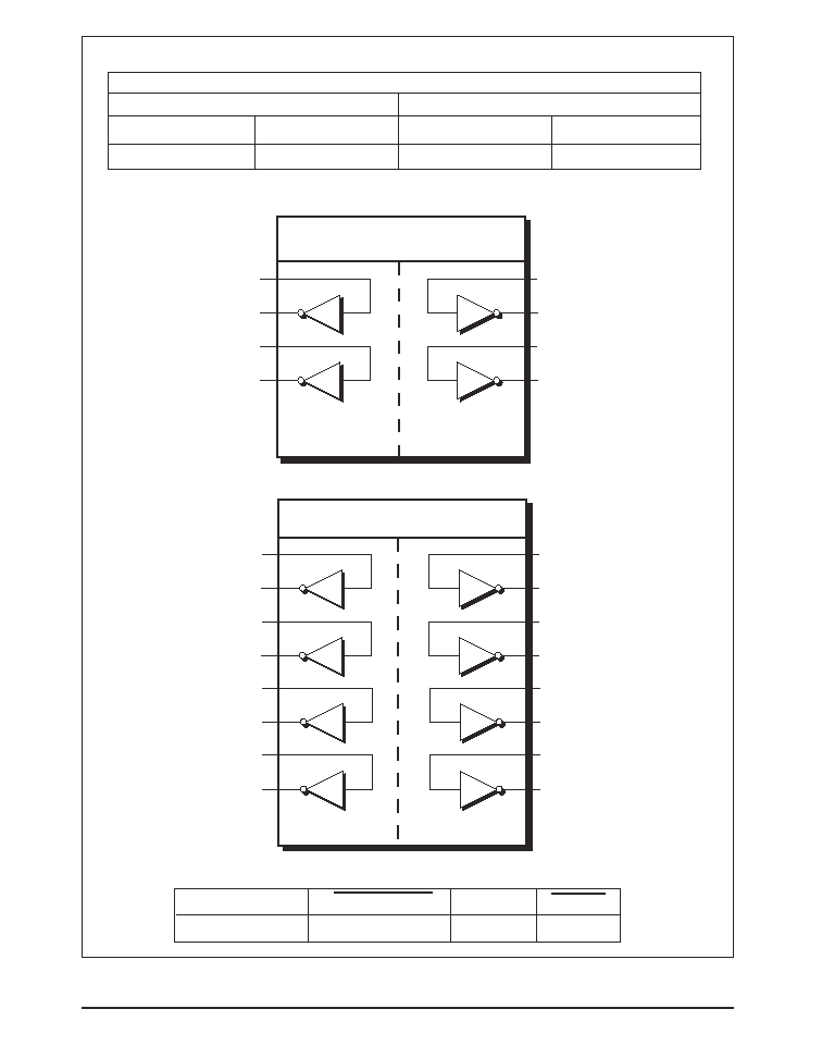
Figure 10. Mode Diagram -- RS232
MODE: RS232
DRIVER RECEIVER
DP0
DP1
DP0
DP1
R1INA (18)
1 0 1 0
LATCH_EN LOOPBCK
ENT
X
ENR
X
1
1
1
0
RECEIVERS DRIVERS
R2INA (20)
SP522
RECEIVERS DRIVERS
SP524
R2OUT (24)
R1OUT (1)
T1IN (10)
T1OUTA (11)
T2OUTA (15)
T2IN (9)
R1INA (3)
R2INA (5)
R2OUT (43)
R1OUT (44)
T1IN (24)
T1OUTA (22)
T2OUTA (18)
T2IN (25)
R3INA (7)
R4INA (9)
R4OUT (41)
R3OUT (42)
T3IN (26)
T3OUTA (16)
T4OUTA (13)
T4IN (27)

13
Rev. 7/10/03
SP522 Multi≠Mode Serial Transceivers
© Copyright 2003 Sipex Corporation
Figure 11. Mode Diagram -- RS423
MODE: RS423
DRIVER RECEIVER
DP0
DP1
DP0
DP1
R1INA (18)
1 1 1 1
LATCH_EN LOOPBCK
ENT
X
ENR
X
1
1
1
0
RECEIVERS DRIVERS
R2INA (20)
SP522
RECEIVERS DRIVERS
SP524
R2OUT (24)
R1OUT (1)
T1IN (10)
T1OUTA (11)
T2OUTA (15)
T2IN (9)
R1INA (3)
R2INA (5)
R2OUT (43)
R1OUT (44)
T1IN (24)
T1OUTA (22)
T2OUTA (18)
T2IN (25)
R3INA (7)
R4INA (9)
R4OUT (41)
R3OUT (42)
T3IN (26)
T3OUTA (16)
T4OUTA (13)
T4IN (27)

14
Rev. 7/10/03
SP522 Multi≠Mode Serial Transceivers
© Copyright 2003 Sipex Corporation
Figure 12. Mode Diagram -- RS422/RS485 for the SP522
MODE: RS422/485
DRIVER RECEIVER
DP0
DP1
DP0
DP1
0 1 0 1
LATCH_EN LOOPBCK
ENT
X
ENR
X
1
1
1
0
RECEIVERS DRIVERS
SP522
R1INA (18)
R1INB (17)
R1OUT (1)
T1IN (10)
T1OUTA (11)
T1OUTB (12)
R2INA (20)
R2INB (19)
R2OUT (24)
T2IN (9)
T2OUTA (15)
T2OUTB (16)

15
Rev. 7/10/03
SP522 Multi≠Mode Serial Transceivers
© Copyright 2003 Sipex Corporation
Figure 13. Mode Diagram -- RS422/RS485 for the SP524
MODE: RS422/485
DRIVER RECEIVER
DP0
DP1
DP0
DP1
0 1 0 1
LATCH_EN LOOPBCK
ENT
X
ENR
X
1
1
1
0
RECEIVERS DRIVERS
SP524
R1INA (3)
R1INB (4)
R1OUT (44)
T1IN (24)
T1OUTA (22)
T1OUTB (20)
R2INA (5)
R2INB (6)
R2OUT (43)
T2IN (25)
T2OUTA (18)
T2OUTB (17)
R3INA (7)
R3INB (8)
R3OUT (42)
T3IN (26)
T3OUTA (16)
T3OUTB (15)
R4INA (9)
R4INB (10)
R4OUT (41)
T4IN (27)
T4OUTA (13)
T4OUTB (11)

16
Rev. 7/10/03
SP522 Multi≠Mode Serial Transceivers
© Copyright 2003 Sipex Corporation
APPLICATIONS INFORMATION
DCE-DTE Applications
A serial port can be easily configured for DTE
and DCE using multiple SP522 and/or SP524
parts. As shown on Figure 14, the transceivers
are half-duplexed to provide convenient DCE-
DTE capability. The driver outputs are con-
nected to the receiver inputs with only one pair
out to the serial port for each driver/receiver.
When the driver is tri-stated by applying a logic
low ("0") to ENT, the receivers can be active to
receive the appropriate input. The driver output
during tri-state is high impedance, therefore
will not degrade the signal levels of the receiver
input signal. When the receiver is tri-stated by
applying a logic ("1") to ENR, the driver output
is active to drive the appropriate signal without
interference from the receiver. The receiver
inputs are at least 12k
to ground during tri-state.
Configuring Additional Multi-Protocol
Transceivers
Serial ports usually can have two data signals
(SD, RD), three clock signals (TT, ST, RT), and
at least eight control signals (CS, RS, etc.).
EIA-RS-449 contains twenty six signal types
including for a DB-37 connector. A DB-37
serial port design may require thirteen drivers
and fourteen receivers. Although many
applications do not use all these signals, some
applications may need to support extra
functions such as diagnostics. Sipex's SP504
supports enough transceivers for the primary
channels of data, clock and control signals.
Configuring LL, RL and TM may require two
additional drivers and one receiver if designing
for a DTE (one driver and two receivers for a
DCE).
The SP522 and SP524 is a convenient solution
in a design that requires two extra single ended
or differential transceivers. The SP504 and
SP522, shown in Figure 15, can be programmed
in various configurations. The SP504 is
programmed for RS-449 mode. By connecting
the decoder pins of the SP504 to the DP0 and
DP1 pins accordingly, the SP522 is programmed
in RS-423 mode. This adds two single ended
transceivers to the application. For applications
needing more than five RS-422 transceivers or
more than three RS-423 transceivers, the SP504
can be programmed to RS-422 whereas a SP524
can be added and programmed to RS-423, thus
creating seven RS-422 channels and four
RS-423 channels. The SP504 and the SP522/
SP524 can be configured to custom fit the
various serial port application needs.
+5V Only Operation Using the SP782
The SP522 and SP524 use external +10V or
+5V voltage supplies for power to maintain the
RS-232 and RS-423 voltage levels, respectively.
However, if a low-cost +5V solution if pre-
ferred, the SP522 and SP524 can be configured
with the SP782 or SP784 programmable charge
pump. The Sipex patent-pending programmable
charge pumps offer +10V or +5V outputs. The
programmability is used for switching from
RS-232 using the +10V outputs to RS-423 using
the +5V outputs. The SP782 requires 0.1
µF
capacitors and the SP784 requires 10
µF capacitors
for the charge pump. Please refer to the SP782
and SP784 data sheet for details on the program-
mable charge pump.
Achieving +10V with +12V Supplies
Since the SP522 and SP524 use external +10V
supplies, systems that have +12V supplies must
be regulated down to +10V. This can be simply
configured by placing diodes in series with the
V
DD
and V
SS
lines. The absolute maximum
supply voltage is +12V. Since most +12V power
supplies have some voltage tolerances, usually
+10%, any increase above the 12V maximum
will damage the device. However, the +12V
supply may be used providing that the maximum
supply voltages do not exceed the rated absolute
maximum V
SS
and V
DD
.
Sequencing of Power Supplies
Power Supplies for the SP522 and SP524 must
be sequenced. The recommended sequence is
V
CC
first, V
DD
50-80
µSec later and V
SS
100 to
1,000
µSec after V
DD
. There are no sequencing
requirements for the SP522 or SP524 when they
are powered from either the SP782 or SP784
charge pump devices or from the V
DD
and V
SS
supply pins of the SP504 or SP505 charge pump
powered devices. For further details, see the
application note, V
DD
, V
CC
and V
SS
Power
Supply Sequencing.
17
Rev. 7/10/03
SP522 Multi≠Mode Serial Transceivers
© Copyright 2003 Sipex Corporation
Figure 14. DTE/DCE Application with the SP522 and SP524
+5V
2
V
CC
SP524
43
28
29
10
µ
F
10
µ
F
22
20
24
25
5
36
DP1
DP0
+10V
10
µ
F
+
+
+
V
DD
V
SS
32
31
1
≠10V
39
40
LATCH_EN
30
LOOPBCK
GND
41
7
26
27
42
37
38
+5V
13
V
CC
SP522
1
15
21
22
10
µ
F
10
µ
F
11
12
10
9
18
24
DP1
DP0
+10V
10
µ
F
+
+
+
V
DD
V
SS
7
8
14
≠10V
6
17
5
3
LATCH_EN
2
LOOPBCK
GND
14 19
44
3
4
18
17
35
6
16
8
15
13
11
33
34
9
10
23
12
21
GND GND
16
6
20
19
4

18
Rev. 7/10/03
SP522 Multi≠Mode Serial Transceivers
© Copyright 2003 Sipex Corporation
Figure 15. Adding extra channels using the SP522 and SP504
CIRCUIT
CIRCUIT NAME
CIRCUIT
CIRCUIT
MNEMONIC
DIRECTION
TYPE
SG
SIGNAL GROUND
--------------
SC
SEND COMMON
TO DCE
RC
RECEIVE COMMON
FROM DCE
IS
TERMINAL IN SERVICE
TO DCE
IC
INCOMING CALL
FROM DCE
TR
TERMINAL READY
TO DCE
DM
DATA MODE
FROM DCE
SD
SEND DATA
TO DCE
RD
RECEIVE DATA
FROM DCE
TT
TERMINAL TIMING
TO DCE
ST
SEND TIMING
FROM DCE
RT
RECEIVE TIMING
FROM DCE
RS
REQUEST TO SEND
TO DCE
CS
CLEAR TO SEND
FROM DCE
RR
RECEIVER READY
FROM DCE
SQ
SIGNAL QUALITY
FROM DCE
NS
NEW SIGNAL
TO DCE
SF
SELECT FREQUENCY
TO DCE
SR
SIGNAL RATE SELECTOR
TO DCE
SI
SIGNAL RATE INDICATOR
FROM DCE
SSD
SECONDARY SEND DATA
TO DCE
SRD
SECONDARY RD
FROM DCE
SRS
SECONDARY RS
TO DCE
SCS
SECONDARY CS
FROM DCE
SRR
SECONDARY RR
FROM DCE
LL
LOCAL LOOPBACK
TO DCE
RL
REMOTE LOOPBACK
TO DCE
TM
TEST MODE
FROM DCE
SS
SELECT STANDBY
TO DCE
SB
STANDBY INDICATOR
FROM DCE
RS-449 Interchange Circuits Table
CONTROL
COMMON
DATA
TIMING
CONTROL
DATA
CONTROL
CONTROL
CONTROL
PRIMARY CHANNEL
SECONDARY
CHANNEL
V
CC
V
DD
61
59
+5V
SP504CF
Drivers
TxD
14
58
56
DTR
13
54
52
RTS
16
63
65
TxC
15
42
44
ST
22
47
45
RL
17
51
49
LL
24
70
71
RxD
1
37
38
RxC
20
66
67
CTS
80
68
69
DSR
78
35
36
DCD
19
39
40
RI
21
76
77
SCT
79
Receivers
see pinout diagram for various ground pins
4
22
12
30
7
25
17
35
6
24
8
26
9
27
11
29
13
31
15
5
23
DB-37 Connector
10
14
32
V
SS
22
µ
F
22
µ
F
22
µ
F
22
µ
F
various VCC
supply pins
27
26
30
28
31
1N5819
C1-
C2-
C1+
C2+
10
µ
F
12
11
10
9
TDEC0
TDEC1
TDEC2
TDEC3
RDEC0
RDEC1
RDEC2
RDEC3
2
3
4
5
+5V
13
V
CC
SP522
1
20
21
22
10
µ
F
10
µ
F
11
15
10
9
18
24
1
0
0
1
Tied to
TDEC0
Tied to
TDEC1
DP1
DP0
+5V
10
µ
F
+
+
+
+
+
+
+
+
V
DD
V
SS
7
8
14
RS-449 Mode
RS-423 Outputs
RS-423 Inputs
≠5V
6
4
5
3
LATCH_EN
2
LOOPBCK
GND

19
Rev. 7/10/03
SP522 Multi≠Mode Serial Transceivers
© Copyright 2003 Sipex Corporation
D
E
H
PACKAGE: PLASTIC
SMALL OUTLINE (SOIC)
(WIDE)
DIMENSIONS (Inches)
Minimum/Maximum
(mm)
A
A1
ÿ
L
B
e
A
A1
B
D
E
e
H
L
ÿ
24≠PIN
0.093/0.104
(2.352/2.649)
0.004/0.012
(0.102/0.300)
0.013/0.020
(0.330/0.508)
0.599/0.614
(15.20/15.59)
0.291/0.299
(7.402/7.600)
0.050 BSC
(1.270 BSC)
0.394/0.419
(10.00/10.64)
0.016/0.050
(0.406/1.270)
0∞/8∞
(0∞/8∞)

20
Rev. 7/10/03
SP522 Multi≠Mode Serial Transceivers
© Copyright 2003 Sipex Corporation
D
E
H
PACKAGE: PLASTIC
SHRINK
SMALL OUTLINE
(SSOP)
DIMENSIONS (Inches)
Minimum/Maximum
(mm)
24≠PIN
A
A1
ÿ
L
B
e
A
A1
B
D
E
e
H
L
ÿ
0.068/0.078
(1.73/1.99)
0.002/0.008
(0.05/0.21)
0.010/0.015
(0.25/0.38)
0.317/0.328
(8.07/8.33)
0.205/0.212
(5.20/5.38)
0.0256 BSC
(0.65 BSC)
0.301/0.311
(7.65/7.90)
0.022/0.037
(0.55/0.95)
0∞/8∞
(0∞/8∞)

21
Rev. 7/10/03
SP522 Multi≠Mode Serial Transceivers
© Copyright 2003 Sipex Corporation
44 PIN MQFP (MS-022 BC)
L1
5
∞
-16
∞
0
∞
MIN.
0
∞
≠7
∞
5
∞
-16
∞
L
0.30" RAD. TYP.
0.20" RAD. TYP.
c
E1
1
D1
D
CL
CL
-B-
-D-
-A-
1
E
e
Seating
Plane
A1
A
A
b
A2
D2
E2
1
DIMENSIONS
Minimum/Maximum
(mm)
SYMBOL
A
A1
A2
b
D
D1
D2
E
E1
E2
e
N
44≠PIN MQFP
JEDEC MS-022
(AB) Variation
MIN
NOM
MAX
2.45
0.00
0.25
1.80
2.00
2.20
0.29
0.45
13.20 BSC
10.00 BSC
8.00 REF
13.20 BSC
10.00 BSC
8.00 REF
0.80 BSC
44
COMMON DIMENTIONS
SYMBL MIN
NOM
MAX
c
0.11
23.00
L
0.73
0.88
1.03
L1
1.60 BASIC
PACKAGE: 44 Pin MQFP

22
Rev. 7/10/03
SP522 Multi≠Mode Serial Transceivers
© Copyright 2003 Sipex Corporation
44 PIN LQFP
L
11
∞
- 13
∞
0
∞
Min
11
∞
- 13
∞
0
∞
≠7
∞
DIMENSIONS
Minimum/Maximum
(mm)
SYMBOL
A
A1
A2
b
D
D1
e
E
E1
N
44≠PIN LQFP
JEDEC MS-026
(BCB) Variation
MIN
NOM
MAX
1.60
0.05
0.15
1.35
1.40
1.45
0.30
0.37
0.50
12.00 BSC
10.00 BSC
0.80 BSC
12.00 BSC
10.00 BSC
44
c
L1
b
e
A2
COMMON DIMENTIONS
SYMBL MIN
NOM
MAX
c
0.11
23.00
L
0.45
0.60
0.75
L1
1.00 BASIC
0.2 RAD. MAX.
0.08 RAD. MIN.
Seating
Plane
A1
A
A
E
1
D
1
D
CL
CL
-D-
Pin 1
E
PACKAGE: 44 Pin LQFP

23
Rev. 7/10/03
SP522 Multi≠Mode Serial Transceivers
© Copyright 2003 Sipex Corporation
ORDERING INFORMATION
Model
Temperature Range
Package Types
SP522CT ........................................................................... 0
∞
C to +70
∞
C .............................................................................................. 24-pin SOIC
SP522CA .......................................................................... 0
∞
C to +70
∞
C ............................................................................................. 24-pin SSOP
SP524CF ........................................................................... 0
∞
C to +70
∞
C ............................................................................................ 44-pin MQFP
Sipex Corporation reserves the right to make changes to any products described herein. Sipex does not assume any liability arising out of the
application or use of any product or circuit described hereing; neither does it convey any license under its patent rights nor the rights of others.
Corporation
ANALOG EXCELLENCE
Sipex Corporation
Headquarters and
Sales Office
233 South Hillview Drive
Milpitas, CA 95035
TEL: (408) 934-7500
FAX: (408) 935-7600
Sales Office
22 Linnell Circle
Billerica, MA 01821
TEL: (978) 667-8700
FAX: (978) 670-9001
e-mail: sales@sipex.com
Please consult the factory for pricing and availability on a Tape-On-Reel option.