 | –≠–ª–µ–∫—Ç—Ä–æ–Ω–Ω—ã–π –∫–æ–º–ø–æ–Ω–µ–Ω—Ç: SP6122 | –°–∫–∞—á–∞—Ç—å:  PDF PDF  ZIP ZIP |

1
Rev. 7/16/03
SP6122 Low Voltage, Micro 8, PFET, Buck Controller © Copyright 2003 Sipex Corporation
SP6122
Optimized for Single Supply, 3V - 5.5V Applications
High Efficiency, Greater than 90% Possible
Small Micro 8 Package
20ns/1nF PFET Output Driver
Fast Transient Response
Open Drain Fault Output Pin
Internal Soft Start Circuit
Accurate 1.5% Reference
Programmable Output Voltage or Fixed 1.5V Output
Loss-less Adjustable Current Limit with High side
R
DS(ON)
Sensing
Hiccup or Lock-up Fault Modes
Low 5
µ
A Sleep Mode Quiescent Current
Low 300
µ
A Protected Mode Quiescent Current
Ultra Low, 150
µ
A Unprotected Mode Quiescent
Current
High Light Load Efficiency
Low Voltage, Micro 8, PFET, Buck Controller
Ideal for 1A to 5A, Small Footprint, DC-DC Power Converters
APPLICATIONS
Video Cards
High Power Portable
Microcontrollers
I/O & Logic
Industrial Control
Distributed Power
Low Voltage Power
DESCRIPTION
The SP6122 is a PFM minimum on-time controller designed to work from a single 5V or 3.3V
input supply. It is engineered specifically for size and minimum components count, simplifying
the transition from a linear regulator to a switcher solution. However, unlike other "micro"
parts, the SP6122 has an array of value added features like optional hiccup mode, over
current protection, TTL enable, "jitter and frequency stabilization" and a fault flag pull down
pin. Combined with reference and driver specifications usually found on more expensive
integrated circuits, the SP6122 delivers great performance and value in a micro 8 package.
Æ
1
2
3
4
5
6
7
8
ENABLE
V
OUT
FFLAG
PDRV
GND
I
SET
I
SENSE
V
CC
SP6122
8 Pin
µ
SOIC
SP6122
V
CC
FFLAG
V
OUT
ENABLE
PDRV
GND
I
SET
I
SENSE
FFLAG
V
OUT
R
SET
1k
DFLY
Q1
PDS6375
ENABLE
C1
4.7
µ
F
V
IN
3.0V to 7.0V
L1
2.2
µ
H
C
OUT
470
µ
F
1A to 5A
Æ
Æ
R1
5
C2
100
µ
F
STPS2L25U
FEATURES
TYPICAL APPLICATION CIRCUIT

2
Rev. 7/16/03
SP6122 Low Voltage, Micro 8, PFET, Buck Controller © Copyright 2003 Sipex Corporation
ELECTRICAL CHARACTERISTICS
Unless otherwise specified: 0∞C < T
AMB
< 70∞C, 3.0V < V
CC
< 5.5V, C
PDRV
= 1nF, V
ENABLE
= V
CC
, V
FFLAG
= V
CC
,
I
SET
= I
SENSE
= V
CC
, GND = 0V
These are stress ratings only and functional operation of
the device at these ratings or any other above those
indicated in the operation sections of the specifications
below is not implied. Exposure to absolute maximum
rating conditions for extended periods of time may affect
reliability.
V
CC ..............................................................................................................
7V
All other pins ...................................... -0.3V to V
CC
+0.3V
Peak Output Current < 10
µ
s
PDRV ......................................................................... 2A
Storage Temperature .............................. -65
∞
C to 150
∞
C
Power Dissipation
Lead Temperature (Soldering, 10 sec) ................. 300
∞
C
ESD Rating ...................................................... 2kV HBM
PARAMETER
MIN
TYP
MAX
UNITS
CONDITIONS
QUIESCENT CURRENT
V
CC
Supply Current,
OVC Enabled
-
300
450
µ
A
No Switching, I
SET
= I
SENSE
= V
CC
V
CC
Supply Current,
OVC Disabled
-
250
360
µ
A
No Switching, I
SET
= I
SENSE
= 0
V
CC
Supply Current,
-
150
225
µ
A
No Switching, ISET
= 0,
OVC Disabled, Ultra Low IQ
I
SENSE
=V
CC
V
CC
Supply Current, Sleep Mode
-
5
15
µ
A
Enable=0
REFERENCE
Output Voltage, Initial Accuracy
VR*0.985
VR
VR*1.015
V
VR = Factory Set Voltage,
see Note
Output Voltage, Over Line,
VR*0.980
VR
VR*1.020
V
VR = Factory Set Voltage,
Load and Temperature
see Note
Reference Comparator
-
5
-
mV
Internal Hysteresis at Feedback
Hysteresis
Terminal
V
OUT
Input Current
-
23
-
µ
A
V
OUT
= VR;
SP6122ACU-1.5 ONLY
OSCILLATOR
Oscillator Frequency
210
300
390
kHz
Minimum Pulse Width during
150
270
380
ns
Startup (Blanking Time)
Soft Start
Soft Start Ramp Time
-
3.5
-
ms
V
OUT
= VR ≠ 30mV, Measure
time from ENABLE = 1V to
PDRV Low
Soft Start Voltage when
-
250
-
mV
Measure VSoft Start when
PDRV Switches
PDRV goes Low. (internal)
ABSOLUTE MAXIMUM RATINGS

3
Rev. 7/16/03
SP6122 Low Voltage, Micro 8, PFET, Buck Controller © Copyright 2003 Sipex Corporation
PARAMETER
MIN
TYP
MAX
UNITS
CONDITIONS
RDS OVER CURRENT COMPARATOR
Over Current Comparator
130
150
180
mV
V(I
SET
) - V(I
SENSE
) 25
∞
C only
Threshold Voltage
Threshold Voltage Temperature
-
3800
-
ppm/
∞
C
Coefficient
I
SET
Sink Current
15
20
25
µ
A
Current into I
SET
25
∞
C only
I
SET
Current Temperature
-
4300
-
ppm/
∞
C
Coefficient
I
SENSE
Input Bias Current
-
-
100
nA
I
SET
, I
SENSE
Common Mode
2.0
-
V
CC
V
Input Range
Over Current Peak Detection
-
10
-
µ
s
Time Constant
ENABLE INPUT & FFLAG OUTPUT
ENABLE Threshold
0.90
1.21
1.45
V
ENABLE Pin Source Current
0.8
5.0
10.0
µ
A
FFLAG Sink Current
3.0
7.5
15.0
mA
V(FFLAG) = 1V
GATE DRIVER
PDRV Rise Time
20
75
ns
0.5V to 4.5V
PDRV Fall Time
20
75
ns
4.5V to 0.5V
NOTE: Available Output Voltages: 1.5V Fixed, 1.25V Adj.
ELECTRICAL CHARACTERISTICS: Continued
Unless otherwise specified: 0∞C < T
AMB
< 70∞C, 3.0V < V
CC
< 5.5V, C
PDRV
= 1nF, V
ENABLE
= V
CC
, V
FFLAG
= V
CC
,
I
SET
= I
SENSE
= V
CC
, GND = 0V

4
Rev. 7/16/03
SP6122 Low Voltage, Micro 8, PFET, Buck Controller © Copyright 2003 Sipex Corporation
PIN DESCRIPTION
PIN #
PIN NAME
DESCRIPTION
1
V
CC
Main Supply Pin: A RC filter as shown in the application circuit is
recommended. The decoupling capacitor needs to be close to the pin.
2
FFLAG
Fault Flag Pull-down Pin: Sinks current during a fault condition. Can
be hooked up to ENABLE to initiate Hiccup Timing.
3
V
OUT
Regulated Output Voltage: This voltage is divided internally and
compared to a 1.5%, 1.25V reference at the PFM comparator.
4
ENABLE
Enable Input: Floating this pin or pulling above 1.45V enables the
part. Pulling this pin to less than 0.9V will disable the part. A minimum
100pF capacitor is required between this pin and Ground to ensure
proper startup. If FFLAG is hooked to ENABLE, the capacitor on
ENABLE will control hiccup timing.
5
I
SENSE
Negative Input to the Over Current Amplifier/Comparator: This input
is subtracted from the I
SET
input and gained by a factor of 3.3. The
output of this amplifier is compared with a 0.5V threshold, yielding a
150mV threshold. This threshold has a 3800 ppm/
∞
C temperature
coefficient. If the subtraction exceeds 150mV, charge is pumped into
a capacitor until the capacitor hits V
CC
/2. At this time, the over current
fault is activated. If I
SET
= 0V and I
SENSE
= V
CC
, the part enters an
unprotected, 150
µ
A quiescent current mode.
6
I
SET
Positive Input to the Over Current Amplifier: 20
µ
A flows into the I
SET
pin if it is pulled through a resistor to V
IN
. This current has a
4300ppm/
∞
C temperature coefficient and can be used via external
resistor to raise the overcurrent trip point from 150mV to some higher
value. If I
SET
= 0V and I
SENSE
= 0V, the part enters an unprotected,
250
µ
A quiescent current mode.
7
GND
Power and Analog Ground: Hook directly to output ground.
8
PDRV
Drive for PFET High Side Switch: 1nF/20ns Output Driver.

5
Rev. 7/16/03
SP6122 Low Voltage, Micro 8, PFET, Buck Controller © Copyright 2003 Sipex Corporation
BLOCK DIAGRAM
+
-
-
+
-
+
-
+
PFET
Driver
Driver
Logic
S
Q
R
Reset
Dominant
S
Q
R
200ns Blanking
One Shot
ENABLE
I
SET
V
OUT
I
SENSE
Reference
5
4
3
6
SS
1.25V
Reference
Comparator
1V
FFLAG
2
7
GND
8
1
PFET OFF
RESET
Dominant
PFET OFF
FAULT
+
-
X 3.3
500mV
(3800 ppm/
∞
C)
PDRV
T
ON
Min On Time Clock
PDRV
V
CC
Loop
Latch
QB
V
OUT
* K1
Soft Start Clock
S
Q
R
Run
Latch
QB
S
R
SS
Latch
QB
Reset
Dominant
Start On Time
Soft Start
Reset
Dominant
POR
X K1
Over Current
(Gated S&H)
POR
I
SET
< 1V
Low IQ
I
SET
I
SENSE
POR
Blank
20
µ
A
(4300 ppm/
∞
C)

6
Rev. 7/16/03
SP6122 Low Voltage, Micro 8, PFET, Buck Controller © Copyright 2003 Sipex Corporation
General Overview
The SP6122 is a minimum on-time, PFM
controller for low cost DC/DC step down
converters. The main control loop consists
of a REFERENCE COMPARATOR, an ON-
TIME CLOCK, a LOOP LATCH and a
BLANKING ONESHOT. The REFERENCE
comparator has 10mV of internal hysteresis
and a 1.25V internal reference. Both hyster-
esis and reference voltage are multiplied
upward by the internal feedback resistor
divider, K1 (K1 = 1 for the adjustable ver-
sion). This value is set by the factory and
determines the output voltage of the con-
verter. This divider is also used in the on-
time algorithm for the controller. If the out-
put voltage drops below K1*1.25V, then the
DRIVER LOGIC tells the PFET switch to be
"on" for a certain minimum time. The on-
time is set by the Soft Start CLOCK fre-
quency and is factory programmed to run at
300kHz. When the part is enabled, through
V
CC
or the ENABLE pin, the DRIVER LOGIC
is configured to first look at the fixed fre-
quency Soft Start loop. The output voltage
is then controlled by a 0.5V/ms internal
ramp. When the output voltage reaches
K1*1.25V, the Soft Start loop is switched off
and the main loop takes over.
Fault management is controlled either
through power-on-reset (POR) or R
DS(ON)
sense over current protection. Should an
over current condition occur, the SP6122
will completely "lock-up" and turn the PFET
switch off. The only way to recover will be to
either cycle the ENABLE pin or V
CC
. A Fault
flag output (FFLAG) has been included to
either signal the upstream circuitry or to
engage a hiccup mode that will restart the
SP6122. Tying FFLAG to ENABLE allows
the controller to restart without assistance.
Lastly, the SP6122 includes a powerful 4
PFET driver stage designed to drive a PFET
associated with high speed converter de-
signs in the 1 A ≠ 5 A range.
Enable
Low quiescent mode or "Sleep Mode" is
initiated by pulling the ENABLE pin below
650mV. The ENABLE pin has an internal
4
µ
A pull-up current and does not require
any external interface for normal operation.
If the ENABLE pin is driven from a voltage
source, the voltage must be above 1.45V in
order to guarantee proper "awake" opera-
tion. Assuming that V
CC
is above about
2.9V, the SP6122 transitions from "Sleep
Mode" to "Awake Mode" in about 20
µ
s ≠
30
µ
s and from "Awake Mode" to "Sleep
Mode" in a few microseconds. SP6122 qui-
escent current in sleep mode is 5
µ
A typical.
During Sleep Mode, the PFET switch is
turned off, the internal SS voltage is held
low and the FFLAG pin is high impedance.
Low Current Operation
If over current fault protection is not needed,
the SP6122 offers two options to lower its
quiescent current. By grounding both I
SET
and I
SENSE
pins, the circuitry responsible for
over current detection is turned off. This
option results in a saving of about 50
µ
A in
quiescent current. Option two requires that
I
SET
is grounded and ISENSE is greater
than 1.3V. This option put the SP6122 in a
low performance mode that cuts the operat-
ing frequency roughly in half and slows
down critical comparators in the main loop.
Option two can result in additional saving of
100
µ
A bringing the total quiescent current
to only 150
µ
A (typ).
Power On Reset (POR)
The POR command is given every time the
bandgap reference is started. The internal
1.25 V reference is compared against a 1V
NFET threshold. When the reference is below
the threshold, FAULT and RUN latches are
reset, the internal SS voltage is discharged
and the PFET switch is "off". The SP6122 is
allowed to begin a soft start cycle when the
THEORY OF OPERATION
7
Rev. 7/16/03
SP6122 Low Voltage, Micro 8, PFET, Buck Controller © Copyright 2003 Sipex Corporation
Power On Reset (POR): continued
internal 1.25V is greater than the 1 V thresh-
old. Note this is a "loose" threshold and should
not be used to guarantee under voltage lock
out with respect to V
CC
. Care should be take
to ensure that V
CC
does not "get stuck" on the
way to its regulated value.
Soft Start
Soft start is required on step-down control-
lers to prevent excess inrush current through
the power train during start-up. On the
SP6122, this is managed through turning
the PFET switch on with a fixed frequency
clock and then turning the switch off when
divided down version of the output voltage
exceeds the internal SS voltage ramp. The
internal SS voltage ramp rises with a 0.5 V/
ms slew rate and the internal feedback
voltage follows this rate of change. The
presence of the output capacitor creates
extra current draw during startup. Since
dV
OUT
/dt creates an average sustained cur-
rent in the output capacitor, this current
must be considered while calculating peak
inrush current and over current thresholds.
An expression to determine the excess in-
rush current due to the dV
OUT
/dt of the
output capacitor is:
IC
OUT
= C
OUT
*0.5 V/ms *
V
OUT
,
V
R
where VR is the internal reference voltage.
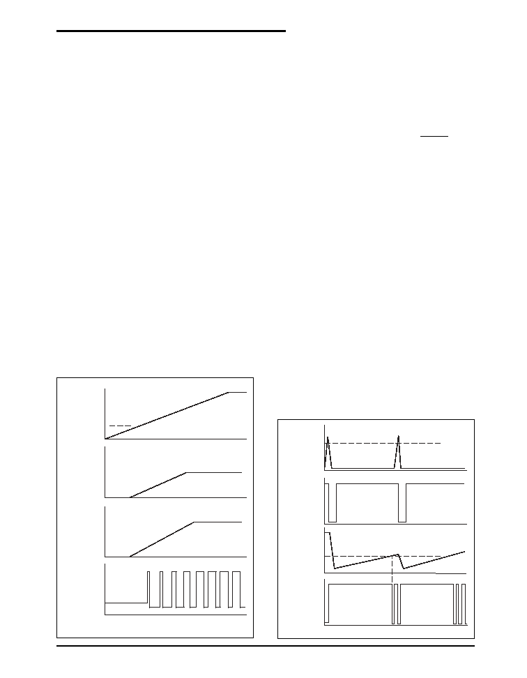
Lock Up & Hiccup Modes
As previously stated, if the SP6122 detects
an over current condition and initiates a
fault, the power supply remains "locked up".
That is, the FFLAG pin immediately pulls
low (if loaded) and the PFET switch turns
off. This condition is permanent unless the
either the V
CC
or ENABLE is cycled. How-
ever if FFLAG is tied to ENABLE, the SP6122
will restart without assistance (Hiccup
Mode). Furthermore, the restart time can be
controlled by the addition of a small capaci-
tor on the ENABLE pin to ground. The
restart time is equal to the amount of time it
takes for the 5
µ
A ENABLE pin current to
charge the external capacitor to an NFET
threshold (roughly 1V). The waveforms that
describe the Hiccup Mode operation are
shown below.
TIME
SWN
Voltage
V(V
IN
)
0V
Inductor
Current
I
LOAD
0A
Comparator
Reference
Voltage
1.25V
0V
0V
0.25V
SS
Voltage
dV
SS
/dt = 0.5Vms
VI
SET
- VI
SENSE
0V
1.0V
V(V
CC
)
0V
0V
0V
FFLAG
Voltage
ENABLE
Voltage
150mV
TIME
dV
ENABLE
/dt = 4
µ
A/C
ENABLE
PDRV
Voltage
V(V
CC
)
V(V
CC
)
THEORY OF OPERATION: Continued

8
Rev. 7/16/03
SP6122 Low Voltage, Micro 8, PFET, Buck Controller © Copyright 2003 Sipex Corporation
V(V
CC)
TIME
PDRV
Voltage
- V(V
DIODE
)
0V
SWN
Voltage
V(V
CC)
= V
IN
0 V
Gate Driver Test Conditions
10 %
90 %
5 V
FALL TIME
RISE TIME
10 %
90 %
PDRV
Over Current Protection
Over current protection on the SP6122 is
implemented through detection of an ex-
cess voltage condition across the PFET
switch during conduction. This is typically
referred to as high side R
DS(ON)
detection.
The over current comparator charges a
sampling capacitor each time V(I
SET
) ≠
V(I
SENSE
) exceeds 150mV (typ) and the
PDRV voltage is low. The discharge cur-
rent/charge current ratio on the sampling
capacitor is about 2%. Therefore, provided
that the over current condition persists, the
capacitor voltage will be pumped up during
each time PDRV switches low and this
voltage will trigger an over current condition
upon reaching a CMOS inverter threshold.
There are many advantages to this ap-
proach. First, the filtering action of the gated
S/H scheme protects against false trigger-
ing during a transient load condition or sup-
ply line noise. In addition, the total amount
of time to trigger the fault depends on the
on-time of the PFET switch. Ten, 1
µ
s pulses
are equivalent to twenty, 500ns pulses or
one, 1
µ
s pulse, however, depending on the
period, each scenario takes a different
amount of total time to trigger a fault. There-
fore, the fault becomes an indicator of aver-
age power in the PFET switch. Also, be-
cause the CMOS trip threshold is depen-
dent on V
CC
, the over current scheme is
protected against false triggering due to
changes in line voltage.
Although the 150mV threshold is fixed, the
overall R
DS(ON)
detection voltage can be
increased by placing a resistor from I
SET
to
V
CC
. A 20
µ
A sink current programs the
additional voltage.
The 150 mV threshold and 20
µ
A I
SET
cur-
rent have 3800 ppm/
∞
C and 4300 ppm/
∞
C
temperature coefficients, respectively.
These TC's are designed into the SP6122
in an effort to match the thermal character-
istics of the PFET switch. It assumed that
the SP6122 will be used in compact designs
where there is a high amount of thermal
coupling between the PFET and the con-
troller.
Light Load Operation
One of the advantages of the SP6122 mini-
mum on-time control scheme is the loop's
ability to seamlessly and efficiently transi-
tion from heavy loads to light loads. In most
other control schemes, the controller is no-
tified about a light load condition and then
must abruptly change control schemes in
order to maintain efficiency. The SP6122
simply reduces the frequency when the
average load current is less than the aver-
age inductor ripple current. As a result,
switching loss decreases as the load cur-
rent decreases and overall efficiency is
maintained.
Output Driver
The driver stage consists of a high side, 4
ohm PFET driver. The following waveforms
illustrate basic behavior of the driver.
THEORY OF OPERATION: Continued

9
Rev. 7/16/03
SP6122 Low Voltage, Micro 8, PFET, Buck Controller © Copyright 2003 Sipex Corporation
SP6122
V
CC
FFLAG
V
OUT
ENABLE
PDRV
GND
I
SET
I
SENSE
FFLAG
V
OUT
RS
1.00k
DS
STPS2L25U
Q1
ENABLE
C
IN
47
µ
F
Ceramic
V
IN
+3.3V
2.2
µ
H
+1.9V
Æ
Æ
1
2
3
J1
CEN
4.7nF
GND
L1
C
OUT
470
µ
F
+
R1
6.5k
R2
12.5k
+ C1
4.7
µ
F
Ceramic
1
2
3
4
8
7
6
5
V
OUT
PMOS
PDS6375
Figure 1. SP6122 Evaluation Board Application Schematic
As an SP6122 application example, we will
use the circuit from the SP6122 Evaluation
Board Manual. This evaluation board uses
the Sipex SP6122ACU, 1.25V adjustable
PFET controller to realize a 3.3V to 1.9V
step down converter. The board is opti-
mized for 1A ≠ 4A operation and has an
R
DS(ON)
over current trip threshold of about
7A. The body of the applications section
contains:
∑ Data for the Evaluation Board
∑ Guidelines for Component Selection
∑ Features and Protection
∑ Layout Guidelines
∑ Introduction to the "Buck Cad Calculator"
Spreadsheet
Data For Evaluation Board
The SP6122 is engineered for size and mini-
mum pin count, yet has a very accurate 2.0%
reference over line, load and temperature.
Figure 2 data shows a typical SP6122 Evalu-
ation Board Efficiency plot, with efficiencies to
88% and output currents to 4A. Load Regula-
tion plot in Figure 3 shows an essentially flat
response of only 3mV change for up to 4A
load. Figure 4 Line Regulation illustrates a
1.90V output that varies only 4mV or 0.2% for
an input voltage change from 3.0V to 5.5V.
While data on individual power supply boards
may vary, the capability of the SP6122 of
achieving high accuracy over load and line
shown here is quite impressive and desirable
for accurate power supply design.
83
84
85
86
87
88
89
0
1
2
3
4
5
I
LOAD
(A)
Efficiency (%)
Figure 2. SP6122 Efficiency with V
IN
= 3.3V,
V
OUT
= 1.9V.
APPLICATION INFORMATION

10
Rev. 7/16/03
SP6122 Low Voltage, Micro 8, PFET, Buck Controller © Copyright 2003 Sipex Corporation
Guidelines for Component Selection
GENERAL
The SP6122 is a minimum on-time PFM
controller. This means there is no error amp
controlling the loop. Although an internal
algorithm adjusts the on-time approximate
the performance of a fixed frequency con-
troller, the loop control is generated by
looking at OUTPUT RIPPLE. The peak to
peak value of this output ripple must be no
less than 2% of the DC output voltage in
order to maintain reasonable fixed frequency
operation. In addition, as with all PFM con-
trollers, board layout is critical and careful
attention must be paid to minimize paths
that can generate noise. Fortunately, the
SP6122 is designed for simplicity and minimal
external components, making it easy to de-
sign small, quiet power converters up to 12W.
INDUCTOR SELECTION
In a SP6122 application, the main factors
for choosing an inductor are likely to be
cost, size, saturation current and efficiency.
If you use low inductor values, you get the
smallest size, but you may cause larger
ripple currents and poor efficiency and re-
quire more output capacitance to smooth
the output ripple. Increasing the inductor
value will decrease the output voltage ripple
but degrade the transient response. For a
good compromise between size, losses and
cost, set the inductor ripple current between
20% to 40% of the maximum output current.
The inductor operating point and switching
frequency determine the inductor value as
seen in the following expression:
L = (V
OUT
+ V
DIODE
)*(V
IN
≠ V
OUT
)/
((V
IN
+ V
DIODE
)*(
F
S
K
R
I
OUT(max)
))
Where F
S
= switching frequency (see Soft
Start Frequency Specification)
K
R
= ratio of the ac inductor ripple current to
the maximum output current
V
DIODE =
forward Schottky diode voltage
For an application with 1.9V out, 4A maxi-
mum I
OUT
, 3.3V input supply, 400 mV typical
forward diode voltage, 300kHz frequency
and a 30% inductor ripple current, a 2.2
µ
H
inductor was selected (see Table 1 SP6122
Component Selection).
The peak to peak inductor ripple current is:
I
PP
= (V
OUT
+ V
DIODE
)*(V
IN
≠ V
OUT
)/
((V
IN
+ V
DIODE
)*(
F
S
L))
For that same 2.2
µ
H inductor application,
the I
PP
= 1.32A.
The inductor must be selected to not satu-
rate the core at the peak inductor current:
I
PEAK
= I
OUT(max)
+ I
PP
/2
Figure 3. SP6122 Load Regulation with Input
Voltage = 3.3V.
Figure 4. SP6122 Line Regulation with I
LOAD
= 2A.
1.897
1.898
1.899
1.900
1.901
1.902
0
1
2
3
4
5
V
OUT
(V)
I
LOAD
(A)
1.899
1.900
1.901
1.902
1.903
1.904
1.905
3
4
5
6
V
OUT
(V)
I
LOAD
(A)
APPLICATION INFORMATION: Continued

11
Rev. 7/16/03
SP6122 Low Voltage, Micro 8, PFET, Buck Controller © Copyright 2003 Sipex Corporation
Again, for that same 2.2
µ
H application, I
PEAK
= 4.6A. Therefore, a 2.2
µ
H inductor with at
least a 5A rating would be desired.
The type of core material to use must also
be determined. For low cost, powdered iron
cores can be used, and they have a gradual
saturation characteristic, but they can cause
ac core loss when the inductor value is low
and ripple current is high. Ferrite cores, on
the other hand, have an abrupt saturation
characteristic and the inductor value drops
sharply when the peak design current is
exceeded. But, ferrites are preferred for
high switching frequencies because they
have low core losses as long as the satura-
tion current is avoided.
Table 1 lists examples of both shielded and
unshielded ferrite core inductors for applica-
tions appropriate for SP6122 applications from
2A to 5A output current. The inductors listed
are both shielded and unshielded, the cus-
tomer can decide what is needed for their
application. For the SP6122 Evaluation Board,
the unshielded ferrite inductor 2.2
µ
H Coilcraft
DO3316P-222 was selected for its cost/per-
formance features.
INDUCTORS - SURFACE MOUNT
Note: Components highlighted in bold are those used on the SP6122 Evaluation Board.
INDUCTOR SPECIFICATION
Inductance
Manufacturer/
Series R
Isat
Size LxWxH
Manufacturer
(µH)
Part No.
()
(A)
(mm)
Inductor Type
Website
1.5
Coilcraft DO3316P-152
0.010
8.0
12.9x9.4x5.0
Unshielded Ferrite Core
www.coilcraft.com
2.2
Coilcraft DO3316P-222
0.012
7.0
12.9x9.4x5.0
Unshielded Ferrite Core
www.coilcraft.com
3.3
Coilcraft DO3316P-332
0.015
6.4
12.9x9.4x5.0
Unshielded Ferrite Core
www.coilcraft.com
1.5
Sumida CDRH104R-1R5
0.006
10.0
10x10x3.8
Shielded Ferrite Core
www.sumida.com
2.5
Sumida CDRH104R-2R5
0.008
7.5
10x10x3.8
Shielded Ferrite Core
www.sumida.com
3.8
Sumida CDRH104R-3R8
0.010
6.0
10x10x3.8
Shielded Ferrite Core
www.sumida.com
1.5
Murata LQN6C1R5M04
0.019
3.7
5.0x5.7x4.7
Unshielded Ferrite Core
www.murata.com
2.2
Murata LQN6C2R2M04
0.024
3.2
5.0x5.7x4.7
Unshielded Ferrite Core
www.murata.com
3.3
Murata LQN6C3R3M04
0.029
2.7
5.0x5.7x4.7
Unshielded Ferrite Core
www.murata.com
CAPACITORS - SURFACE MOUNT & THROUGH HOLE
Note: Components highlighted in bold are those used on the SP6122 Evaluation Board.
CAPACITOR SPECIFICATION
Capacitance
Manufacturer/
ESR
Ripple Current
Size LxWxH
Voltage
Capacitor
Manufacturer
(
µF
)
Part No.
(max)
(A) @ 25∞C
(mm)
(V)
Type
Website
470
SANYO 6TPB470M
0.035
3.0
7343H
10.0
SMT Tant.
www.sanyovideo.com
47
TDK C4532X5R0J476M
0.005
4.0
1812
6.3
SMT X5R Cer.
www.tdk.com
4.7
TDK C3216X5R1C475M
0.020
4.0
1206
10.0 SMT X5R Cer.
www.tdk.com
100
SANYO 16SA100M
0.030
2.7
8Dx10L
16.0Thru-hole OS-CON www.sanyovideo.com
PMOS SWITCH - SURFACE MOUNT
Note: Components highlighted in bold are those used on the SP6122 Evaluation Board.
PMOS SPECIFICATION
R
DS(ON)
Gate Charge
Crss
Id (max)
Package
Manufacturer
Manufacturer/Part No.
@ 3.3V
nc @ 3.3V
(pF)
(A)
Type
Website
Fairchild PDS6375
0.022
15
300
8
SO-8
www.fairchildsemi.com
Siliconix SI4463DY
0.015
34
800
10
SO-8
www.siliconix.com
Intersil ITF86172SK8T
0.023
17
400
8
SO-8
www.intersil.com
SCHOTTKY DIODE - SURFACE MOUNT
Note: Components highlighted in bold are those used on the SP6122 Evaluation Board.
DIODE SPECIFICATION
V
F @ IF
I
F(AV)
Size LxWxH
Reverse V
Package
Manufacturer
Manufacturer/Part No.
(V)
(A)
(mm)
(V)
Type
Website
STMicro STPS2L25U
0.50
4.0
5.5x3.9x2.5
25
SMB
www.st.com
On-Semi MBRD835L
0.50
8.0
9.4x6.7x2.3
35
DPAK
www.onsemi.com
Table 1: SP6122 Component Selection
APPLICATION INFORMATION: Continued

12
Rev. 7/16/03
SP6122 Low Voltage, Micro 8, PFET, Buck Controller © Copyright 2003 Sipex Corporation
The copper loss in the inductor can be
calculated from the equation:
P
L(Cu)
= I
L(RMS)2
R
WINDING
I
OUT(max)2
R
WINDING
For the 2.2
µ
H example with 0.012
ESR in
the winding, 4A load and 1.9V output, the
copper loss in the inductor is 190mW.
OUTPUT CAPACITOR SELECTION
The output capacitor is typically selected
based on its ability to maintain the output
within specified tolerance limits during load
transients. During an output load transient,
the output capacitor must supply all the
additional current demanded by the load
until the SP6122 adjusts the inductor cur-
rent to the new value. Therefore the capaci-
tance must be large enough so that the
output voltage is held up while the inductor
current ramps up or down to the value
corresponding to the new load current. For
power converters delivering greater than
1A at less than 1MHz switching frequency,
the output capacitor is typically greater than
100
µ
F. Typically, tantalum and OSCON
capacitors are used to get high output ca-
pacitance in a small space. These capaci-
tors have a high Equivalent Series Resis-
tance (ESR) when compared to ceramic
capacitors and this ESR is both a curse and
a blessing. Unfortunately, the ESR (Equiva-
lent Series Resistance) in the output ca-
pacitor causes a step in the output voltage
equal to the ESR value multiplied by the
change in load current. As a result, in a
power supply using a tantalum, aluminum
electrolytics or OSCON output capacitor,
the value of output capacitance (or number
of output capacitors) is typically chosen to
minimize the output variation due to the
load step imposed on this ESR. However,
the SP6122 takes advantage of the natural
presence of this ESR to control the loop.
Because the inductor ripple current also
flows through this ESR, and output ripple
voltage is created and the waveform is
resembles a miniature current-mode timing
waveform. For a 1.9V output voltage, the
required ripple is a reasonable 38 mV. The
designer must chose all other trade-offs
wisely to maintain this ripple
0.02 * V
OUT
< I
PP
* R
ESR
and
I
LOAD
* R
ESR
<
V
TOL
where:
V
OUT
= DC output voltage
R
ESR
= ESR of the output capacitor
DI
LOAD
= change in current due to load
step
DV
TOL
= tolerable deviation due to load
transient
I
PP
= peak to peak inductor ripple current
Output ripple is due primarily to the output
ripple current and the output capacitor ESR
value as seen in the following equation:
V
OUT
I
PP
R
ESR
For our SP6122 evaluation board example
with ESR = 35m
and I
PP
= 1.32A,
V
OUT
=
46mV. Note that a 4A step creates a 140mV
deviation. If this is unacceptable, ESR and
I
PP
must be reconsidered in order to im-
prove step response and maintain output
ripple.
Recommended capacitors that can be used
effectively in SP6122 applications are: low-
ESR aluminum electrolytic capacitors,
OSCON capacitors that provide a very high
performance/size ratio for electrolytic ca-
pacitors and low-ESR tantalum capacitors.
AVX TPS series and Kemet T510 surface
mount capacitors are popular tantalum ca-
pacitors that work well in SP6122 applica-
tions. POSCAP from Sanyo is a solid elec-
trolytic chip capacitor that has low ESR and
high capacitance. For the same ESR value,
POSCAP has lower profile compared with a
tantalum capacitor.
APPLICATION INFORMATION: Continued

13
Rev. 7/16/03
SP6122 Low Voltage, Micro 8, PFET, Buck Controller © Copyright 2003 Sipex Corporation
INPUT CAPACITOR SELECTION
The input capacitor should be selected for
ripple current rating, capacitance and volt-
age rating. The input capacitor must meet
the ripple current requirement imposed by
the switching current. In continuous con-
duction mode, the source current of the
high-side MOSFET is approximately a
square wave of duty cycle V
OUT
/V
IN
. Most of
this current is supplied by the input bypass
capacitors. The RMS value of input capaci-
tor current is determined at the maximum
output current and under the assumption
that the peak to peak inductor ripple current
is low, it is given by:
I
CIN(RMS)
= I
OUT(MAX)
D(1-D)
The worse case occurs when the duty cycle
D is 50% and gives an RMS current value
equal to I
OUT
/2. Select input capacitors with
adequate ripple current rating to ensure
reliable operation. The power dissipated in
the input capacitor is:
P
CIN
= I
CIN2 (RMS)
R
ESR(CIN)
This can become a significant part of power
losses in a converter and hurt the overall
energy transfer efficiency. The input volt-
age ripple primarily depends on
the input capacitor ESR and capacitance.
Ignoring the inductor ripple current, the in-
put voltage ripple can be determined by:
V
IN
= I
OUT (MAX)
R
ESR(CIN)
+
I
OUT(MAX)
V
OUT
(V
IN
-
V
OUT
)/( F
S
C
IN
V
IN2
)
The capacitor type suitable for the output
capacitors can also be used for the input
capacitors. However, exercise extra cau-
tion when tantalum capacitors are consid-
ered. Tantalum capacitors are known for
catastrophic failure when exposed to surge
current, and input capacitors are prone to
such surge current when power supplies
are connected `live' to low impedance power
sources. Certain tantalum capacitors, such
as AVX TPS series, are surge tested. For
generic tantalum capacitors, use 2:1 volt-
age derating to protect the input capacitors
from surge fall-out.
For accurate control it is important to keep
ripple voltages on Vin to a minimum. Vin
powers the SP6122 and its internal refer-
ence used to maintain output regulation, so
proper input bypassing is critical to reduce
reference noise. With a reference compara-
tor internal hysteresis of 5mV, and a 1.25V
reference voltage, noise on the V
CC
of the
I
CC
should be kept to about 20mV or less to
reduce reference noise effect on output
regulation.
The use of very low ESR capacitors is recom-
mended for Vin bypassing, through the use of
parallel combinations of tantalum capacitors
or even better using some of the new large
valued multi-layer ceramic capacitors. ESR
values as low as 0.005
can be obtained with
a 47
µ
F ceramic (see table 1 capacitor selec-
tion) and these ceramic capacitors will reduce
the power loss in the input capacitance greatly
by their reduced ESR values.
For the SP6122 example using the 47
µ
F
ceramic input capacitor, the P
CIN
= 20mW,
which is very efficient, and the input ripple
voltage at the V
IN
post (not the V
CC
pin of the
IC) is about 90mV.
MOSFET SELECTION
A SP6122 design uses a PMOS switch on
the high side, without the need for a high
side charge pump, simplifying the applica-
tion circuit. The losses associated with the
PMOS can be divided into conduction and
switching losses. Conduction losses are
related to the on resistance of the PMOS,
and increase with the load current. Switch-
ing losses occur on each on/off transition
when the PMOS experiences both high
current and voltage. The switching losses
are difficult to quantify due to all the vari-
ables affecting turnon/turnoff time. How-
ever, the following equation provides an
approximation on the switching losses as-
sociated with the PMOS driven by SP6122.
APPLICATION INFORMATION: Continued

14
Rev. 7/16/03
SP6122 Low Voltage, Micro 8, PFET, Buck Controller © Copyright 2003 Sipex Corporation
P
SH(MAX)
1/2 I
OUT(MAX)
V
IN(MAX)
(t
RISE +
t
FALL
)F
S
where t
RISE
(SP6122) for 8A PMOS is typi-
cally 20ns and t
FALL
(SP6122) for 8A PMOS
is typically 40ns.
Switching losses need to be taken into
account for high switching frequency, since
they are directly proportional to switching
frequency. The conduction losses associ-
ated with the PMOS is determined by:
P
CH(MAX)
= I
OUT (MAX) 2
R
DS(ON)
D
Where R
DS(ON)
= drain to source on resis-
tance.
The total power losses of the PMOS are the
sum of switching and conduction losses.
For input voltages of 3.3V and 5V, conduc-
tion losses often dominate switching losses.
Therefore, lowering the R
DS(ON)
of the PMOS
always improves efficiency even though it
gives rise to higher switching losses due to
increased C
RSS
.
For the SP6122 design example, the
Fairchild PMOS PDS6375 was selected for
its low R
DS(ON)
and good switching charac-
teristics including low gate charge at the
3.3V input. Using table 1 values for R
DS(ON)
and t
RISE
and t
FALL
for the SP6122, we
calculate;
P
SH(MAX)
= 119mW and P
CH(MAX)
= 203mW.
R
DS(ON)
varies greatly with the gate driver
voltage. The MOSFET vendors often specify
R
DS(ON)
on multiple gate to source voltages
(V
GS
), as well as provide typical curve of
R
DS(ON)
versus V
GS
. For 5V input, use the
R
DS(ON)
specified at 4.5V V
GS
. At the time of
this publication, vendors, such as Fairchild,
Siliconix and International Rectifier, have
started to specify R
DS(ON)
at V
GS
less than
3V. This has provided necessary data for
designs in which these MOSFETs are driven
with 3.3V and made it possible to use
SP6122 in 3.3V only applications.
Thermal calculation must be conducted to
ensure the MOSFET can handle the maxi-
mum load current. The junction tempera-
ture of the MOSFET, determined as follows,
must stay below the maximum rating.
T
J(MAX)
= T
A (MAX)
+ P
MOSFET(MAX)
R
JA
where
T
A (MAX)
= maximum ambient temperature
P
MOSFET(MAX)
= maximum power dissipation
of the MOSFET, including both switching
and conduction losses
R
JA
= junction to ambient thermal resistance.
R
JA
of the device depends greatly on the
board layout, as well as device package.
Significant thermal improvement can be
achieved in the maximum power dissipation
through the proper design of copper mount-
ing pads on the circuit board. For example,
in a SO-8 package, placing two 0.04 square
inches copper pad directly under the pack-
age, without occupying additional board
space, can increase the maximum power
from approximately 1 to 1.2W.
For the PMOS PDS6375, assuming T
A (MAX)
= 20
∞
C, P
MOSFET(MAX)
= P
SH(MAX)
+ P
CH(MAX)
= 321mW, and assuming per PDS6375
data sheet, R
JA
= 50
∞
C/W if using 0.5 in
2
pad of 2oz Cu,
T
J(MAX)
= 36
∞
C
which is only a 16
∞
C rise from ambient.
SCHOTTKY DIODE SELECTION
The schottky diode is selected for low for-
ward voltage, current capability and fast
switching speed. The average power dissi-
pation of the schottky diode is determined
by
P
DIODE
= V
F
I
OUT
(1-
D)
Where V
F
is the forward voltage of the
Schottky diode at I
OUT
.
APPLICATION INFORMATION: Continued

15
Rev. 7/16/03
SP6122 Low Voltage, Micro 8, PFET, Buck Controller © Copyright 2003 Sipex Corporation
For the SP6122 example, the schottky
STPS2L25U has V
F
= 0.5V for I
OUT
of 4A,
the power loss in the schottky P
DIODE
=
848mW.
Note that this power dissipation is 2.5 times
greater than the MOSFET. If we assume the
same thermal conductivity as the MOSFET
(according to the data sheets, this is close)
we should get a 40
∞
C rise due to the Schottky
diode alone. It is apparent that due to the
proximity of all the components involved
that the board temperature is higher than
ambient and this temperature rise must be
considered when attempting to protect the
power converter.
Features and Protection
PROGRAMMING THE SP6122 OUTPUT
VOLTAGE
For Applications requiring output other than
1.5V, the 1.25V adjustable version is
recommended. The output voltage can be
programmed through a simple voltage
divider shown in Figure 5. The set point for
the output voltage can be determined by
V
OUT
=
1.25 (R1 + R2)
R1
Select R1 and R2 in the range from 1k to
100k.
The 1.5V version of SP6122 has built in
voltage divider that presets the output
voltage. Simply connect the V
OUT
pin to the
power supply output for 1.5V regulation.
Due to the internal voltage divider, the
version of SP6122 sinks 23
µ
A current at
the V
OUT
pin. Consider this error term if a
resistor voltage divider is used.
SOFT START
The SP6122 has a built-in soft start feature
that automatically limits the inrush currents
to reasonable levels for most power sup-
plies. For our 1.9V example, the inrush cur-
rent on start up is:
I
INRUSH
= 470
µ
F * 0.5V/ms * 1.9V/1.25V
= 357mA
This extra current must be factored in when
calculating over current margins.
LOCK-UP AND HICCUP MODES
Basically, when the SP6122 sees an over
current fault, the part can react in two ways.
If the FFLAG is not tied to ENABLE, the part
will put the driver into a low impedance state
to the high rail during a fault. The ENABLE
pin must be manually cycled to remove the
fault. This mode is useful when power sup-
ply sequencing and system fault manage-
ment is complex. If the FFLAG pin is tied to
ENABLE, then a `hiccup' time can be de-
signed by adding a capacitor from ENABLE
to ground. The 4
µ
A ENABLE pin charge
current acts as a timer. The driver will be put
into a low impedance state to the high rail for
a certain amount of time.
T
OFF
= C
ENABLE
* 1.21V/5
µ
A
For C
ENABLE
= 4.7nF, this time equals 1.3ms.
This represents a `cool off' time required for
the power supply to cycle and see if the fault
has been removed. This mode is useful for
short term faults or in single supply systems.
SP6122
V
OUT
Æ
Æ
R1
Pin 3
Vb
R2
Va
≠
+
Error
Amplifier
1.25V
+
≠
R
IN1
Figure 5: Schematic: Output Voltage Divider Resistors
APPLICATION INFORMATION: Continued

16
Rev. 7/16/03
SP6122 Low Voltage, Micro 8, PFET, Buck Controller © Copyright 2003 Sipex Corporation
R
DS(ON)
OVER CURRENT PROTECTION
Fault conditions are detected via an over
voltage condition across the PMOS switch
during conduction. This is commonly known
as R
DS(ON)
sensing. R
DS(ON)
sensing is inac-
curate but efficient and is used where an
indicator of over current behavior is required
for protection. Two advanced features are
incorporated in the SP6122 R
DS(ON)
sensing
scheme. The sensing environment is very
noisy. Typical schemes require some exter-
nal filtering in order to avoid spurious faults
due to noise or load transients, often com-
promising the protection and performance
at low duty ratios. The SP6122 incorporates
a 10
µ
s internal sample and hold filter after
the main sense comparator. In this fashion,
small pulse widths can be detected while
maintaining adequate filtering against false
glitches. In addition, temperature compen-
sation is added such that the over current
detection threshold at any temperature can
be calculated with reasonable accuracy at
room temperature. For our evaluation board
example:
I
TRIP
= (150mV + I
SET
R
SET
)/R
DS(ON)
=
(150mV + 20
µ
A*1k
)/25m
= 6.8A
This is the about the same trip threshold at
room, hot or cold because a temperature
coefficient has been added to both the 150mV
and the 20
µ
A set currents. This temperature
coefficient tracks the 25m
R
DS(ON)
of the
external FET. Due to the small size of these
power supplies, thermal coupling exists be-
tween the PFET and the SP6122, making
this thermal compensation reasonable, but
not perfect. Notice there is about a 50% pad
between the maximum usable current (5A)
and the over current trip threshold (7A) in
order to accommodate PFET and overall
system variation.
Layout Guidelines
PCB layout plays a critical role in proper
function of the converters and EMI control.
In switch mode power supplies, loops carry-
ing high di/dt give rise to EMI and ground
bounce. The goal of layout optimization is to
identify these loops and minimize them. It is
also crucial on how to connect the controller
ground such that its operation is not affected
by noise. The following guidelines should be
followed to ensure proper operation.
1. A ground plane is recommended for
minimizing noises, copper losses and
maximizing heat dissipation.
2. Connect the ground of the feedback
divider to the GND pin of the IC. Then
connect this pin as close as possible to
the ground of the output capacitor.
3. The Vcc bypass capacitor should be right
next to the Vcc and GND pins.
4. The traces connecting to the feedback
resistors and current sense components
should be short and far away from the
switch node and switching components.
5. Minimize the trace length/maximize the
trace width between the PDRV pin and
the gate of the PMOS.
6. Minimize the loop composed of input
capacitors, PMOS and Schottky diode,
as this loop carries high di/dt current.
Also increase the trace width to reduce
copper losses.
7. Maximize the trace width of the loop
connecting the inductor, output capaci-
tors, and Schottky diode.
8. For an layout example of an SP6122
power supply (3.3Vin and 1.9Vout at 4A)
see the SP6122 Evaluation Board
Manual.
Features and Protection:
continued
APPLICATION INFORMATION: Continued
17
Rev. 7/16/03
SP6122 Low Voltage, Micro 8, PFET, Buck Controller © Copyright 2003 Sipex Corporation
SP6122 Non-Synchronous Buck Design Calculator
STEADY STATE CALCULATION
Enter Values
Calculation Results
Formula
V
IN
= Input Voltage (V)
3.3
D = Duty Cycle
0.58
= V
OUT
/V
IN
V
OUT
= Output Voltage (V)
1.9
Iripple = Ripple Current (A)
1.22
= (V
IN
-V
OUT
)*V
OUT
/(Fs*1000*L*0.000001*V
IN
)
Fs = Switching Frequency (kHz)
300
Ipeak = Peak Inductor Current (A)
4.61
= I
OUT
+Iripple/2
I
OUT
= Load Current (A)
4
Output Ripple (mV)
42.75
= Iripple*ESRout
L = Inductance (µH)
2.2
Iin = Max Input Current (A)
2.56
= I
OUT
*D/0.9
ESRin = Input Capacitor ESR (m)
5
Max Input Ripple (mV)
96.99
= I
OUT
*ESRin+Iin*(1-D)/(Fs*C
IN
*0.000001)
C
IN
= Input Capacitance (µF)
47
Iin_rms = Input Cap RMS Current (A)
1.98
= I
OUT
*SQRT(D*(1-D))
ESR
OUT
= Output Capacitor ESR ()
35
EFFICIENCY CALCULATION
Enter Values
Calculation Results
Formula
RGH = GH Impedance ()
4
Pic = IC Power (switching) (mW)
31.35
= Icc*V
IN
+Chs*V
IN
*Fs*0.001
PMOS
T
RISE
= SP6122 typ. PMOS rise time (ns)
20
Psch = Schottky Conducting Loss (mw) 848.48
= Vf*I
OUT
*(1-D)*1000
T
FALL
= SP6122 typ. PMOS rise time (ns)
40
Chs = PMOS Gate Charge @ V
IN
(nc)
15
Pch = PMOS Conducting Loss (mW)
202.67
= I
OUT
*I
OUT
*D*Rhs
Rhs = R
DS(ON)
@ V
IN
(m)
22
Psh = PMOS Switching Loss (mW)
118.80
= 1/2*I
OUT
*V
IN
*(T
RISE
+T
FALL
)*Fs*0.001
Phs = Total PMOS Loss (mW)
321.47
= Pch + Psh
Vf = Schottky Forward Voltage
0.5
Pl = Inductor loss (mW)
192.00
= I
OUT
*I
OUT
*ESR_L
I
CC
= Supply Current (no switch) (mA)
5
Pc
IN
= Input Capacitor Loss(mW)
19.54
= ESR
IN
*Iin_rms*Iin_rms
ESR_L = Inductor ESR (m)
12
Pltot = Total Power Losses (mW)
1412.84
= Pic+Pls+Phs+Pl+Psch
Efficiency (%)
84.32
= V
OUT
*I
OUT
/(V
OUT
*I
OUT
- Pltot/1000)*100
SP6122 Design Calculator Example: Evaluation Board with 3.3V
IN
, 1.9V
OUT
Table 2: Design Calculator
Table 2, SP6122 Design Calculator, illus-
trates the calculations and formulas con-
tained in the Sipex Non-Synchronous Buck
Cad Calculator spreadsheet, (available in
the applications section of the Sipex website
at
www.sipex.com)
. The example shown is
the same SP6122 Evaluation Board used
previously with V
IN
= 3.3V, V
OUT
= 1.9V at
4A. As you can see, the SP6122 efficiency
at 4A output is calculated to be 84.3%.
Compare this with the Typical Performance
Characteristics curve of 84.5%, which is
very close considering the tolerances of
various components, and you see how use-
ful this easy design calculator is to evaluate
your SP6122 designs.
APPLICATION INFORMATION: Continued

18
Rev. 7/16/03
SP6122 Low Voltage, Micro 8, PFET, Buck Controller © Copyright 2003 Sipex Corporation
8 PIN PLASTIC
MICRO SMALL
OUTLINE (
µ
SOIC)
1
0.013
±
0.005
0.0256
BSC
0.118
±
0.004
0.020
2
0.020
0.116
±
0.004
0.034
±
0.004
0.040
±
0.003
0.004
±
0.002
0.118
±
0.004
0.118
±
0.004
0.037
Ref
0.0215
±
0.006
3.0∞
±
3∞
R .003
12.0∞
±
4∞
0.006
±
0.006
0.006
±
0.006
0.008
0∞ - 6∞
0.012
±
0.003
0.01
12.0∞
±
4∞
0.16
±
0.003
0.0965
±
0.003
0.116
±
0.004
All package dimensions in inches
PACKAGE: 8 PIN
µ
SOIC
19
Rev. 7/16/03
SP6122 Low Voltage, Micro 8, PFET, Buck Controller © Copyright 2003 Sipex Corporation
Corporation
ANALOG EXCELLENCE
Sipex Corporation reserves the right to make changes to any products described herein. Sipex does not assume any liability arising out of the
application or use of any product or circuit described herein; neither does it convey any license under its patent rights nor the rights of others.
Sipex Corporation
Headquarters and
Sales Office
233 South Hillview Drive
Milpitas, CA 95035
TEL: (408) 934-7500
FAX: (408) 935-7600
Sales Office
22 Linnell Circle
Billerica, MA 01821
TEL: (978) 667-8700
FAX: (978) 670-9001
e-mail: sales@sipex.com
ORDERING INFORMATION
Part Number
Operating Temperature Range
Package Type
SP6122ACU .............................................. 0
∞
C to 70
∞
C ............................................ 8 Pin
µ
SOIC
SP6122ACU/TR ........................................ 0
∞
C to 70
∞
C .....................
(Tape & Reel) 8 Pin
µ
SOIC
SP6122ACU-1.5 ....................................... 0
∞
C to 70
∞
C ............................................ 8 Pin
µ
SOIC
SP6122ACU-1.5/TR .................................. 0
∞
C to 70
∞
C .....................
(Tape & Reel) 8 Pin
µ
SOIC