
1
Date: 6/15/06 Rev AB
SP6222/6223 50/150mA CMOS Linear Regulators
© 2006 Sipex Corporation
50mA and 150mA CMOS Linear Regulators
SP6222/SP6223
DESCRIPTION
SMPS Post-Regulator
DC-to-DC Modules
Medical Devices
Data Cable
Pagers
FEATURES
APPLICATIONS
The SP6222 and SP6223 are CMOS LDOs designed to meet a broad range of applications that require accuracy,
speed and ease of use. These LDOs offer extremely low quiescent current which only increases slightly under load,
thus providing advantages in ground current performance over bipolar LDOs. The LDOs handle an extremely wide
load range and guarantee stability with a 1F ceramic output capacitor. They have excellent low frequency PSRR,
not found in other CMOS LDOs and thus offer exceptional Line Regulation. High frequency PSRR is 55dB (typical)
at 1kHz. Load Regulation is excellent and temperature stability is comparable to bipolar LDOs. An enable feature
is provided on all versions. The SP6222/6223 is available in fixed and adjustable output voltage versions in
industry standard SC70 and SOT23 packages.
TYPICAL APPLICATION CIRCUIT
Very low Dropout Voltage: 200mV typ (150mA load)
High Output Setpoint Accuracy of 2%
Very low Input Voltages Down to 1.6V
Power-saving Shutdown Mode of 150nA (typ)
Fast Turn-on (90s) and Turn-off (90s)
Extremely low Quiescent Current of 14A (typ)
Very Tight Line regulation, 0.2%/V
Load Regulation 0.125 mV/mA
Thermal Shutdown Protection
Low Noise Output, 100V
RMS
With 10nF Bypass
Fixed or Adjustable Output Versions Available
Available in RoHS Compliant, Lead Free Packages:
SC70 and SOT23
Cellular Telephones
Laptop, Notebooks and Palmtop Computers
Battery-Powered Equipment
Consumer/ Personal Electronics
SP6223
5 Pin SC70
5
1
3
4
2
V
OUT
V
IN
GND
EN
ADJ/BYP
V
OUT
BYP
V
IN
GND
EN
1uF
10nF
1uF
2.5V
3.0V
ENABLE
2
Date: 6/15/06 Rev AB
SP6222/6223 50/150mA CMOS Linear Regulators
© 2006 Sipex Corporation
ELECTRICAL CHARACTERISTICS
ABSOLUTE MAXIMUM RATINGS
These are stress ratings only and functional operation of the device at these ratings or any other above those indicated
in the operation sections of the specifications below is not implied. Exposure to absolute maximum rating conditions
for extended periods of time may affect reliability.
Storage Temperature...........................-65įC to +150įC
Junction Temperature (T
J
)....................-40įC to +125įC
Lead Temperature (soldering 5s).........................300įC
Supply Input Voltage (V
IN
) ............................. -2V to 6V
Output Voltage (V
OUT
) ......................... -0.6V to V
IN
+1V
Enable Input Voltage (V
EN
) ............................ -2V to 7V
Power Dissipation (P
D
) .......... Internally Limited, Note 1
Unless otherwise specified: V
IN
= V
OUT
+ 0.3V to 4.5V, C
OUT
= 1F ceramic, C
IN
= 1F ceramic, I
OUT
=100A, T
A
= 25įC.
Bold values apply over the full operating temperature range (-40įC to 125įC).
Note 1. The maximum allowable power dissipation at any T
A
(ambient temperature) is P
D (MAX)
= (T
J
(MAX)
≠ T
A
) /
JA
. Exceeding the maximum allowable power dissipation will result in excessive die temperature, and
the regulator will go into thermal shutdown. The
JA
of the SP6222/23 (SC-70-5) is 330įC/W mounted
on a PC board with minimum copper area (see "Thermal Considerations" section for further details).
Note 2. Minimum V
IN
must meet 2 conditions: V
IN
>1.6V and V
IN
> {V
OUT
+ DOV}
Note 3. Dropout Voltage DOV is defined as the input to output differential at which the output voltage drops
2% below its nominal value measured at 1V differential. The DOV specification is not applicable to
output voltages less than 2.7V.
PARAMETER
MIN
TYP
MAX
UNITS
CONDITIONS
Operating Input Voltage Range
Note 2
1.6
4.5
V
I
OUT
= 50mA (SP6222)
I
OUT
= 150mA (SP6223)
Output Voltage Accuracy
-
2
3
%
Fixed Output Voltage (3.0V version)
2.91
3.0
3.09
V
Fixed Output Voltage (2.5V version)
2.425
2.500
2.575
V
Reference Voltage
0.873
0.9
0.927
V
Adjustable version only
Line Regulation
0.05
0.2
%/V
V
OUT
(V
IN
below 4.5V)
Load Regulation
0.125
0.225
mV/mA
I
OUT
= 0.1mA to 50mA (SP6222)
I
OUT
= 0.1mA to 150mA (SP6223)
Thermal Regulation
0.005
%/ ļC
I
OUT
= 50mA (SP6222)
Dropout Voltage (DOV), Note 3
60
200
100
300
mV
I
OUT
= 50mA (SP6222)
I
OUT
= 150mA (SP6223)
Ground Pin Current
14
25
A
I
OUT
= 0.1mA

3
Date: 6/15/06 Rev AB
SP6222/6223 50/150mA CMOS Linear Regulators
© 2006 Sipex Corporation
ELECTRICAL CHARACTERISTICS
PIN DESCRIPTION
Unless otherwise specified: V
IN
= V
OUT
+ 0.3V to 4.5V, C
OUT
= 1F ceramic, C
IN
= 1F ceramic, I
OUT
=100A, T
A
= 25įC.
Bold values apply over the full operating temperature range (-40įC to 125įC).
Pin
Name
Pin Number
Description
5 pin
SC-70
5 pin
SOT23
V
IN
1
1
Power supply input. Connect a 1uF decoupling capacitor next
to this pin.
GND
2
2
Ground Pin.
EN
3
3
Enable/Shutdown (Logic high = enable, logic low = shutdown)
BYP
4
(Fixed)
4
(Fixed)
Reference bypass input for ultra-quite operation. Connecting
10nF capacitor from this pin to ground reduces output noise
ADJ
4
(Adjustable)
4
(Adjustable)
Adjustable regulator feedback input. Connect to a resistive
voltage-divider network.
V
OUT
5
5
Output voltage of the linear regulator. Connect a 1uF or larger
capacitor from this pin to ground.
PARAMETER
MIN
TYP
MAX
Units
CONDITIONS
Shutdown Supply Current @ 25ļC
0.150
1
A
V
EN
< 0.4V (shutdown),
V
SUPPLY
= 1.6V
Shutdown Supply Current @ 125ļC
5
A
V
EN
< 0.4V (shutdown),
V
SUPPLY
= 1.6V
Thermal Shutdown Die Temperature
125
150
175
ļC
Regulator turns off
Thermal Shutdown Hysteresis
15
ļC
Regulator turns on again @ 150ļC
Power Supply Rejection Ratio
-55
dB
f 1kHz
Output Noise Voltage
800
V
RMS
I
OUT
= 0.1mA, C
BYP
= 0nF, V
OUT
=3.0V
550
I
OUT
= 50mA, C
BYP
= 0nF, V
OUT
=3.0V
150
I
OUT
= 0.1mA, C
BYP
= 10nF, V
OUT
=3.0V
100
I
OUT
= 50mA, C
BYP
= 10nF, V
OUT
=3.0V
Wake-up time (T
ON
) from Shutdown
90
200
s
V
IN
1.6V, I
OUT
= 30mA
Turn-off time (T
OFF
) into Shutdown
90
140
s
I
OUT
= 0.1mA, V
IN
1.6V
Enable input logic low voltage
0.4
V
Regulator shutdown
Enable input logic high voltage
1.6
V
Regulator enabled

4
Date: 6/15/06 Rev AB
SP6222/6223 50/150mA CMOS Linear Regulators
© 2006 Sipex Corporation
General Overview
The SP6222 and SP6223 are CMOS
LDOs designed to meet a broad range
of low voltage applications that require
accuracy and ease of use. The
SP6222 offers a 50mA output current
while the SP6223 offers an output
current of 150mA. The SP6222 is
available in a 2.5V or 3.0V fixed output
along with an adjustable output
version. The SP6223 is offered in an
adjustable output only. These LDOs
have a minimum input voltage of only
1.6V and a maximum input voltage of
4.5V. The output voltage can be
programmed to as low as 0.9V and
have a maximum dropout voltage
rating of 100mV for the SP6222 and
300mV for the SP6223. Both devices
are equipped with an enable (EN)
input for very low current (10nA typical)
shutdown mode.
Enable / Shutdown Operation
The SP6222/6223 is turned on by
providing 1.6V or greater to the EN
pin. To place the device into shutdown
pull the EN pin below 0.4V. If this
feature is not required connect EN to
input supply to always enable the
device whenever power is applied.
Input / Output Capacitor
The SP6222/6223 is designed to
operate using very small ceramic
capacitors. The minimum input and
output capacitor value for stable
operation is 1.0F. The output
capacitor value may be increased
without limit to improve transient
response. Place these capacitors
as close as possible to the device.
Bypass (BYP) Capacitor
The fixed output versions offer a
BYP pin to decouple the bandgap
reference. Connecting an external
10nF capacitor from BYP to GND
can reduce output noise. If output
noise is not a concern the BYP pin
may be left open. When a bypass
capacitor is used the turn on time is
slower. See the following turn on
time plots for various BYP capacitor
values. The adjustable output
version does not offer this BYP input.
Adjustable Regulator
The output of the device can be
programmed to a specific voltage by
using two external resistors
connected to the ADJ pin (see
Typical Application Circuit for
Adjustable output). The resistors set
APPLICATION INFORMATION

5
Date: 6/15/06 Rev AB
SP6222/6223 50/150mA CMOS Linear Regulators
© 2006 Sipex Corporation
the output voltage based on the
following equation:
V
OUT
= V
REF
*(R1/R2 + 1)
Resistor values are not critical
because the ADJ (adjust) pin has a
high impedance, but for best
performance use resistor values of
470K or less.
Thermal Considerations
The SP6222/6223 is designed to
provide 50mA -150mA of continuous
current in a tiny package. Maximum
power dissipation can be calculated
based on the output current and the
voltage drop across the part. To
determine the maximum power
dissipation of the package, use the
junction-to-ambient thermal
resistance of the device and the
following equation:
P
D(MAX)
= (T
J(max)
≠ T
A
) /
JA
T
J(max)
is the maximum junction
temperature of the die and is 125
o
C.
T
A
is the ambient temperature.
JA
is
the junction-to-ambient thermal
resistance of the package. The SOT-
23 package has a
JA
of approximately
191
o
C/W and the SC70 package has
a
JA
of approximately 330
o
C/W.
The actual power dissipation of the
regulator circuit can be determined
by using the simplified equation:
P
D
= (V
IN
≠ V
OUT
) * I
OUT
To prevent the device from entering
thermal shutdown, maximum power
dissipation cannot be exceeded.
Layout Considerations
The primary path of heat conduction
out of the package is via the package
leads. Therefore, careful consideration
must be taken into account for
optimizing layout.
1. Attaching the part to a large
copper footprint will enable
better heat transfer from the
device, especially where there
are internal ground and power
planes.
2. Place the input and output
capacitors close to the device
for optimal transient response
and device behavior.
3. Connect all ground connections
directly to the ground plane. In
case there is no ground plane,
connect to a common ground
point before connecting to
board ground.
APPLICATION INFORMATION

6
Date: 6/15/06 Rev AB
SP6222/6223 50/150mA CMOS Linear Regulators
© 2006 Sipex Corporation
APPLICATION INFORMATION
Vout
Iout @ 100mA/div
SP6223
1.2Vout fixed
Cin = Cout = 1.0uF Cer
Iout = 100uA to 150mA
SP6223
1.2Vout fixed
Cin = Cout = 1.0uF Cer
Iout = 100uA to 150mA
Vout
Iout @ 100mA/div
Iout @ 100mA/div
SP6223
1.2Vout fixed
Cin = Cout = 1.0uF Cer
Iout = 100uA to 100mA
Vout
Iout @ 100mA/div
SP6223
1.2Vout fixed
Cin = Cout = 1.0uF Cer
Iout = 100uA to 100mA
Vout
Load Transient Response, 100A to 150mA,
Vin = 1.6V
Load Transient Response, 100A to 150mA,
Vin = 3.3V
Load Transient Response, 100A to 100mA,
Vin = 1.6V
Load Transient Response, 100A to 100mA,
Vin = 3.3V

7
Date: 6/15/06 Rev AB
SP6222/6223 50/150mA CMOS Linear Regulators
© 2006 Sipex Corporation
APPLICATION INFORMATION
Iout @ 100mA/div
SP6223
1.2Vout fixed
Cin = Cout = 1.0uF Cer
Iout = 100uA to 50mA
Vout
Vout
Iout @ 100mA/div
SP6223
1.2Vout fixed
Cin = Cout = 1.0uF Cer
Iout = 100uA to 50mA
SP6222 2.5V fixed
Vin = 3.0V, Iout = 10mA
Cbyp = open
Enable
Vout
SP6222 2.5V fixed
Vin = 3.0V, Iout = 50mA
Cbyp = open
Enable
Vout
Load Transient Response, 100A to 50mA,
Vin = 1.6V
Load Transient Response, 100A to 50mA,
Vin = 3.3V
Turn on time, Vin = 3.0V, Iout = 10mA, CBYP
= Open
Turn on time, Vin = 3.0V, Iout = 50mA, CBYP
= Open

8
Date: 6/15/06 Rev AB
SP6222/6223 50/150mA CMOS Linear Regulators
© 2006 Sipex Corporation
APPLICATION INFORMATION
SP6222 2.5V fixed
Vin = 3.0V, Iout = 10mA
Cbyp = 1nF
Vout
Enable
SP6222 2.5V fixed
Vin = 3.0V, Iout = 50mA
Cbyp = 1nF
Vout
Enable
SP6222 2.5V fixed
Vin = 3.0V, Iout = 10mA
Cbyp = 10nF
Vout
Enable
SP6222 2.5V fixed
Vin = 3.0V, Iout = 50mA
Cbyp = 10nF
Enable
Vout
Turn on time, Vin = 3.0V, Iout = 10mA,
CBYP = 1nF
Turn on time, Vin = 3.0V, Iout = 50mA,
CBYP = 1nF
Turn on time, Vin = 3.0V, Iout = 10mA,
CBYP = 10nF
Turn on time, Vin = 3.0V, Iout = 50mA,
CBYP = 10nF

9
Date: 6/15/06 Rev AB
SP6222/6223 50/150mA CMOS Linear Regulators
© 2006 Sipex Corporation
APPLICATION INFORMATION
SP6222 2.5V fixed
Vin = 3.0V, Iout = 10mA
Cbyp = 100nF
Vout
Enable
Vout
SP6222 2.5V fixed
Vin = 3.0V, Iout = 50mA
Cbyp = 100nF
Enable
6222 3.0V output noise
0
100
200
300
400
500
600
700
800
900
1
10
100
1000
10000 10000
0
Bypass Cap (pF)
Noise (uVrms)
100uA
10mA
50mA
Turn on time, Vin = 3.0V, Iout =
10mA, CBYP = 100nF
Turn on time, Vin = 3.0V, Iout =
50mA, CBYP = 100nF
SP6222 3.0V Output Noise vs.
CBYP

10
Date: 6/15/06 Rev AB
SP6222/6223 50/150mA CMOS Linear Regulators
© 2006 Sipex Corporation
APPLICATION INFORMATION
SP6222 3.0Vout PSRR 10mA, 4.5Vin, Cbyp-10nF
-80
-70
-60
-50
-40
-30
-20
-10
0
10
20
10
100
1000
10000
100000
1000000
10000000
Frequency (Hz)
PSRR (db)
SP6222 3.0Vout PSRR 100uA, 4.5 Vin Cbyp-10nF
-80
-70
-60
-50
-40
-30
-20
-10
0
10
20
10
100
1000
10000
100000
1000000
10000000
Frequency (Hz)
PSRR (db)

11
Date: 6/15/06 Rev AB
SP6222/6223 50/150mA CMOS Linear Regulators
© 2006 Sipex Corporation
APPLICATION INFORMATION
SP6222 3.0Vout PSRR 50mA, 4.5Vin Cbyp-10nF
-80
-70
-60
-50
-40
-30
-20
-10
0
10
20
10
100
1000
10000
100000
1000000
10000000
Frequency (Hz)
PSRR (db)

12
Date: 6/15/06 Rev AB
SP6222/6223 50/150mA CMOS Linear Regulators
© 2006 Sipex Corporation
PACKAGE: 5 PIN SC-70
D
E
E/2
e1
3
2
1
b
e
E1
E1/2
5
4
Pin1 Designator
to be within this
INDEX AREA
(D/2 x E1/2)
TOP VIEW
(L1)
D/2
FRONT VIEW
L
Ý1
Gauge Plane
L2
c
R
R1
Ý1
Ý
Seating
Plane
SIDE VIEW
A
A1
A2
Seating
Plane
MIN
NOM
MAX
MIN
NOM
MAX
A
-
-
1.10
-
-
0.043
A1
0.00
-
0.10
0.000
-
0.004
A2
0.70
0.90
1.00
0.028
0.036
0.039
c
0.08
-
0.22
0.004
-
0.009
D
E
E1
L
0.26
0.36
0.46
0.011
0.014
0.018
L1
L2
R
0.10
-
-
0.004
-
-
R1
0.10
-
0.25
0.004
-
0.010
ō
0į
4ļ
8ļ
0į
4ļ
8ļ
ō1
4į
-
12ļ
4į
-
12ļ
b
0.15
-
0.30
0.006
-
0.012
e
e1
1.25 BSC
5 Pin SC-70 JEDEC MO-203 Variation AA
SYMBOL
Dimensions in Millimeters:
Controlling Dimension
Dimensions in Inches
Conversion Factor:
1 Inch = 25.40 mm
0.026 BSC
0.051 BSC
0.017 REF
0.006 BSC
SIPEX Pkg Signoff Date/Rev: JL Oct3-05 / Rev A
2.00 BSC
0.65 BSC
0.42 REF
0.15 BSC
2.10 BSC
1.30 BSC
0.079 BSC
0.083 BSC
0.049 BSC

13
Date: 6/15/06 Rev AB
SP6222/6223 50/150mA CMOS Linear Regulators
© 2006 Sipex Corporation
PACKAGE: 5 PIN SOT-23
FRONT VIEW
L
Ý1
Gauge Plane
L2
c
R
R1
Ý1
Ý
Seating
Plane
D
E
E/2
e1
3
2
1
b
e
E1
E1/2
5
4
Pin1 Designator
to be within this
INDEX AREA
(D/2 x E1/2)
TOP VIEW
(L1)
D/2
SIDE VIEW
A
A1
A2
Seating
Plane
MIN
NOM
MAX
MIN
NOM
MAX
A
-
-
1.45
-
-
0.057
A1
0.00
-
0.15
0.000
-
0.006
A2
0.90
1.15
1.30
0.036
0.045
0.051
c
0.08
-
0.22
0.004
-
0.009
D
E
E1
L
0.30
0.45
0.60
0.012
0.018
0.024
L1
L2
R
0.10
-
-
0.004
-
-
R1
0.10
-
0.25
0.004
-
0.010
ō
0ļ
4ļ
8ļ
0ļ
4ļ
8ļ
Ý1
5ļ
10ļ
15ļ
5ļ
10ļ
15ļ
b
0.30
-
0.50
0.012
-
0.020
e
e1
SIPEX Pkg Signoff Date/Rev: JL Oct3-05 / Rev A
0.075 BSC
5 Pin SOT-23 JEDEC MO-178 Variation AA
SYMBOL
Dimensions in Millimeters:
Controlling Dimension
Dimensions in Inches
Conversion Factor:
1 Inch = 25.40 mm
2.80 BSC
2.90 BSC
0.115 BSC
1.60 BSC
0.25 BSC
0.111 BSC
0.063 BSC
0.024 REF
0.010 BSC
1.90 BSC
0.038 BSC
0.95 BSC
0.60 REF

14
Date: 6/15/06 Rev AB
SP6222/6223 50/150mA CMOS Linear Regulators
© 2006 Sipex Corporation
Sipex Corporation reserves the right to make changes to any products described herein. Sipex does not assume any liability arising out of the
application or use of any product or circuit described herein; neither does it convey any license under its patent rights nor the rights of others.
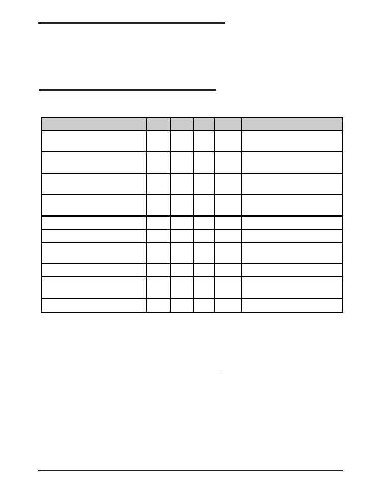
ORDERING INFORMATION
Sipex Corporation
Headquarters and
Sales Office
233 South Hillview Drive
Milpitas, CA 95035
TEL: (408) 934-7500
FAX: (408) 935-7600
Available in lead free packaging only.
/TR = Tape and Reel
Pack quantity is 3,000 for SC-70 and 2,500 for SOT-23.
Part Number Temperature Range Voltage Option
Package Type
SP6222EC5-2-5-L ..... ... ........... -40įC to +125įC ................ 2.5V .......... (Lead Free) 5 Pin SC70
SP6222EC5-2-5-L/TR ............... -40įC to +125įC ................ 2.5V ........... (Lead Free) 5 Pin SC70
SP6222EC5-3-0-L ..................... -40įC to +125įC ................ 3.0V .......... (Lead Free) 5 Pin SC70
SP6222EC5-3-0-L/TR ............... -40įC to +125įC ................ 3.0V ........... (Lead Free) 5 Pin SC70
SP6222EC5-L ........................... -40įC to +125įC ................ ADJ ........... (Lead Free) 5 Pin SC70
SP6222EC5-L/TR ..................... -40įC to +125įC ................ ADJ .......... (Lead Free) 5 Pin SC70
SP6222EK-2-5-L ....................... -40įC to +125įC ................ 2.5V .......... (Lead Free) 5 Pin SOT-23
SP6222EK-2-5-L/TR ................. -40įC to +125įC ................ 2.5V .......... (Lead Free) 5 Pin SOT-23
SP6222EK-3-0-L ....................... -40įC to +125įC ................ 3.0V .......... (Lead Free) 5 Pin SOT-23
SP6222EK-3-0-L/TR. ................ -40įC to +125įC ................ 3.0V .......... (Lead Free) 5 Pin SOT-23
SP6222EK-L ............................. -40įC to +125įC ................ ADJ .......... (Lead Free) 5 Pin SOT-23
SP6222EK-L/TR ....................... -40įC to +125įC ................ ADJ .......... (Lead Free) 5 Pin SOT-23
SP6223EC5-L ........................... -40įC to +125įC ................ ADJ ........... (Lead Free) 5 Pin SC70
SP6223EC5-L/TR ... ....... ......... -40įC to +125įC ................ ADJ .......... (Lead Free) 5 Pin SC70
SP6223EK-L ............................. -40įC to +125įC ................ ADJ .......... (Lead Free) 5 Pin SOT-23
SP6223EK-L/TR ....................... -40įC to +125įC ................ ADJ .......... (Lead Free) 5 Pin SOT-23