 | –≠–ª–µ–∫—Ç—Ä–æ–Ω–Ω—ã–π –∫–æ–º–ø–æ–Ω–µ–Ω—Ç: SP6642/3 | –°–∫–∞—á–∞—Ç—å:  PDF PDF  ZIP ZIP |
Rev. 10-6-00
SP6642/6643 High Efficiency Step-Up DC-DC Converter © Copyright 2000 Sipex Corporation
1
s
20mA Output Current at 1.2V Input
s
+2V to +5.5V Output Range
s
0.85V Guaranteed Start-Up
s
83% High Efficiency
s
1.5
µ
A Quiescent Supply Current at V
BATT
s
Reverse Battery Protection
s
Internal Synchronous Rectifier
s
5nA Logic Controlled Shutdown Current
From V
BATT
For The SP6642
s
Low-Battery Detection Active LOW
Output For The SP6643
s
Extremely Small
µ
SOIC Package
s
Pin-to-pin Compatible With MAX1642
And MAX1643
SP6642/6643
DESCRIPTION
The SP6642/6643 devices are high-efficiency, low-power step-up DC-DC converters for +1V
inputs ideal for single alkaline cell applications such as pagers, remote controls, and other
low-power portable end products. Designers can control the SP6642 device with a 1nA active
LOW shutdown input. The SP6643 features an active LOW output for low-battery conditions.
Both devices contain a 0.8
synchronous rectifier, an oscillator, a 0.6
N-channel MOSFET
power switch, an internal voltage reference, circuitry for pulse-frequency-modulation, and an
under voltage comparator. The output voltage for the SP6642/6643 devices is preset to
+3.3V + 4% or can be adjusted from +2V to +5.5V by manipulating two external resistors.
V
OUT
GND
PFI
V
BATT
LX
1
2
3
4
5
6
7
8
SP6642
PFO
SHDN
FB
V
OUT
GND
PFI
V
BATT
LX
1
2
3
4
5
6
7
8
SP6643
FB
BATTLO
PFO
Single Alkaline Cell, High Efficiency
Step-Up DC-DC Converter
Æ

Rev. 10-6-00
SP6642/6643 High Efficiency Step-Up DC-DC Converter © Copyright 2000 Sipex Corporation
2
R
E
T
E
M
A
R
A
P
.
N
I
M
.
P
Y
T
.
X
A
M
S
T
I
N
U
S
N
O
I
T
I
D
N
O
C
V
,
e
g
a
t
l
o
V
t
u
p
n
I
g
n
i
t
a
r
e
p
O
m
u
m
i
n
i
M
)
N
I
M
(
T
T
A
B
2
.
0
V
R
L
k
3
=
V
,
e
g
a
t
l
o
V
t
u
p
n
I
g
n
i
t
a
r
e
p
O
m
u
m
i
x
a
M
)
X
A
M
(
T
T
A
B
5
6
.
1
V
V
(
e
g
a
t
l
o
V
t
u
p
n
I
p
U
-
t
r
a
t
S
T
T
A
B
2
E
T
O
N
,
)
5
8
.
0
5
7
.
0
V
R
L
k
3
=
T
,
B
M
A
5
2
+
=
O
C
V
(
e
g
a
t
l
o
V
t
u
p
n
I
p
U
-
t
r
a
t
S
T
T
A
B
t
n
e
i
c
i
f
f
e
o
C
e
r
u
t
a
r
e
p
m
e
T
,
)
2
-
/
V
m
O
C
e
g
a
t
l
o
V
t
u
p
n
I
N
D
H
S
V
L
I
V
H
I
0
8
0
2
%
V
f
o
%
T
T
A
B
e
h
t
r
o
f
2
4
6
6
P
S
V
f
o
%
T
T
A
B
e
h
t
r
o
f
2
4
6
6
P
S
t
n
e
r
r
u
C
t
u
p
n
I
N
D
H
S
0
1
A
n
2
4
6
6
P
S
t
n
e
r
r
u
C
t
u
p
n
I
B
F
0
1
A
n
V
B
F
V
3
.
1
=
V
,
e
g
a
t
l
o
V
t
e
S
B
F
B
F
5
1
2
.
1
2
6
2
.
1
9
0
3
.
1
V
k
c
a
b
d
e
e
f
l
a
n
r
e
t
x
e
t
n
e
r
r
u
C
t
u
p
n
I
I
F
P
0
1
A
n
V
I
F
P
V
m
0
5
6
=
e
g
a
t
l
o
V
p
i
r
T
I
F
P
0
9
5
4
1
6
2
3
6
V
m
%
1
=
s
i
s
e
r
e
t
s
y
h
,
I
F
P
g
n
il
l
a
f
e
g
a
t
l
o
V
p
i
r
T
O
L
T
T
A
B
6
9
.
0
0
0
.
1
4
0
.
1
V
V
T
U
O
,
%
2
=
s
i
s
e
r
e
t
s
y
h
,
V
3
.
3
=
3
4
6
6
P
S
V
,
e
g
a
t
l
o
V
t
u
p
t
u
O
T
U
O
6
1
.
3
0
3
.
3
4
4
.
3
V
V
B
F
V
1
.
0
<
e
g
n
a
R
e
g
a
t
l
o
V
t
u
p
t
u
O
0
.
2
5
.
5
V
k
c
a
b
d
e
e
f
l
a
n
r
e
t
x
e
e
c
n
a
t
s
i
s
e
R
-
n
O
l
e
n
n
a
h
C
-
N
6
.
0
5
.
1
V
T
U
O
V
3
.
3
=
e
c
n
a
t
s
i
s
e
R
-
n
O
l
e
n
n
a
h
C
-
P
8
.
0
2
.
2
V
T
U
O
V
3
.
3
=
e
g
a
t
l
o
V
e
d
o
i
D
-
h
c
t
a
C
l
e
n
n
a
h
C
-
P
8
.
0
V
I
E
D
O
I
D
f
f
o
h
c
t
i
w
s
l
e
n
n
a
h
C
-
P
,
A
m
0
0
1
=
ABSOLUTE MAXIMUM RATINGS
These are stress ratings only and functional operation
of the device at these ratings or any other above those
indicated in the operation sections of the specifications
below is not implied. Exposure to absolute maximum
rating conditions for extended periods of time may
affect reliability.
V
BATT
to GND.............................................-0.3 to 6.0V
V
OUT
to GND..............................................-0.3 to 6.0V
LX, SHDN, FB, BATTLO, PFO to GND....-0.3 to 6.0V
PFI to GND...............................................-0.3 to 6.0V
Reverse battery Current, T
AMB
=+25
O
C.............220mA
(NOTE 1)
V
BATT
forward current............................................0.5A
V
OUT
, LX current......................................................1A
Storage Temperature Range............-65∞C to +165∞C
Lead Temperature (soldering 10s)..................+300∞C
Operating Temperature.......................-40∞C to +85∞C
Power Dissipation Per Package
8-pin
µ
SOIC
(derate 4.85mW/
O
C above +70
O
C)
..........390mW
SPECIFICATIONS
V
BATT
= V
SHDN
= 1.3V, I
LOAD
= 0mA, FB = GND, T
AMB
= -40
O
C to +85
O
C, and typical values are at T
AMB
= +25
O
C unless otherwise noted.

Rev. 10-6-00
SP6642/6643 High Efficiency Step-Up DC-DC Converter © Copyright 2000 Sipex Corporation
3
SPECIFICATIONS (continued)
V
BATT
= V
SHDN
= 1.3V, I
LOAD
= 0mA, FB = GND, T
AMB
= -40
O
C to +85
O
C, and typical values are at T
AMB
= +25
O
C unless otherwise noted.
R
E
T
E
M
A
R
A
P
.
N
I
M
.
P
Y
T
.
X
A
M
S
T
I
N
U
S
N
O
I
T
I
D
N
O
C
V
o
t
n
i
t
n
e
r
r
u
C
t
n
e
c
s
e
i
u
Q
T
U
O
I
,
T
U
O
Q
3
1
0
2
µ
A
V
T
U
O
V
5
.
3
=
V
o
t
n
i
t
n
e
r
r
u
C
t
n
e
c
s
e
i
u
Q
T
T
A
B
I
,
T
T
A
B
Q
5
.
1
5
.
2
µ
A
V
T
T
A
B
V
0
.
1
=
V
o
t
n
i
t
n
e
r
r
u
C
n
w
o
d
t
u
h
S
T
U
O
I
,
T
U
O
N
D
H
S
1
0
0
.
0
5
.
0
µ
A
V
T
U
O
e
h
t
r
o
f
V
5
.
3
=
2
4
6
6
P
S
V
o
t
n
i
t
n
e
r
r
u
C
n
w
o
d
t
u
h
S
T
T
A
B
I
,
T
T
A
B
N
D
H
S
5
0
0
.
0
1
.
0
µ
A
V
T
T
A
B
e
h
t
r
o
f
V
0
.
1
=
2
4
6
6
P
S
V
,
O
L
T
T
A
B
d
n
a
O
F
P
r
o
f
e
g
a
t
l
o
V
t
u
p
t
u
O
w
o
L
L
O
4
.
0
V
V
I
F
P
V
,
V
0
=
T
U
O
I
,
V
3
.
3
+
=
K
N
I
S
A
m
1
=
O
L
T
T
A
B
d
n
a
O
F
P
r
o
f
t
n
e
r
r
u
C
e
g
a
k
a
e
L
1
µ
A
V
I
F
P
V
,
V
m
0
5
6
=
O
F
P
V
6
=
e
g
a
t
l
o
V
p
i
r
T
O
L
T
T
A
B
6
9
.
0
0
.
1
4
0
.
1
V
V
T
U
O
e
h
t
r
o
f
%
2
=
s
i
s
e
r
e
t
s
y
h
,
V
3
.
3
+
=
3
4
6
6
P
S
K
,
t
n
a
t
s
n
o
C
e
m
i
T
-
n
O
7
1
5
2
5
3
-
V
µ
s
V
<
V
9
.
0
T
T
A
B
t
(
V
5
.
1
<
N
O
V
/
K
=
T
T
A
B
)
)
3
E
T
O
N
(
o
i
t
a
R
g
n
i
k
c
a
r
T
e
m
i
T
-
f
f
O
1
5
.
1
V
<
V
9
.
0
T
T
A
B
V
,
V
5
.
1
<
T
U
O
V
3
.
3
+
=
y
c
n
e
i
c
i
f
f
E
3
8
%
I
D
A
O
L
A
m
0
2
=
NOTE 1: The reverse battery current is measured from the Typical Operating Circuit's input terminal to GND
when the battery is connected backward. A reverse current of 220mA will not exceed package dissipation limits
but, if left for an extended time (more than 10 minutes), may degrade performance.
NOTE 2: Start-up guaranteed by correlation to measurements of device parameters (i.e. switch on-resistance,
on-times, and output voltage trip points.
NOTE 3: tOFF = Ratio x
. This guarantees discontinous condition.
NOTE 4: Specifications to -40∫C are guaranteed by design, not production tested.
t
ON
x V
BATT
V
OUT
- V
BATT

Rev. 10-6-00
SP6642/6643 High Efficiency Step-Up DC-DC Converter © Copyright 2000 Sipex Corporation
4
0
10
20
30
40
50
60
70
80
90
100
0.01
0.1
1
10
100
Output Current (mA)
Vin = 1.6V
Vin = 1.2V
Vin = 1.0V
Vin = 0.85V
Efficienc
y (%)
0
10
20
30
40
50
60
70
80
90
100
0.01
0.1
1
10
100
Output Current (mA)
Vin = 1.6V
Vin = 1.2V
Vin = 1.0V
Vin = 0.85V
Efficienc
y (%)
0
10
20
30
40
50
60
70
80
90
100
0.01
0.1
1
10
100
Output Current (mA)
Vin = 1.6V
Vin = 1.2V
Vin = 1.0V
Vin = 0.85V
Efficienc
y (%)
0
10
20
30
40
50
60
70
80
90
100
0.01
0.1
1
10
100
Output Current (mA)
Vin = 1.6V
Vin = 1.2V
Vin = 1.0V
Vin = 0.85V
Efficienc
y (%)
Figure 1. Efficiency vs. Output Current (V
OUT
=2.4V)
where L1=100
µ
H, Sumida CD54-101
Figure 2. Efficiency vs. Output Current (V
OUT
=2.4V)
where L1=150
µ
H, TDK NLC565050T-151K
Figure 3. Efficiency vs. Output Current (V
OUT
=3.3V)
where L1=100
µ
H, Sumida CD54-101
Figure 4. Efficiency vs. Output Current (V
OUT
=3.3V)
where L1=150
µ
H, TDK NLC565050T-151K
PERFORMANCE CHARACTERISTICS
Refer to the circuit in
Figure 25 with V
BATT
= 1.2V, R1 + R2 = 1M
, and T
AMB
= +25
O
C unless otherwise noted.

Rev. 10-6-00
SP6642/6643 High Efficiency Step-Up DC-DC Converter © Copyright 2000 Sipex Corporation
5
0
20
40
60
80
100
-40
-20
0
20
40
60
80
100
Temperature (oC)
Quiescent Current (
µ
A)
10
100
1000
10000
0.8
1.0
1.2
1.4
1.6
1.8
Input Voltage (V)
Vout = 5.0V
Vout = 3.3V
Vout = 2.4V
Quiescent Current (
µ
A)
0
10
20
30
40
50
60
70
80
90
100
0.01
0.1
1
10
100
Output Current (mA)
Vin = 1.6V
Vin = 1.2V
Vin = 1.0V
Vin = 0.85V
Efficienc
y (%)
0
10
20
30
40
50
60
70
80
90
100
0.01
0.1
1
10
100
Output Current (mA)
Vin = 1.6V
Vin = 1.2V
Vin = 1.0V
Vin = 0.85V
Efficienc
y (%)
Figure 5. Efficiency vs. Output Current (V
OUT
=5.0V)
where L1=100
µ
H, Sumida CD54-101
Figure 6. Efficiency vs. Output Current (V
OUT
=5.0V)
where L1=150
µ
H, TDK NLC565050T-151K
Figure 7. No-Load Battery Current vs. Input voltage
Figure 8. No-Load Battery Current vs. Temperature
Where V
BATT
= 1.2V, V
OUT
= 3.3V
PERFORMANCE CHARACTERISTICS (continued)
Refer to the circuit in
Figure 25 with V
BATT
= 1.2V, R1 + R2 = 1M
, and T
AMB
= +25
O
C unless otherwise noted.

Rev. 10-6-00
SP6642/6643 High Efficiency Step-Up DC-DC Converter © Copyright 2000 Sipex Corporation
6
Figure 9. V
BATT
and V
OUT
Pin Quiescent Currents vs.
Temperature where V
BATT
= 1.2V, V
OUT
= 3.6V
Figure 10. Minimum Start-Up Input Voltage vs. Output
Current where L1=100
µ
H, Sumida CD54-101
Figure 11. Minimum Start-Up Input Voltage vs. Output
Current where L1=150
µ
H, TDK NLC565050T-151K
Figure 12. Maximum Output Current vs. Input Voltage
where L1=100
µ
H, Sumida CD54-101
PERFORMANCE CHARACTERISTICS (continued)
Refer to the circuit in
Figure 25 with V
BATT
= 1.2V, R1 + R2 = 1M
, and T
AMB
= +25
O
C unless otherwise noted.
0.6
0.7
0.8
0.9
1.0
1.1
1.2
1.3
1.4
1.5
1.6
0
5
10
15
20
25
30
Output Current (mA)
Vout = 5V
Vout = 3.3V
Vout = 2.4V
Star
t-Up Input
V
olta
g
e
(V)
0.6
0.7
0.8
0.9
1.0
1.1
1.2
1.3
1.4
1.5
1.6
0
2
4
6
8
10
12
14
16
Output Current (mA)
Vout = 5V
Vout = 3.3V
Vout = 2.4V
Star
t-Up Input
V
olta
g
e
(V)
0
5
10
15
20
25
30
35
40
0.8 0.9 1.0 1.1 1.2 1.3 1.4 1.5 1.6
Vout = 2.4V
Vout = 3.3V
Vout = 5V
Input Voltage (V)
Maxim
um Output Current (mA
)
0
5
10
15
20
25
30
35
40
-40 -20
0
20
40
60
80
100
Temperature (oC)
Iout
Ibatt
Quiescent Current (
µ
A)

Rev. 10-6-00
SP6642/6643 High Efficiency Step-Up DC-DC Converter © Copyright 2000 Sipex Corporation
7
Figure 13. Maximum Output Current vs. Input Voltage
where L1=150
µ
H, TDK NLC565050T-151K
Figure 14. Switching Waveforms:
V
OUT
=3.3V, V
IN
=1.2V, I
OUT
=12mA where
1: LX, 2V/div, L1=TDK NKLC565050T-151K
2: V
OUT
, 20mV/div, 3.3V DC offset
3: Inductor Current, 100mA/div
Figure 15. Load-Transient Response:
V
OUT
=3.3V, V
BATT
=1.2V where
1: V
OUT
, 20mV/div, 3.3V DC offset
2: LOAD, 2mA to 20mA, 10mA/div
Figure 16. Line-Transient Response:
V
OUT
=3.3V, LOAD=15mA where
1: V
OUT
, 50mV/div, 3.3V DC offset
2: V
BATT
, 1V to 5V, 500mV/div
PERFORMANCE CHARACTERISTICS (continued)
Refer to the circuit in
Figure 25 with V
BATT
= 1.2V, R1 + R2 = 1M
, and T
AMB
= +25
O
C unless otherwise noted.
0
2
4
6
8
10
12
14
16
18
20
22
0.8 0.9 1.0 1.1 1.2 1.3 1.4 1.5 1.6
Input Voltage (V)
Vout = 2.4V
Vout = 3.3V
Vout = 5V
Maxim
um Output Current (mA)
10msec/div
500
µ
sec/div
500
µ
sec/div

Rev. 10-6-00
SP6642/6643 High Efficiency Step-Up DC-DC Converter © Copyright 2000 Sipex Corporation
8
E
M
A
N
N
O
I
T
C
N
U
F
R
E
B
M
U
N
N
I
P
2
4
6
6
P
S
3
4
6
6
P
S
V
T
T
A
B
e
h
t
r
o
F
.
y
l
p
p
u
S
y
r
e
t
t
a
B
3
4
6
6
P
S
e
h
t
f
o
t
u
p
n
i
r
o
s
n
e
s
e
h
t
o
t
s
e
i
t
n
i
p
s
i
h
t
,
.
r
o
t
a
r
a
p
m
o
c
O
L
T
T
A
B
1
1
I
F
P
s
k
n
i
s
O
F
P
,
V
m
4
1
6
w
o
l
e
b
s
p
o
r
d
I
F
P
n
o
e
g
a
t
l
o
v
e
h
t
n
e
h
W
.
t
u
p
n
I
li
a
F
-
r
e
w
o
P
.
t
n
e
r
r
u
c
2
2
O
L
T
T
A
B
V
t
a
e
g
a
t
l
o
v
e
h
t
n
e
h
W
.
t
u
p
t
u
O
W
O
L
-
y
r
e
t
t
a
B
n
i
a
r
D
-
n
e
p
O
T
T
A
B
w
o
l
e
b
s
p
o
r
d
.
t
n
e
r
r
u
c
s
k
n
i
s
O
L
T
T
A
B
,
V
1
-
3
O
F
P
w
o
l
e
b
s
p
o
r
d
I
F
P
n
e
h
w
t
n
e
r
r
u
c
s
k
n
i
S
.
t
u
p
t
u
O
li
a
F
-
r
e
w
o
P
n
i
a
r
D
-
n
e
p
O
.
V
m
4
1
6
3
4
N
D
H
S
V
o
t
t
c
e
n
n
o
C
.
t
u
p
n
I
n
w
o
d
t
u
h
S
W
O
L
-
e
v
i
t
c
A
T
T
A
B
.
n
o
i
t
a
r
e
p
o
l
a
m
r
o
n
r
o
f
4
-
B
F
t
u
p
n
i
s
i
h
t
t
c
e
n
n
o
C
.
n
o
i
t
a
r
e
p
o
t
u
p
t
u
o
-
e
l
b
a
t
s
u
j
d
a
r
o
f
t
u
p
n
I
.
t
u
p
n
I
k
c
a
b
d
e
e
F
V
n
e
e
w
t
e
b
r
e
d
i
v
i
d
e
g
a
t
l
o
v
r
o
t
s
i
s
e
r
l
a
n
r
e
t
x
e
n
a
o
t
n
i
p
T
U
O
t
c
e
n
n
o
C
.
D
N
G
d
n
a
.
n
o
i
t
a
r
e
p
o
t
u
p
t
u
o
-
d
e
x
i
f
r
o
f
D
N
G
o
t
5
5
D
N
G
.
d
n
u
o
r
g
y
ll
a
c
i
p
y
t
,
l
a
i
t
n
e
t
o
p
t
i
u
c
r
i
c
t
s
e
w
o
l
e
h
t
o
t
t
c
e
n
n
o
C
6
6
X
L
V
m
o
r
f
d
e
t
c
e
n
n
o
c
s
i
r
o
t
c
u
d
n
i
n
A
.
li
o
C
T
T
A
B
h
c
t
i
w
s
T
E
F
S
O
M
l
e
n
n
a
h
C
-
N
e
h
t
o
t
.
n
i
p
s
i
h
t
h
g
u
o
r
h
t
n
i
a
r
d
r
e
i
f
i
t
c
e
r
-
s
u
o
n
o
r
h
c
n
y
s
l
e
n
n
a
h
C
-
P
e
h
t
d
n
a
n
i
a
r
d
7
7
V
T
U
O
.
t
u
p
n
i
r
e
w
o
p
C
I
d
n
a
n
o
i
t
a
r
e
p
o
V
3
.
3
d
e
x
i
f
r
o
f
t
u
p
n
i
k
c
a
b
d
e
e
F
.
t
u
p
t
u
O
r
e
w
o
P
V
o
t
e
s
o
l
c
r
o
t
i
c
a
p
a
c
r
e
t
li
f
t
c
e
n
n
o
C
T
U
O
.
8
8
Figure 17. Shutdown Response and Inductor Current:
V
OUT
=3.3V, V
BATT
=1.2V, I
OUT
=5mA where
1: V
OUT
, 1V/div
2: SHDN, 2v/div
3: Inductor Current, 200mA/div
Table 1. SP6642/6643 Pin Descriptions
PERFORMANCE CHARACTERISTICS (continued)
Refer to the circuit in
Figure 25 with V
BATT
= 1.2V, R1 + R2 = 1M
, and T
AMB
= +25
O
C unless otherwise noted.
10msec/div

Rev. 10-6-00
SP6642/6643 High Efficiency Step-Up DC-DC Converter © Copyright 2000 Sipex Corporation
9
V
OUT
GND
PFI
V
BATT
LX
1
2
3
4
5
6
7
8
SP6642
PFO
SHDN
FB
V
OUT
GND
PFI
V
BATT
LX
1
2
3
4
5
6
7
8
SP6643
FB
BATTLO
PFO
Figure 18. Pinout for the SP6642
Figure 19. Pinout for the SP6643

Rev. 10-6-00
SP6642/6643 High Efficiency Step-Up DC-DC Converter © Copyright 2000 Sipex Corporation
10
DESCRIPTION
The SP6642/6643 devices are high-efficiency,
low-power step-up DC-DC converters ideal for
single alkaline cell applications such as pagers,
remote controls, and other low-power portable
end products.
The SP6642 features a 5nA logic-controlled
shutdown mode. The SP6643 features dedicated
low-battery detector circuitry. Both devices
contain a 0.8
synchronous rectifier, an
oscillator, a 0.6
N-channel MOSFET power
switch, an internal voltage reference, circuitry
for pulse-frequency-modulation, and an under
voltage comparator. The output voltage for the
SP6642/6643 devices can be adjusted from +2V
to +5.5V by manipulating two external resistors.
The output voltage is preset to +3.3V.
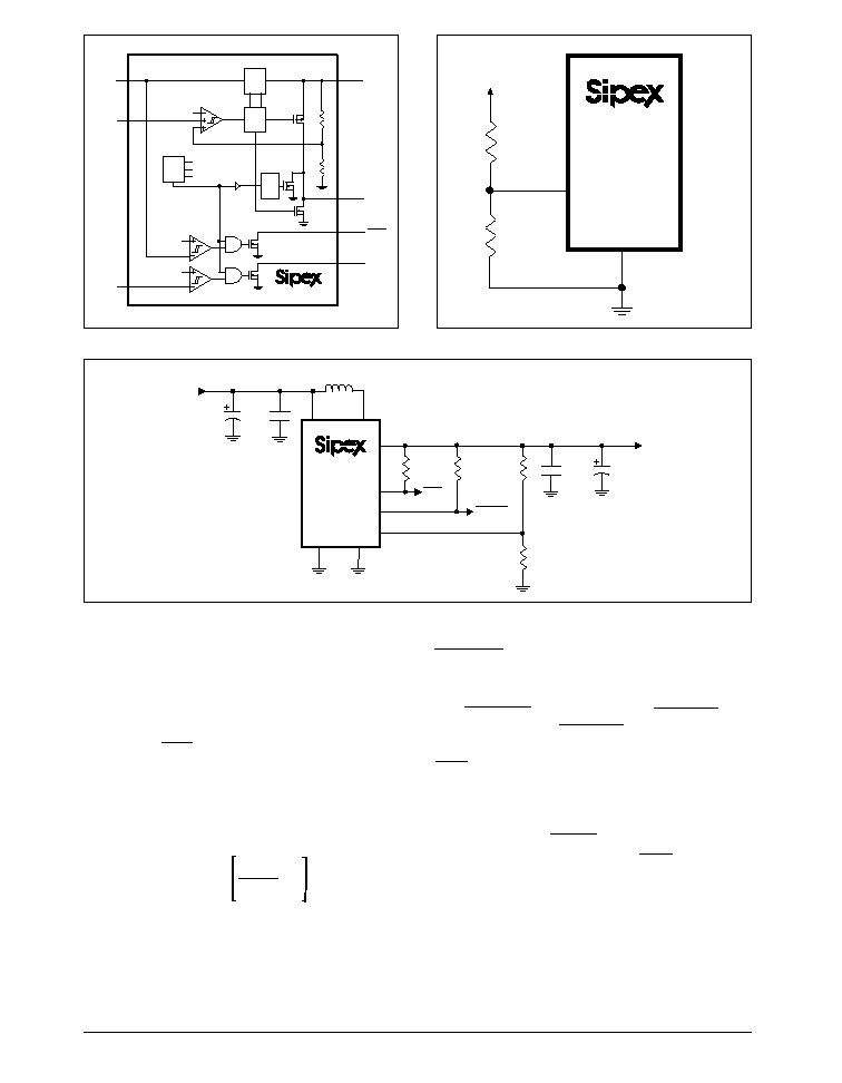
THEORY OF OPERATION
The SP6642/6643 devices are ideal for end
products that function with a single alkaline cell,
such as remote controls, pagers, and other portable
consumer products. Designers can implement
the SP6642/6643 devices into applications with
the following power management operating
states: 1. where the primary battery is good and
the load is active, and 2. where the primary
battery is good and the load is sleeping.
In the first operating state where the primary
supply is good and the load is active, the SP6642/
6643 devices typically offer 80% efficiency,
drawing tens of milliamps.
Applications will predominantly operate in the
second state where the primary supply is good
and the load is sleeping. The SP6642/6643
devices draw a very low quiescent current while
the load in its disabled state will draw typically
hundreds of microamps.
The pulse-frequency-modulation (PFM) circuitry
provides higher efficiencies at low to moderate
output loads than traditional PWM converters
are capable of delivering.
The on-time and minimum off-times are varied
as a function of the input and output voltages:
t
ON
=
K
V
BATT
t
OFF(MIN)
=
1.2 x K
V
OUT
- V
BATT
where t
ON
is the on-time, K is the on-time constant
typically 25V-
µ
s, V
BATT
is the supply voltage,
t
OFF(MIN)
is the minimum off-time, and V
OUT
is the
output voltage. This allows the SP6642/6643
devices to maintain a high efficiency over a
wide range of loads and input/output voltages.
The DC-DC converter is powered from V
OUT
.
In a state where the error comparator detects that
the output voltage at V
OUT
is too low, the internal
N-channel MOSFET switch is turned on until
the on-time is satisfied. Refer to Figures 20, 21,
22 and 23. During the on-time, current ramps up
in the inductor, storing energy in a magnetic
field. When the MOSFET turns off, during the
second half of each cycle the magnetic field
collapses. This causes the inductor voltage to
force current through the synchronous rectifier
transferring the stored energy from the inductor
to the output filter capacitor and the load. The
output filter capacitor stores charge while current
from the inductor is high and holds the output
voltage high until the second half of the next
switching cycle, smoothing power flow to the
load.
Internal Bootstrap Circuitry
The internal bootstrap circuitry contains a
low-voltage start-up oscillator that pumps up
the output voltage to approximately 1.9V so the
main DC-DC converter can function. At lower
battery supply voltages, the circuitry can start
up with low-load conditions. Designers can
reduce the load as needed to allow start-up with
input voltages below 1V. Refer to Figures 10 to
13. Once started, the output voltage can maintain
the load as the battery voltage decreases below
the initial start-up voltage. The start-up oscillator
is powered by V
BATT
driving a charge pump and
NMOS switch. During start-up, the P-channel
synchronous rectifier remains off and either its
body diode or an external diode is used as an
output rectifier.

Rev. 10-6-00
SP6642/6643 High Efficiency Step-Up DC-DC Converter © Copyright 2000 Sipex Corporation
11
Figure 20. Internal Block Diagram of the SP6642
GND
OUT
0.1
µ
F
FB
LX
V
BATT
22
µ
F
0.1
µ
F
22
µ
F
PFI
+3.3V
OUT
SHDN
100
µ
H
350mA
0.85V to
1.65V Input
SP6642
PFO
Figure 21. SP6642 +3.3V Typical Application Circuit
TIMING
SHDN
LOGIC
T-OFF
T-ON
DRV-P
DRV-N
EN
V
REF
FB
V
BATT
P
V
OUT
LX
V
REF
0.5V
REF
V
REF
V
OUT
1.9V
0.5V
REF
PFI
PFO
START
UP
OSC
N
SP6642
N
Rev. 10-6-00
SP6642/6643 High Efficiency Step-Up DC-DC Converter © Copyright 2000 Sipex Corporation
12
GND
OUT
0.1
µ
F
FB
LX
V
BATT
22
µ
F
0.1
µ
F
22
µ
F
+3.3V
OUT
100
µ
H
350mA
0.85V to
1.65V Input
SP6643
PFO
PFI
BATTLO
Figure 23. SP6643 +3.3V Typical Application Circuit
TIMING
LOGIC
T-OFF
T-ON
DRV-P
DRV-N
EN
V
REF
FB
V
BATT
P
V
OUT
LX
V
REF
0.5V
REF
V
REF
START
UP
OSC
N
N
0.5V
REF
PFI
PFO
1.0V
BATTLO
SP6643
1.0V
Figure 22. Internal block diagram of the SP6643
R4
R3
GND
PFI
V
TH
SP6642
Figure 24. Power-Fail Detection Circuitry
Power-Fail Detection Circuitry
The SP6642/6643 devices have an internal
comparator for power-fail detection. This
comparator can detect a loss of power at the
input or output. If the voltage at PFI falls below
614mV, the PFO output sinks current to ground.
Hysteresis at the power-fail input is 1%. The
power-fail monitor's threshold voltage is
determined by two resistors, R3 and R4. Refer
to Figure 24. The power-fail monitor threshold
voltage can be set using the following equation:
where R3 and R4 are the resistors in Figure 24,
V
TH
is the desired threshold voltage of the power-
fail detector, and V
PFI
is the 614mV reference of
the power-fail comparator. Since PFI leakage is
10nA max, select feedback resistor R4 in the
100k
to 1M
.
BATTLO for the SP6643
The SP6643 device has an internal comparator
for low-battery detection. If V
BATT
drops below
1V, BATTLO will sink current. BATTLO is an
open-drain output. BATTLO used in conjunction
with the power-fail detection circuitry (PFI/
PFO) will monitor both the input and output
voltages.
Shutdown for the SP6642
A logic LOW at SHDN will drive the SP6642
into a shutdown mode where PFO goes into a
high-impedance state, the internal switching
MOSFET turns off, and the synchronous rectifier
turns off to prevent reverse current from flowing
from the output back to the input. Designers
should note that in shutdown, the output can
drift to one diode drop below V
BATT
because
there is still a forward current path through the
R3 = R4 x -1
V
TH
V
PFI

Rev. 10-6-00
SP6642/6643 High Efficiency Step-Up DC-DC Converter © Copyright 2000 Sipex Corporation
13
synchronous-rectifier body diode from the input
to the output. To disable the shutdown feature,
designers can connect SHDN to V
BATT
.
Adjustable Output Voltage
Driving FB to ground (logic LOW) will drive
the output voltage to the fixed-voltage operation
of +3.3V + 4%. Connecting FB to a voltage
divider between V
OUT
and ground will select an
adjustable output voltage between +2V and
+5.5V. Refer to Figure 25. FB regulates to
+1.23V.
Since the FB leakage current is 10nA maximum,
designers should select the feedback resistor R2
in the 100k
to 1M
range. R1 can be
determined with the following equation:
R1 = R2 x -1
V
OUT
V
REF
where R3 and R4 are the feedback resistors in
Figure 25, V
OUT
is the output voltage, and V
REF
is 1.23V.
Battery Reversal Protection
The SP6642/6643 devices will tolerate single-
cell battery reversal up to the package power-
dissipation limits noted in the
ABSOLUTE
MAXIMUM RATINGS
section. An internal
GND
V
OUT
0.1
µ
F
FB
LX
V
BATT
22
µ
F
0.1
µ
F
22
µ
F
PFI
V
OUT
=
2V to 5.2V
SHDN
100
µ
H
350mA
0.88V to
1.65V Input
SP6642
PFO
100pF*
R1
R2
*optional compensation
Figure 25. Adjustable Output Voltage Circuitry
diode in series with an internal 5
resistor limits
any reverse current to less than 220mA
preventing damage to the devices. Prolonged
operation above 220mA reverse-battery current
can degrade performance of the devices.
The Inductor
It is recommended that designers implement a
100
µ
H inductor for typical application of the
SP6642/6643 devices. Lower inductor values
down to 68
µ
H will increase the maximum
output current. Higher inductor values up to
220
µ
H will reduce peak inductor current and
any consequent ripple and noise. The saturation-
current rating of the inductor selected must
exceed the peak current limit synthesized by the
SP6642/6643 devices' timing algorithms. This
can be calculated with the following equation:
I
PEAK
= K
MAX
L
MIN
where I
PEAK
is the peak current, K
MAX
is 35V-
µ
s,
and L
MIN
is the minimum inductance selected.
The maximum recommended I
PEAK
is 350mA.
To optimize efficiency, select an inductor with
a series resistance less than 1
.
Table 1 lists surface mount inductor information
for the user, including series resistance and
saturation current rating.

Rev. 10-6-00
SP6642/6643 High Efficiency Step-Up DC-DC Converter © Copyright 2000 Sipex Corporation
14
It is suggested designers select the largest
inductor value possible that will satisfy the load
requirement and minimize peak switching
current and any resultant noise and voltage
ripple. A closed-core inductor, such as a toroid
or shielded bobbin, will minimize any fringe
magnetic fields or EMI.
APPLICATION NOTES
Printed circuit board layout is a critical part of
design. Poor designs can result in excessive
EMI on the voltage gradients and feedback
paths on the ground planes with applications
involving high switching frequencies and large
peak currents. Excessive EMI can result in
instability or regulation errors.
All power components should be placed on the
PC board as closely as possible with the traces
kept short, direct, and wide (>50mils or 1.25mm).
Extra copper on the PC board should be integrated
into ground as a pseudo-ground plane. On a
multilayer PC board, route the star ground using
component-side copper fill, then connect it to
the internal ground plane using vias.
For the SP6642/6643 devices, the inductor and
input and output filter capacitors should be
soldered with their ground pins as close together
as possible in a star-ground configuration. The
V
OUT
pin must be bypassed directly to ground as
close to the SP6642/6643 devices as possible
(within 0.2in or 5mm). The DC-DC converter
and any digital circuitry should be placed on the
opposite corner of the PC board as far away
from sensitive RF and analog input stages. The
external voltage-feedback network should be
placed very close to the FB pin (within 0.2in or
5mm). Any noisy traces, such as from the LX
pin, should be kept away from the voltage-
feedback network and separated from it using
grounded copper to minimize EMI.
Capacitor equivalent series resistance is a major
contributor to output ripple, usually greater than
60%. Low ESR capacitors are recommended.
Ceramic capacitors have the lowest ESR.
Low-ESR tantalum capacitors may be a more
acceptable solution having both a low ESR and
lower cost than ceramic capacitors. Designers
should select input and output capacitors with a
rating exceeding the peak inductor current. Do
not allow tantalum capacitors to exceed their
ripple-current ratings. A 22
µ
F, 6V, low-ESR,
surface-mount tantalum output filter capacitor
typically provides 60mV output ripple when
stepping up from 1.3V to 3.3V at 20mA. An
input filter capacitor can reduce peak currents
drawn from the battery and improve efficiency.
Low-ESR aluminum electrolytic capacitors are
acceptable in some applications but standard
aluminum electrolytic capacitors are not
recommended.
Designers should add LC pi filters, linear
post-regulators, or shielding in applications
necessary to address excessive noise, voltage
ripple, or EMI concerns. The LC pi filter's cutoff
frequency should be at least a decade or two
below the DC-DC converters's switching
frequency for the specified load and input voltage.
INDUCTANCE
VENDOR/PART
RESISTANCE
I
SAT
(
µ
H)
(
)
(mA)
68
Coilcraft DO1608-683
0.75
400
Sumida CD54-680
0.46
610
Coilcraft DO1608-104
1.1
310
100
Sumida CD54-101
0.7
520
TDK NLC565050T-101K
1.6
250
Coilcraft DO1608-154
1.7
270
150
Sumida CD54-151
1.1
400
TDK NLC565050T-151K
2.2
210
220
Coilcraft DO1608-224
2.3
220
Sumida CD54-221
1.57
350
INDUCTOR SPECIFICATION
Table 1. Surface-Mount Inductor Information

Rev. 10-6-00
SP6642/6643 High Efficiency Step-Up DC-DC Converter © Copyright 2000 Sipex Corporation
15
P
W
50
µ
SOIC devices per tube
8-pin
µ
SOIC 13" reels: P = 8mm, W = 12mm
pkg min qty per reel std qty per reel max qty per reel
EU 500 2500 3000
All package dimensions in inches
1
0.013
±
0.005
0.0256
BSC
0.118
±
0.004
0.020
2
0.020
0.116
±
0.004
0.034
±
0.004
0.040
±
0.003
0.004
±
0.002
0.118
±
0.004
0.118
±
0.004
0.037
Ref
0.0215
±
0.006
3.0∞
±
3∞
R .003
12.0∞
±
4∞
0.006
±
0.006
0.006
±
0.006
0.008
0∞ - 6∞
0.012
±
0.003
0.01
12.0∞
±
4∞
0.16
±
0.003
0.0965
±
0.003
0.116
±
0.004

Rev. 10-6-00
SP6642/6643 High Efficiency Step-Up DC-DC Converter © Copyright 2000 Sipex Corporation
16
ORDERING INFORMATION
Model
Temperature Range
Package Type
SP6642EU ............................................. -40
O
C to +85
O
C ......................................... 8-Pin
µ
SOIC
SP6643EU ............................................. -40
O
C to +85
O
C ......................................... 8-Pin
µ
SOIC
Corporation
SIGNAL PROCESSING EXCELLENCE
Sipex Corporation reserves the right to make changes to any products described herein. Sipex does not assume any liability arising out of the
application or use of any product or circuit described herein; neither does it convey any license under its patent rights nor the rights of others.
Please consult the factory for pricing and availability on a Tape-On-Reel option.
Sipex Corporation
Headquarters and
Sales Office
22 Linnell Circle
Billerica, MA 01821
TEL: (978) 667-8700
FAX: (978) 670-9001
e-mail: sales@sipex.com
Sales Office
233 South Hillview Drive
Milpitas, CA 95035
TEL: (408) 934-7500
FAX: (408) 935-7600