 | –≠–ª–µ–∫—Ç—Ä–æ–Ω–Ω—ã–π –∫–æ–º–ø–æ–Ω–µ–Ω—Ç: SP9842BS | –°–∫–∞—á–∞—Ç—å:  PDF PDF  ZIP ZIP |

267
s
Replaces 8 Potentiometers and 8 Op Amps
s
Operates from Single +5V Supply
s
6.3 MHz 2-Quadrant Multiplying Gain Band-
width
s
No Signal Inversion
s
Eight Reference Inputs, Eight Voltage
Outputs (SP9841)
s
Four Reference Inputs, Eight Voltage
Outputs (SP9842)
s
3-Wire Serial Input
s
0.8MHz Data Update Rate
s
+3.25 Volt Output Swing
s
Midscale Preset
s
Low 65 mW Power Dissipation (8
mW
/DAC)
DESCRIPTION...
The SP9841 and SP9842 are general purpose octal DACs in a single package. The SP9841
features eight individual reference inputs, while the SP9842 provides four pair of voltage
reference inputs. Both parts feature 6.3MHz bandwidth, two≠quadrant multiplication, and a
three≠wire serial interface. Other features include midscale preset, no signal inversion and low
power dissipation from a single +5V supply. Devices are available in commercial and industrial
temperature ranges.
+
≠
4
8
8
8
DAC A
8 x 8
DAC
REGISTER
SERIAL
REGISTER
LOGIC
Decoded
Address
Data
Clock
Serial Data Input
Serial Data Output
Preset
Load
V
REF
Low
SP9842
+
≠
8
DAC B
V
IN
A/B
V
OUT
B
V
OUT
A
+
≠
8
DAC G
+
≠
8
DAC H
V
IN
G/H
V
OUT
H
V
OUT
G
SP9842 Block Diagram
4
8
8
8
DAC A
DAC H
8
8 x 8
DAC
REGISTER
SERIAL
REGISTER
LOGIC
Decoded
Address
Data
Clock
Serial Data Input
Serial Data Output
Preset
Load
V
IN
A
V
OUT
A
V
IN
H
V
OUT
H
V
REF
Low
SP9841
+
≠
SP9841 Block Diagram
SP9841/42
8-Bit Octal, 2-Quadrant Multiplying, BiCMOS DAC

268
ABSOLUTE MAXIMUM RATINGS
These are stress ratings only and functional operation of the device
at these or any other above those indicated in the operation
sections of the specifications below is not implied. Exposure to
absolute maximum rating conditions for extended periods of time
may affect reliability.
V
DD
to GND ...................................................................... -0.3V, +7V
V
IN
X to GND ............................................................................... V
DD
V
REF
L to GND ............................................................................. V
DD
V
OUT
X to GND ............................................................................ V
DD
Short Circuit I
OUT
X to GND ............................................ Continuous
Digital Input & Output Voltage to GND ....................................... V
DD
Operating Temperature Range
Commercial: SP9841K/SP9842K .............................. 0
∞
C to +70
∞
C
Extended Industrial: SP9841B/SP9842B ................ -40
∞
C to +85
∞
C
Maximum Junction Temperature (T
J
max) .......................... +150
∞
C
Storage Temperature ................................................. -65
∞
to 150
∞
C
Lead Temperature (Soldering, 10 sec) ............................... +300
∞
C
Package Power Dissipation ................................. (T
J
max - T
A
)/
JA
Thermal Resistance
JA
P-DIP .................................................................................. 57
∞
C/W
SOIC-24 .............................................................................. 70
∞
C/W
SPECIFICATIONS
(V
DD
= +5V, All V
IN
X= +1.625V, V
REF
L = 0V, T
A
= 25
∞
C for commercial≠grade parts; T
MIN
T
A
= T
MAX
for industrial≠grade parts; specifications apply to
all DAC's unless noted otherwise.)
PARAMETER
MIN.
TYP.
MAX.
UNITS
CONDITIONS
SIGNAL INPUTS
Input Voltage Range
0
1.625
V
V
REFL
= GND, V
DD
= 4.75V
Input Resistance
D = 55
H
; Code Dependent
SP9841
5
10
k
SP9842
2.5
5
k
Input Capacitance
Code Dependent
SP9841
19
30
pF
SP9842
38
60
pF
V
REFL
Resistance
0.375
0.75
k
All D = AB
H
; Code Dependent
V
REFL
Capacitance
190
250
pF
Code Dependent
DIGITAL INPUTS
Logic High
2.4
V
Logic Low
0.8
V
Input Current
±
10
µ
A
Input Capacitance
8
pF
Input Coding
Binary
STATIC ACCURACY
Resolution
8
Bits
Integral Nonlinearity
±
0.25
±
1.0
LSB
Note 1
Differential Nonlinearity
±
0.2
±
1.0
LSB
Note 1
Half-Scale Output Voltage
1.600
1.625
1.650
V
PR = LOW, Sets D = 80
H
Zero-Scale Output Voltage
20
100
mV
D = 00
H
Output Voltage Drift
25
µ
V/
∞
C
PR = LOW, Sets D = 80
H
DYNAMIC PERFORMANCE
Multiplying Gain Bandwidth
4
6.3
MHz
V
IN
X = 100 mV p-p+ 1.0V dc
Slew Rate
Measured 10% to 90%
Positive
3.0
7.9
V/
µ
s
V
OUT
X = 100mV to +3.1V
Negative
≠3.0
≠8.3
V/
µ
s
V
OUT
X = +3.1V to 100mV
Total Harmonic Distortion
0.005
%
V
IN
X = 0.8V
DC
+ 1.4V p-p
D= FF
H
; 1kHz, f
LP
= 80 kHz
Output Settling Time
0.7
µ
s
±
1 LSB Error Band, 8
H
to
255
H
Crosstalk
60
70
dB
Note 2
Digital Feedthrough
6
nVs
V
REF
L = +1.625V, D = 0 to FF
H
Wideband Noise
42.5
µ
V rms
V
OUT
= 3.25V; 400Hz to 80kHz
CAUTION:
While all input and output pins have inter-
nal protection networks, these parts should
be considered ESD (ElectroStatic Dis-
charge) sensitive devices. Permanent dam-
age may occur on unconnected devices sub-
ject to high energy electrostatic fields. Un-
used devices must be stored in conductive
foam or shunts. Personnel should be prop-
erly grounded prior to handling this device.
The protective foam should be discharged to
the destination socket before devices are re-
moved.

269
SPECIFICATIONS
(continued)
(V
DD
= +5V, All V
IN
X= +1.625V, V
REF
L = 0V, T
A
= 25
∞
C for commercial≠grade parts; T
MIN
T
A
= T
MAX
for industrial≠grade parts; specifications apply to
all DAC's unless noted otherwise.)
PARAMETER
MIN.
TYP.
MAX.
UNIT
CONDITIONS
DYNAMIC PERFORMANCE
SINAD
85
dB
V
IN
X = 0.8V
DC
+ 1.4V p-p
D= FF
H
; 1kHz, f
LP
= 80 kHz
Digital Crosstalk
6
nVs
SP9842 only; measured
between adjacent channels of
same pair; D = 7F
H
to 80
H
DAC OUTPUTS
Voltage Range
0
V
DD
≠1.5
V
R
L
= 5k
; V
DD
= 4.75V
Output Current
±
10
±
15
mA
V
OUT
< 10mV, V
IN
X=1.625V,
PR = LOW
Capacitive Load
47,000
pF
No Oscillation
DIGITAL OUTPUT
Logic High
3.5
V
I
OH
= -0.4mA
Logic Low
0.4
V
I
OL
= 1.6mA
POWER REQUIREMENTS
Power Supply Range
4.75
5.00
5.25
V
To rated specifications
Positive Supply Current
13
mA
PR = LOW
Power Dissipation
65
mW
ENVIRONMENTAL AND MECHANICAL
Operating Temperature Range
Commercial
0
+70
∞
C
Industrial
≠40
+85
∞
C
Storage Temperature Range
≠65
+150
∞
C
Package
SP9841N
24≠pin Plastic DIP
SP9841S
24≠pin SOIC
SP9842S
20≠pin SOIC
Note 3
Notes:
1
The op amp limits the linearity for V
OUT
100mV. When V
REFL
is driven above ground such that the
output voltage remains above 100mV, then the linearity specifications apply to all codes. For V
REFL
=
GND, V
IN
= 1.5V, codes 0 through 7 are not included in differential or integral linearity tests. Integral
and differential linearity are computed with respect to the best fit straight line through codes 8
through 255.
2
SP9841 is measured between adjacent channels, f = 100kHz; SP9842 is measured between
adjacent pairs, f = 100kHz.
3
For plastic DIP packaging of SP9842, please consult factory.

270
Plot 1. Integral Linearity Error versus Code.
Plot 2. Differential Non≠linearity Error versus Code.
Plot 3. Integral Linearity Matching; V
OUT
A through V
OUT
D.

271
Plot 4. Integral Linearity Matching; V
OUT
E through V
OUT
H.
Plot 5. THD versus Frequency.
Plot 6. PSRR versus Frequency.

272
Plot 8. Full Scale Pulse Response.
Plot 7. Small Signal Gain versus Frequency.
V
DD
= 5V
V
IN
= 0.05V to 1.55V
V
OUT
= 0.1V to 3.1V
Plot 9. Positive Full Scale Settling.
V
DD
= 5V
V
IN
= 0.05V to 1.55V
V
OUT
= 0.1V to 3.1V
273
Plot 10. Negative Full Scale Settling.
Plot 11. V
IN
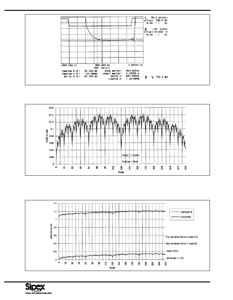
(X) Current versus Code.
V
DD
= 5V
V
IN
= 0.05V to 1.55V
V
OUT
= 0.1V to 3.1V
Plot 12. I
REFL
Current Input Current versus Code.

274
Plot 13. Typical Midscale Output versus Temperature.
Plot 14. Supply Current versus Temperature.
Plot 15. Output Short Circuit Current versus V
OUT
(X).

275
Plot 16. Sink Current at Zero Scale.
Plot 17. Typical V
OUT
max versus V
DD
.
Plot 18. Typical V
OUT
min versus V
DD
versus I
SINK
.

276
Plot 20. Integral Error versus Code versus V
DD
; V
IN
(X) = 0.6V.
Plot 19. Integral Error versus Code versus V
DD
; V
IN
(X) = 0.5V.

277
a)
b)
c)
d)
Plot 21. Pulse Response -- a) C
LOAD
= 470pF, R
LOAD
= 10MOhm; b) C
LOAD
= 470pF, R
LOAD
= 1kOhm; c) 50Ohms in series
with C
LOAD
= 470pF; d) R
LOAD
= 1kOhm, 50Ohms in series with C
LOAD
= 470pF.

278
a)
b)
c)
d)
Plot 22. Pulse Response -- a) C
LOAD
= 4,700pF; b) C
LOAD
= 4,700pF, R
LOAD
= 1kOhm; c) 30 Ohms in series with C
LOAD
=
4,700pF; d) R
LOAD
= 1kOhm, 30Ohms in series with C
LOAD
= 4,700pF.

279
a)
b)
c)
d)
Plot 23. Pulse Response -- a) C
LOAD
= 47,000pF; b) C
LOAD
= 47,000pF, R
LOAD
= 1kOhm; c) 15 Ohms in series with C
LOAD
=
47,000pF; d) R
LOAD
= 1kOhm, 15 Ohms in series with C
LOAD
= 47,000pF.

280
a)
b)
c)
d)
Plot 24. Pulse Response -- a) C
LOAD
= 0.47
µ
F; b) C
LOAD
= 0.47
µ
F, R
LOAD
= 1kOhm; c) 8.2 Ohms in series with C
LOAD
=
0.47
µ
F; d) R
LOAD
= 1kOhm, 8.2 Ohms in series with C
LOAD
= 0.47
µ
F.

281
PINOUT
24 V
OUT
D
23 V
IN
C
22 V
IN
D
21 V
DD
20 SDI
19 GND
18 SDO
17 CLOCK
16 LOADH
15 V
IN
H
14 V
IN
G
13 V
OUT
H
V
OUT
C 1
V
OUT
B 2
V
OUT
A 3
V
IN
B 4
V
IN
A 5
V
REFL
6
PRESETL 7
V
IN
E 8
V
IN
F 9
V
OUT
E 10
V
OUT
F 11
V
OUT
G 12
SP9841
20 V
OUT
D
19 V
IN
C/D
18 V
DD
17 SDI
16 GND
15 SDO
14 CLOCK
13 LOADH
12 V
IN
G/H
11 V
OUT
H
V
OUT
C 1
V
OUT
B 2
V
OUT
A 3
V
IN
A/B 4
V
REF
L 5
PRESETL 6
V
IN
E/F 7
V
OUT
E 8
V
OUT
F 9
V
OUT
G 10
SP9842
Pin 18 -- SDO -- Serial Data Output; active totem≠
pole output.
Pin 19 -- GND -- Ground.
Pin 20 -- SDI -- Serial Data Input.
Pin 21 -- V
DD
-- Positive 5V Power Supply.
Pin 22 -- V
IN
D -- DAC D Reference Voltage Input.
Pin 23 -- V
IN
C -- DAC C Reference Voltage Input.
Pin 24 -- V
OUT
D -- DAC D Voltage Output.
SP9842 PINOUT
Pin 1 -- V
OUT
C -- DAC C Voltage Output.
Pin 2 -- V
OUT
B -- DAC B Voltage Output.
Pin 3 -- V
OUT
A -- DAC A Voltage Output.
Pin 4 -- V
IN
A/B -- DAC A and B Reference Voltage
Input.
Pin 5 -- V
REF
L -- DAC Reference Voltage Input
Low, common to all DACs.
Pin 6 -- PRESETL -- Preset Input; active low; all
DAC registers forced to 80
H
.
Pin 7 -- V
IN
E/F -- DAC E and F Reference Voltage
Input.
Pin 8 -- V
OUT
E -- DAC E Voltage Output.
Pin 9 -- V
OUT
F -- DAC F Voltage Output.
SP9841 PINOUT
Pin 1 -- V
OUT
C -- DAC C Voltage Output.
Pin 2 -- V
OUT
B -- DAC B Voltage Output.
Pin 3 -- V
OUT
A -- DAC A Voltage Output.
Pin 4 -- V
IN
B -- DAC B Reference Voltage Input.
Pin 5 -- V
IN
A -- DAC A Reference Voltage Input.
Pin 6 -- V
REF
L -- DAC Reference Voltage Input
Low, common to all DACs.
Pin 7 -- PRESETL -- Preset Input; active low; all
DAC registers forced to 80
H
.
Pin 8 -- V
IN
E -- DAC E Reference Voltage Input.
Pin 9 -- V
IN
F -- DAC F Reference Voltage Input.
Pin 10 -- V
OUT
E -- DAC E Voltage Output.
Pin 11 -- V
OUT
F -- DAC F Voltage Output.
Pin 12 -- V
OUT
G -- DAC G Voltage Output.
Pin 13 -- V
OUT
H -- DAC H Voltage Output.
Pin 14 -- V
IN
G -- DAC G Reference Voltage Input.
Pin 15 -- V
IN
H -- DAC H Reference Voltage Input.
Pin 16 -- LOADH -- Load DAC Register Strobe;
active high input that transfers the data bits from the
Serial Input Register into the decoded DAC Register.
Refer to Table 1.
Pin 17 -- CLOCK -- Serial Clock Input; positive≠
edge triggered.

282
Pin 10 -- V
OUT
G -- DACG Voltage Output.
Pin 11 -- V
OUT
H -- DACH Voltage Output.
Pin 12 -- V
IN
G/H -- DACG and H Reference
Voltage Input.
Pin 13 -- LOADH -- Load DAC Register Strobe;
active high input that transfers the data bits from the
Serial Input Register into the decoded DAC Register.
Refer to Table 1.
Pin 14 -- CLOCK -- Serial Clock Input; positive≠
edge triggered.
Pin 15 -- SDO -- Serial Data Output; active totem≠
pole output.
Pin 16 -- GND -- Ground.
Pin 17 -- SDI -- Serial Data Input.
Pin 18 -- V
DD
-- Positive 5V Power Supply.
Pin 19 -- V
IN
C/D -- DACC and D Reference
Voltage Input.
Pin 20 -- V
OUT
D -- DACD Voltage Output.
FEATURES...
The SP9841 and SP9842 include eight separate op
amp≠buffered eight≠bit DACs. These can be used to
replace up to eight trimpots with eight low≠imped-
ance programmable sources. The SP9841 uses eight
separate multiplying reference inputs, while the
SP9842 provides four pair of multiplying inputs. All
of the reference inputs, in either case, are returned to
a common voltage reference low pin. The inherent 2X
gain from the two≠quadrant multiplying reference
inputs to the outputs allows the use of AC or DC
multiplying reference inputs generated from a single,
low supply voltage.
Each DAC has its own data register which holds its
output state. These data registers are updated from an
internal serial-to-parallel shift register which is loaded
from a standard 3-wire serial input digital interface.
Twelve data bits make up the data word clocked into
the serial input register. This data word is decoded
such that the first 4 bits determine the address of the
DAC register to be loaded and the last 8 bits are the
data. A serial data output pin at the opposite end of the
serial register allows simple daisy-chaining in mul-
Table 1. Serial Input Decoded Truth Table
LAST
D
0
LSB
DATA ADDRESS
D
1
D
2
D
3
D
4
D
5
D
6
D
7
MSB
D
7
D
6
D
5
D
4
D
3
D
2
D
1
D
0
DAC Output Voltage
V
OUT
= D/128 (V
IN
≠ V
REF
L) + V
REF
L
V
REF
L
1/128 (V
IN
≠ V
REF
L) + V
REF
L
127/128 (V
IN
≠ V
REF
L) + V
REF
L
V
IN
(Preset Value)
129/128 (V
IN
≠ V
REF
L) + V
REF
L
254/128 (V
IN
≠ V
REF
L) + V
REF
L
255/128 (V
IN
≠ V
REF
L) + V
REF
L
A
0
LSB
A
1
A
2
A
3
MSB
A
3
A
2
A
1
A
0
DAC Updated
FIRST
0
0
0
0
0
0
0
0
1
1
.
.
1
0
0
0
1
1
1
1
0
0
1
0
0
1
1
0
0
1
0
0
1
1
0
0
1
0
0
1
1
0
0
1
0
0
.
.
.
1
1
0
0
1
0
0
1
1
0
0
1
0
0
1
1
0
1
1
0
1
0
1
0
0
0
0
1
1
1
1
0
0
.
.
1
0
0
1
1
0
0
1
1
0
0
.
.
1
0
1
0
1
0
1
0
1
0
1
.
.
1
No Operation
DACA
DACB
DACC
DACD
DACE
DACF
DACG
DACH
No Operation
.
.
No operation
.
.
.
.
.
.
.
.
.

283
tiple DAC applications without additional external
decoding logic.
The SP9841/9842 consume only 65 mW from a
single +5V power supply. The SP9841 is available in
24-pin plastic DIP and SOIC packages. The SP9842
is available in a space≠saving 20≠pin SOIC package.
For applications requiring code≠controlled output
polarity reversal regardless of the reference input level
(i.e. four≠quadrant multiplication), please see the
SP9840/SP9843 product data sheet.
USING THE SP9841/9842
Theory of Operation
Each of the eight channels of the SP9841/SP9842 can
be used for signal reconstruction, as a programmable
dc source, or as a programmable gain/attenuation
block, multiplying an ac reference input by factors of
0 to 1.992. The rugged, wideband output amplifiers
provide both current sink and source capability for dc
applications, even those driving difficult loads. The dc
source mode mimics the functionality of a program-
mable trimpot with the added benefit of a low imped-
ance buffered output. The amplifier's bandwidth and
high open≠loop gain allow its use in programmable
gain applications where even a low distortion, high
resolution signal (such as audio) must be gated on and
off or gain≠controlled over a ≠42 to +6dB range.
Each channel consists of a voltage≠output DAC,
implemented using CMOS switches and thin≠film
resistors in a inverted R≠2R ladder configuration.
Each DAC drives the positive terminal of an op amp
+
≠
8
DAC 1
R
R
V
IN
V
DAC
V
OUT
V
OUT
= 2 X V
DAC
when V
REF
L = 0V
= 2(D/256) X V
IN
= D/128 X V
IN
V
REF
L
V
OUT
= D/128 X (V
IN
≠ V
REF
L) +V
REF
L
Figure 1. DAC and Output Amplifier Circuit
configured for a non≠inverting gain of 2 using equal
value thin≠film feedback and gain≠setting resistors.
Signal ground is the V
REFL
pin, the common reference
input return for the 8 DAC≠op amp channels. As
shown in Figure 1, the DAC section can be thought of
as a potentiometer across V
IN
(X) to V
REFL
. When this
potentiometer reaches its maximum output value of
255/256 times V
IN
, the output will be 1+(R
FB
/R
GAIN
) or
2 times the value of V
DAC
(actually up to 1.9921875
times the input voltage, with V
REFL
tied to ground).
When the potentiometer is at its minimum value of 0/
256, the output will try to be 0V, again assuming V
REFL
is tied to ground.
The true relation between the dc levels at the V
IN
pin,
V
REFL
and the output can be described as:
V
OUT
= ((1 + R
FB
/R
G
) * (Data/256) * (V
IN
≠ V
REFL
)) + V
REFL
where Data is programmable from 0 to 255, and R
FB
= R
G
.
2.5
1.5
0
V
OUT(X)
(Volts)
0
0.5
1.5
V
REF
L= 0V
V
IN(X)
(Volts)
D = FF
H
D = 80
H
D = 00
H
1.0
0.5
1.0
2.0
3.0
2.5
1.5
0
V
OUT(X)
(Volts)
0.75
2.25
V
REF
L= 1.5V
V
IN(X)
(Volts)
D = FF
H
D = 80
H
D = 00
H
1.5
0.5
1.0
2.0
3.0
Figure 2. a) Single≠Quadrant, and b) Two≠Quadrant Operation
a)
b)

284
When V
REFL
is tied to ground, this expression
reduces to:
V
OUT
= (Data/128) *V
IN
Multiplication of Input Voltages
While both the SP9841 and SP9842 are capable of
two≠quadrant multiplication, this terminology is not
very precise when describing a system which runs
from a single positive supply. Traditionally, the quad-
rants have been defined with respect to 0V. A two≠
quadrant multiplying DAC could produce negative
output voltages only if a negative voltage reference
were applied. A four≠quadrant device could also
produce a code≠controlled negative output from a
positive reference, or a code≠controlled positive out-
put from a negative reference. If ground is used to
delineate the quadrants, then the SP9841/SP9842
should be considered single≠quadrant multiplying
devices, as their output op amps cannot produce
voltages below ground.
In reality, it is possible to define a dc voltage as a signal
ground in a single supply system. If the DAC's V
REFL
pin is driven to the voltage chosen as pseudoground,
then each voltage output will exhibit 2≠quadrant
behavior with respect to pseudoground; that is the
output voltage will enter the quadrant below the
pseudoground only when the reference input voltage
goes below pseudoground. This mode of operation is
useful when implementing programmable gain/at-
tenuator sections, especially when the input signal is
bipolar with respect to pseudoground, or is ac≠
coupled into the V
IN
(X) pin. When V
REFL
is tied to
power supply ground, only output voltages greater
than V
REFL
are possible, and the device performs
single≠quadrant multiplication, much like a buffered
programmable trimpot across a single supply. Fig-
ures 2a and 2b show single≠quadrant and 2≠quadrant
performance of the SP9841/SP9842. Applications
which require 4≠quadrant operation with respect to
pseudoground should use the SIPEX SP9840 or
SP9843 4≠quadrant multiplying DACs.
The choice of voltage to use for the pseudoground is
limited by the legal voltage swing at the op amp
output. The op amp exhibits excellent linearity for
output voltages between, conservatively, 100mV and
V
DD
≠ 1.5V. The op amp BiCMOS output stage
consists of an npn follower loaded by an NMOS
common sourced to ground. This circuit exhibits
wide bandwidth and can source large currents, while
retaining the capability of driving the output to volt-
ages close to ground.
At output voltages below 25mV, feedback forces
some op amp internal nodes toward the supply rails.
The NMOS pull≠down device gets driven hard and
the NMOS device enters the linear range -- it begins
to function in the same manner as a 50 ohm resistor.
In reality, the wideband amplifier output stage sinks
some internal quiescent current even when driving the
output towards ground. This sunk current drops
across the output stage NMOS transistor ON≠resis-
tance and internal routing resistance to provide a
minimum output voltage, below which the amplifier
cannot drive. This minimum voltage is in the 15
to 25mV range. It varies within a package with
each op amp's offset voltage and biasing varia-
tions. If an input voltage lower than this mini-
mum, such as code 0 or 1, when V
REFL
is ground,
2.5
1.5
0
V
IN(X)
(Volts)
V
REFL
(Volts)
0.5
1.0
2.0
3.0
0
0.5
1.0
1.5
2.0
2.5
3.0
V
DD
= 4.75V minimum; V
OUTMAX
< +3.25V
2.5
1.5
0
V
IN(X)
(Volts)
V
REFL
(Volts)
0.5
1.0
2.0
3.0
0
0.5
1.0
1.5
2.0
2.5
3.0
V
DD
= 4.75V minimum; V
OUTMAX
>100mV
a)
b)
Figure 3. Reference Voltages a) Normal Operation; b) Maximum Linearity Near Code 1

285
is requested, feedback within the op amp circuit
will force internal nodes to the rails, while the
output will remain saturated near this minimum
value. Non≠saturated monotonic behavior returns
between 25mV and 100mV at the output, but full
open loop gain and linearity are not apparent until
the output voltage is nearly 100mV above the
negative supply. Applications which require good
linearity for codes near zero should drive the V
REFL
input at least 100mV above the ground pin, as this
insures that the output voltage will not go below
100mV for any legal input voltage. Two≠quadrant
applications (programmable gain/attenuator) usually
bias V
REFL
up at system pseudoground, well above this
saturation region, and therefore maintain linearity
even at high attenuations (i.e. at code 1).
The allowable, useful values of V
IN
(X) and V
REFL
are
limited if a legal output value is to be expected for all
input codes. At maximum gain (DAC code 255) V
OUT
is approximately equal to 2V
IN
(X) ≠ V
REFL
. By solving
this equation twice, once with V
OUT
set to 0V, and then
again with Vout set to V
DD
≠1.5V, the chart of Figure
3a results. This chart can be used to find the maximal
V
IN
(X) voltage excursions for any given voltage
driven into V
REFL
. The upper line plots the maximum
voltage at V
IN
(X) and the lower line plots the mini-
mum voltage at V
IN
(X) at each value of V
REFL
drive.
Normal operation would be for V
IN
(X) anywhere
between the two lines. For example, assume a 4.75V
supply voltage, and that the DAC code is set to 255. If
V
REFL
is driven to 1.6V, V
IN
(X) below 0.8V would
require the output amplifier to swing below ground.
V
IN
(X) above 2.425V would require output voltages
greater than V
DD
≠ 1.5V, or 3.25V.
Figure 3b shows the limits on V
IN
when the mini-
mum V
OUT
is constrained to be greater than 100mV,
for extremely linear operation, even at DAC code
1. In this case, the lower line is 50mV above its
position in Figure 3a, except that below V
REFL
=
100mV, the minimum input voltage stays at
100mV. It should be noted that V
IN
(X) can always
be driven to or slightly beyond the supply rails
without harm. Under such circumstances, the DAC
code can always be set to provide sufficient attenu-
ation to get an undistorted output.
Driving the Reference Inputs
The V
IN
inputs exhibit a code≠dependent input resis-
tance, as shown in the specifications. In general, these
inputs should be driven by an amplifier capable of
handling the specified load resistance and capaci-
tance. The reference inputs are useful for both ac and
dc input sources. However, series resistance into these
pins will degrade the linearity of the DAC. A series
resistance of 50 Ohms can cause up to 0.5LSB of
additional integral linearity degradation for codes
near full scale, due to the code≠dependent input
current dropping across this error resistance. AC≠
coupled applications should use the largest capacitor
value (lowest series resistance) which is practical, or,
use an external buffer to drive the inputs.
The DAC switches function in a break≠before≠make
manner in order to minimize current spikes at the
reference inputs. As previously noted, the reference
inputs can withstand driving voltages slightly beyond
the power supply rails without harm. The gain of 2 at
the op amps limits the choice of V
IN
/V
REFL
combina-
tions if clipping is to be avoided at the higher codes.
Output Considerations
Each DAC output amplifier can easily drive 1Kohm
loads in parallel with 15pF at its rated slew rate. The
unique BiCMOS amplifier design also ensures stabil-
ity into heavily capacitive loads -- up to 47,000pF.
Under these conditions, the slew rate will be limited by
the instantaneous current available for charging the
capacitance -- the slew rate will be severely degraded,
and some damped ringing will occur. Especially
under heavy capacitive loading, a large, low imped-
ance local bypass capacitor will be required. A
0.047
µ
F ceramic in parallel with a low≠ESR 2.2 to
10
µ
F tantalum are recommended for worst≠case loads.
The amplifier outputs can withstand momentary
shorts to V
DD
or ground. Continuous short circuit
operation can result in thermally induced damage,
and should be avoided.
If the input reference voltage is reduced to 0.6V, then
both the amplifier and DAC are functional at room
temperature at supply voltages as low as 2.5V. At V
DD
= 2.7V, power dissipation is 9.3mW typical, with the
serial clock at 4MHz, or 7.0mW typical with the serial
clock gated off.
Interfacing to the SP9841/SP9842
A simple serial interface, similar to that used in a
74HC594 shift≠register with output latch, has been
implemented in these products. A serial clock is used

286
Figure 4. Timing.
CHARACTERISTICS
(Typical @ 25
∞
C with V
DD
= +5V unless otherwise noted.)
PARAMETER
MIN.
TYP.
MAX.
UNIT
CONDITIONS
Input Clock Pulse Width (t
CH
, t
CL
)
50
ns
Data Setup Time (t
DS
)
30
ns
Data Hold Time (t
DH
)
20
ns
CLK to SDO Propagation Delay (t
PD
)
100
ns
DAC Register Load Pulse Width (t
LD
)
50
ns
Preset Pulse Width (t
PR
)
50
ns
Clock Edge to Load Time (t
CKLD
)
30
ns
Load Edge to Next Clock Edge(t
LDCK
)
60
ns
1
0
A
3
A
2
A
1
A
0
D
7
D
6
D
5
D
4
D
3
D
2
D
1
D
0
1
0
1
0
FS
0
SDI
CLOCK
LOAD
V
OUT
1
0
1
0
1
0
(FF
H
)
(08
H
)
SERIAL
DATA IN
SERIAL DATA INPUT TIMING DETAIL (PRESET = Logic "1"; V
IN(X)
= 1.5V; V
REF
L = 0V)
1
0
SERIAL
DATA OUT
CLOCK
LOAD
V
OUT
t
DS
t
CH
t
CL
t
LD
t
S
t
LDCK
±1 LSB
ERROR BAND
t
CLKD
t
PD
t
DH
A
X
or
D
X
1
0
PRESET
t
S
t
PR
±1 LSB
ERROR BAND
(FF
H
)
(08
H
)
V
OUT
Table 2. Logic Control Input Truth Table.
SDI
CLK
LOADH
PRESETL
LOGIC OPERATION
X
L
L
H
No Change
Data
L
H
Shift In One Bit from SDI
Shift Out 12≠clock delayed data at SDO
X
X
X
L
All DAC Registers Preset to 80
H
(Note 1)
X
L
H
H
Load Serial Register Data into DAC(X) Register
Note 1: "Preset" may not persist at all DACs if LOADH is high when PRESETL returns high.

287
to strobe serial data into a 12≠stage shift≠register at
each rising clock edge. The first four serial bits contain
the address of the DAC to be updated, MSB first. The
next 8 bits contain the binary value to be loaded into
the desired DAC, again MSB first. After the 12th serial
bit is clocked in, the LOADH line can be strobed to
latch the 8 bits of data into the data holding register for
the desired DAC. The address bits feed a decoding
network which steers the LOADH pulse to the clock
input of the desired DAC data holding register. The
output of the 12th shift≠register is also buffered and
brought out as the SERIAL DATA OUT (SDO),
which can be used to cascade multiple devices, or for
data verification purposes.
The address field is set up such that DAC A is
addressed at 0001 (binary). Address 0000(binary)
will not affect the operation of any channel, as this
combination is easily generated inadvertently at
power≠up. Other no≠operation addresses exist at
1001(binary) through 1111(binary). Another use for
no≠operation addresses is to mask off updates of any
DAC channel in a multiple≠part system with cas-
caded serial inputs and outputs. By sending a valid
address and data only to the desired channel, it is
possible to simplify the system hardware by driving
the LOADH pin at each part in parallel from a single
source. Table 1 shows a register≠level diagram of the
addresses, data, and the resulting operation.
A fourth control pin, PRESETL, can be used to
simultaneously preset all DAC data holding registers
to their mid≠scale (80
H
) values. This will asynchro-
nously force all DAC outputs to buffer the voltages at
their respective inputs to their outputs with unity gain.
This feature is useful at power≠up, as a simple resistor
to the supply and capacitor to ground can insure that
all DAC outputs start at a known voltage. It can also
be used to implement stand-alone (non≠programmed)
applications, such as a unity gain octal cable driver.
Table 2 summarizes the operation of the four digital
control inputs.
The four digital control input pins have been
designed to accept TTL (0.8V to 2.0V minimum)
or full 5V CMOS input levels. Timing information
is shown in Figure 4. Serial data is fully clocked
into the shift≠register after 12 clock rising edges,
subject to the described setup and hold times. After
the shift≠register data is valid, the LOADH line
can be pulsed high to load data into the desired
DAC data register, which switches the DAC to the
new input code. The serial clock input should not
see a rising edge while the LOADH pulse is high
in order to prevent shift≠register data from corrup-
tion during data register loading.
The serial clock and data input pins are designed to be
compatible as slaves under National Semiconductor's
MicrowireTM and MicrowirePlusTM protocols and
under Motorola's SPITM and QSPITM protocols. In
some micro≠controllers, the interface is completed by
programming a bit in a general≠purpose I/O port as a
level, used to strobe the LOADH line at the DACs.
This is done in a manner similar to that used for
generating a CS signal, which is necessary when
driving some other MicrowireTM peripherals.
Low Voltage Operation
At nominal V
DD
, the CMOS switches used in the
DAC obtain sufficient drive to maintain an ON-
resistance much lower than the thin≠film resistors.
This keeps the non≠linear voltage≠dependent portion
of their ON-resistances low, and guarantees both
excellent DAC linearity versus code, and low≠distor-
tion multiplication of large≠swinging AC inputs. The
devices in the op amp also receive sufficient drive to
guarantee the specified bandwidth and output drive
current. However, all circuits within the DACs are
quite "functional" at very low values of V
DD
. By
reducing the reference voltages such that the maxi-
mum V
OUT
is near the target of V
DD
-1.5V, the DACs
will provide better than 0.5LSB typical integral per-
formance for DC output voltages between 100mV
and V
DD
-1.5V. Reducing the reference voltage actu-
ally aids the linearity of the DACs, even at nominal
V
DD
. This occurs because the NMOS half of the
CMOS switches are more fully utilized at reference
voltages closer to ground, thus further reducing the
ON≠resistance of the switches. Reference input cur-
rents are proportional to the reference voltages and
will also decrease with the reference voltages.
Plot 19 shows typical DC output linearity for V
IN
(X)
set to 0.5V, with V
DD
at 2.5, and then 3.5V. Note that
at 3.5V, the linearity is actually much better than the
±
0.25LSB typical performance at V
IN
(X) = 1.625V
and V
DD
= 5V. Similarly, Plot 20 shows that this
performance level persists for V
DD
= 4.5V and 5.5V,
with V
IN
(X) set to 0.6V. The price paid for low voltage
operation is in op amp gain, bandwidth and es≠
pecially current sinking at the DAC output. Plots 17

288
through 19 show that for lower output current values
less than 1 mA, the SP9841/9842 can be used effec-
tively even with V
DD
in the range of 2.7 to 3.3V.
Application Circuits
Figure 5 shows an inexpensive single≠quadrant
DC source for generating voltages from near
ground to near 2.44V. When using a two≠termi-
nal reference, the pull≠up resistor should be
chosen so that the minimum input resistance of
5kOhms at each V
IN
(X) can be driven at the
lowest expected V
DD
. At V
DD
= 4.75V, and V
REFL
= 1.25V, each input to be driven needs 0.248mA,
and the regulator needs 0.1mA to stay well
regulated. Thus, to drive all eight inputs, R
PULLUP
should be chosen to supply at least 2mA. To
operate at 4.75V, 1.75kOhms is required; the
1.5kOhms shown will suffice even if its value is
5% high. To drive a single input, a 10kOhm
value could be used. In order to reduce reference
and supply generated noise, an optional capaci-
tor of 1 to 100
µ
F bypasses the reference.
Figure 6 shows a circuit which generates DC
voltages roughly symmetric with respect to
2.446V. Two bandgap references are stacked to
first drive V
REFL
to 1.223V, and the input to 2.446V.
The pull≠up resistor value should again be scaled
for worst≠case loading -- in order to drive all eight
inputs at 4.75V, a value of 620 Ohms is required.
At fullscale, the DAC output is near 3.65V. While
typical units will source 5mA at an output voltage
Figure 5. Inexpensive DC Source.
+
≠
DC
OUT
1/8 of SP9841
3
+5V
1.22V
DC
OUT
= 20mV to +2.44V for DATA = 00
H
to FF
H
.
At PRESET, DC
OUT
= +1.22V
R
PULLUP
1.5kOhms
ICL8069
45µF*
(*Optional Noise Reduction)
Figure 6. Pseudo Bipolar Source Generates Voltages Above and Below 2.44V.
+
≠
DC
OUT
1/8 of SP9841
3
+5V
1.22V
DC
OUT
= +1.22V to +3.66V for DATA = 00
H
to FF
H
.
At PRESET, DC
OUT
= +2.44V
2kOhm
ICL8069
1.22V
ICL8069
+1.22V
+2.44V
45µF*
(*Optional Noise Reduction)
45µF*

289
Figure 7. Generating Programmable DC Voltages.
+
≠
DC
OUT
1/8 of SP9841
3
ICL8069
+
≠
OP≠90
1.22V
R1
10K
R2
4.75K
+1.8V
DC
OUT
= 20mV to +3.6V for DATA = 00
H
to FF
H
.
At PRESET, DC
OUT
= +1.8V
+ ≠
R3
1.2K
45µF*
(*Optional Noise Reduction)
V
I
Figure 8 shows a non≠programmed standalone appli-
cation. By tying PRESETL to ground, all channels are
permanently set to unity gain. While preset, the input
impedance at each input is set to 40kOhms nominal
(20kOhms minimum), which minimizes required
input current drive. The TL431 reference is pro-
grammed by resistors R
1
and R
2
for 3.3V. R
3
is chosen
to provide at least 165
µ
A for each input driven, plus
0.5mA for the reference at the minimum supply value
to be considered. In the Figure, the 560 Ohms shown
will drive all eight inputs. The excellent capacitive
load capability of the output amplifiers handles any
value of capacitive bypass loads without oscillation;
however, to minimize ringing at powerup, load ca-
pacitance can be chosen to be greater than 0.1
µ
F or
less than 1,000pF.
of 3.75V while running from a 4.75V supply, this
behavior is not tested in device production. If
maximum linearity is required near the 3.66V
fullscale voltage, then output loading should be
kept under 1mA.
Figure 7 uses a 1.8V reference to provide an output
voltage range from near ground to almost 3.6V.
The external micropower reference uses a bandgap
in a bootstrapped configuration, which guarantees
excellent supply rejection. Voltage at V
1
is set by
1.223
R2
(R1
R2)
+
V
OUT
is 1.223V +V
1
. R
3
is used to set the quies-
cent current through the bandgap, I=V
1
/R
3
. The
op amp will easily drive one to all eight inputs.
Figure 8. Generating Up to Eight (8) 3.3V @ 10mA DC Supplies with Logic≠Level Controlled Shutdown (Non≠Programmed).
+
≠
DC
OUT
1/8 of SP9841
PRESET
Eight independent 3.3V @ 10mA supplies with
logic≠level controlled shutdown.
32K
+5V
+
≠
2.5V
100K
TL431
560
AC04
DIG
IN
DIG
IN
DC
OUT
0
1
3.3V
0V

290
Figure 9 shows a DAC channel controlling the output
voltage of an LM317 voltage regulator. By program-
ming the code, the DAC changes its own supply
voltage. This circuit can be modified for wider output
voltage ranges by reducing the value of R
4
. However,
the circuit as shown requires the DAC to sink 1mA to
the negative rail at code 0 at its lowest V
DD
, at which
point the output voltage is 62mV. Thus, programming
codes 0 through 5 will do little to influence the output.
If R
4
is replaced with a short circuit, useful operation
would be between 3.9V and 6.15V output; however,
the DAC output must then sink 2.5mA at V
DD
= 3.9V,
which results in a minimum DAC output voltage of
Figure 9. Programmable 1Amp Power Source.
+
≠
V
OUT
1/8 of SP9841
3
+12V
ICL8069
At PRESET, V
OUT
= 5.0V
10kOhms
R1
499Ohms
V
A
V
OUT
= 4.5V TO 5.5V at 1Amp for DATA = 00
H
to FF
H
.
LM317
10µF
In Out
Adjust
R2
1kOhms
R3
511Ohms
1.22V
V
DD
R4
681Ohms
around 150mV. Codes above 17 will then provide
equally spaced output voltage increments.
Figure 10 shows how the gain of an external non≠
inverting op amp can be programmed. R
F
and R
G
are
chosen for nominal gain. R
TRIMRANGE
is then ratioed to
R
F
to provide the desired range of gain trim. A wide
gain grange is achievable -- for example, with R
F
=
11kOhms, R
G
= 1kOhms and R
TRIMRANGE
= 2.74kOhms,
gain would be programmed linearly from 8 to just
under 16.
The OP≠491 shown in Figure 10 is capable for
Figure 10. Adjustable Gain of External Non≠Inverting Opamp Circuit; V
OUT
= Rail≠to≠rail.
+
≠
SIG OUT
1/8 of SP9841
3
1/4 of OP≠491
+5V
Set R
TRIMRANGE
for desired gain-trim range.
For R
TRIMRANGE
= 20kOhms:
Code 0, A
V
= +5.5
Code 128, A
V
= +5.0
Code 255, A
V
= +4.51
+
≠
R
F
10kOhms
R
TRIMRANGE
20kOhms
R
IBIAS
50kOhms
V
REFL
= Up to V
DD
/2
(2.5V nominal for
rail≠to≠rail output
at SIG OUT)
1V
P-P
2.2µF
R
GAIN
2.5kOhms
V
REFL
A
R
R
V
F
G
F
TRIMRANGE
D
R
R
= +
+
-
1
1
128
, D = 0 to 255
+5V
V
DD

291
rail≠to≠rail output swing. In order to obtain this
performance, V
REFL
must be externally driven to
V
DD
/2, perhaps by use of the circuit of Figure 11.
At V
REFL
near 2.5V and V
DD
= 4.75V, the typical
positive output headroom at the DAC is limited
to 1.15V above 2.5V, so that this circuit is useful
for rail≠to≠rail outputs for gains higher than
4.35 (i.e. 1.15V
PP
maximum input). Note that
while an AC≠coupled input is shown, this cir-
cuit is just as useful for DC≠coupled inputs
which are generated with respect to the V
REFL
pseudoground voltage. R
IBIAS
is used for the
AC≠coupled circuit for opamp bias current re-
turn when the DAC is programmed to code 0, as
no current flows into V
IN
(X) at code 0.
Figure 11 shows a minimal parts count method
Figure 11. Programmable, Bootstrapped, 1.4V to 2.2V V
REFL
Drive.
The usable range for the bootstrapped V
REFL
circuit is 1.4 to 2.4V
OUT
at V
DD
= 5V, R
ISRC
= 2kOhms.
To increase the upper usable limit, decrease value of R
ISRC
.
+
≠
V
OUT
A
1/8 of SP9841
3
ICL8069
At PRESET, V
OUT
= 1.3V
(not well≠regulated)
R
ISRC
2kOhm
Load code
45µF*
301Ohm
1.22V
+ ≠
V
REFL
V
IN
A
+
≠
1/8 of SP9841
3
V
IN
B
*(Optional Noise Reduction)
+5V
112 for 1.4V
OUT
= V
REFL
96 for 1.6V
OUT
= V
REFL
70 for 2.2V
OUT
= V
REFL
V
OUT
B
+
≠
1/8 of SP9841
3
V
IN
H
V
OUT
H

292
of generating a programmable pseudoground
voltage at the V
REFL
terminal. A pseudoground is
very useful if any channels are to be used in AC≠
multiplying applications. In such applications,
the pseudoground will set the DC offset of the
output signal. The voltage output of this circuit
as the code is decreased is non≠linear because
the DAC bootstraps the increased output volt-
age by a larger fraction at each code. It is really
meant to be programmed only over a range of
codes between 104 and perhaps 60. It does
exhibit a fairly well≠defined output, even if
non≠intentional codes are programmed. For
codes above 112, the output stage resembles a
50 Ohm resistor to ground, and the V
REFL
output
will be near 1.3V, depending upon the loading at
the other V
IN
(X) inputs. For codes below 60, the
output voltage will continue to rise until limited
by available current through R
ISRC
. Note that
R
ISRC
supplies the actual current into V
REFL
, and
must be chosen in order to supply enough cur-
rent for all channels, especially if any of the
other eight inputs are to be grounded. A plot of
V
REFL
versus code is shown with the Figure, for
all other inputs either grounded or tied to the
supply.
Figure 12 shows a programmable gain/attenua-
tor section using the programmable VREFL
drive. The VREFL of each DAC is actually
internally connected. When the optional 45
µ
F
noise reduction capacitor is included, this cir-
cuit is capable of 86dB of SNR and 74 to 84dB
of SINAD at 1kHz, depending on the pro-
Figure 12. AC≠Coupled, Programmable Gain/Attenuator with Bootstrapped Programmable Output DC Offset (V
REFL
Drive).
+
≠
V
OUT
A
1/8 of SP9841
3
ICL8069
R
ISRC
2kOhm
Load DACA with code 90; sets V
REFL
=1.7V.
Then, load DACB with desired gain:
45µF*
301
1.22V
+ ≠
V
REFL
V
IN
A
*(Optional Noise Reduction)
+5V
code 255 = +6dB
code 128 = 0dB
code 64 = ≠6dB
code 1 = ≠42dB
code 0 = ≠70dB
+
≠
V
OUT
B
1/8 of SP9841
V
REFL
V
IN
B
2.2µF
±0.75V

293
grammed gain. Please refer to the THD versus
Frequency plot, which was generated by termi-
nating a 600 Ohm source with 150 Ohms to
ground, then into this circuit. For the best gain
linearity versus code, use the largest (lowest
series impedance) coupling capacitor available,
or externally buffer the input.
Figure 13 shows an external op amp with an
inverting programmable gain. In this circuit the
maximum output swing at the DAC occurs at the
maximum circuit gain. Thus, the headroom re-
striction at the DAC output applies at the maxi-
mum gain, which, for rail≠to≠rail outputs (V
REFL
= 2.5V or V
DD
/2) should be greater than 4.3. By
making the programmable gain range large, this
circuit can be used to provide rail≠to≠rail out-
puts even at the lower gains. This circuit has
been ratioed to provide exact integer gain incre-
ments for every increase in 25 codes, over the
range of ≠1 to ≠11. This large range of gain
comes at a slight cost -- the output offset of the
DAC amplifier will be gained up by ≠5.12 times
at SIG OUT. If this is a problem, a second DAC
channel can be set up with a programmable DC
offset adjustment with its output summed through
a large resistor into the OP≠491 inverting termi-
nal. Note that when RTRIMRANGE is set up for
only unity gain change range as in Figure 12,
only ≠0.5 times the DAC output offset will
appear at SIG OUT.
Another application for the circuits of both
Figure 10 and 13 could be to force precise gains
from circuits made from imprecise resistors. By
restricting the programmable gain range to
±
2%
(by setting R
TRIMRANGE
to be 100 times R
F
), the
resistors could be 1% values and the program-
mable gain resolution would increase to better
than 12≠bits (0.0156%). In this case, only 1% of
the DAC output offset voltage would appear at
SIG OUT.
Figure 14 shows a window comparator and two
channels of programmable-gain input. While
the input signal is shown as AC≠coupled, DC
signals of up to rail≠to≠rail amplitude could be
measured by setting the attenuation at the signal
Figure 13. Adjustable Gain of External Inverting Opamp Circuit, V
OUT
= Rail≠to≠Rail.
+
≠
SIG OUT
1/8 of SP9841
3
1/4 of OP≠491
+5V
Set R
TRIMRANGE
for desired gain-trim range.
For R
TRIMRANGE
= 1.5kOhms:
Code 0, A
V
= -1
Code 25, A
V
= -2
Code 75, A
V
= -4
Code 175, A
V
= -8
Code 225, A
V
= -10
Code 250, A
V
= -11
Gain resolution = 4%
+
≠
R
F
7.68kOhms
R
TRIMRANGE
1.5kOhms
V
REFL
= Up to V
DD
/2
1.25V
P-P
2.2µF
R
GAIN
7.68kOhms
V
REFL
+5V
V
DD
, D = 0 to 255
A
R
R
V
F
G
F
TRIMRANGE
D
R
R
= -
-
128

294
Figure 14. Two≠Channel Multiplexed Window Comparator with Programmable Gain and Limits.
+
≠
1/2 of SP9841
3
+5V
10K
+
≠
SIG1
OUT
+
≠
V
LO
Compare
+
≠
V
HI
Compare
SIG2
OUT
+
≠
+
≠
1/2 of LM339
+5V
360
"Error"
LED
±0.75V
SIG 2
Any DC
voltage
1.0µF
±0.75V
SIG 1
Any DC
voltage
1.0µF
+
≠
+
≠
OP-290
V
REF LOW
=
1.67V
10K
10K
V
HI
= 2.5V
V
LOW
=
0.83V
2.5V
MUXED (or mixed!)
signal
V
HI
Compare:
1.67V < V
OUT
< 3.33V
for DATA = 0
H
to FF
H
.
At PRESET, V
OUT
= 2.5V
V
LOW
Compare:
1.67V < V
OUT
< 0V
for DATA = 0
H
to FF
H
.
At PRESET, V
OUT
= 0.83V
SIG1
OUT
:
Gain = 0 to 2x
for ±0.75V
IN
0.17V < V
OUT
< 3.17V at
maximum gain for
DATA = 0
H
to FF
H
.
At PRESET, Gain = 1x.
499
499

295
input DACs to the proper code. The LM339
does not really drive the LED to full illumina-
tion, due to limited output current, but a pull≠up
resistor alone will yield a functional TTL error
signal. External op amps could use the V
REFL
voltage as pseudoground. The outputs of the two
signal DACs must be isolated with resistors if
the two signals are to be multiplexed. This will
reduce the signal gain to 255/256 maximum,
due to the resistive divider created at the com-
parator input. If only a single channel was to be
window≠compared, then the maximum gain to
the comparator would be the usual 255/128.
Figure 15 shows the schematic of an evaluation
board, which can be used with an IBM≠compat-
ible (XT or AT) computer and the simple
QuickBasic routine of Figure 16 to load each
DAC channel with its desired code. A straight≠
through 25-pin cable can be used, or the board
can be plugged directly into the back of the PC.
Data is first latched into each 'HC165 parallel≠
to≠serial converter. Then a small state machine
is initiated by strobing INI. It clocks the latched
data into the serial data input and strobes the
LOADH input at the DAC. A pair of banana
jacks is used for applying V
DD
from an external
supply. A trimpot≠adjustable voltage reference
is tied to all eight DAC inputs. On the evaluation
board, jumpers will allow this reference to drive
any V
IN
(X) input or the V
REFL
pin. The other
three op amps in the quad OP≠491 are available
for breadboarding circuits, such as in Figures 1
through 14. If the reference voltage is adjusted
down to 0.5V, the DAC and the board should
function with V
DD
as low as 2.5V.
Driving Capacitive Loads
Unlike many other products, the SP9841/9842
will not oscillate under purely capacitive load-
ing. However, fullscale step outputs will show
overshoot and ringing of up to 40% at worst≠
case purely capacitive loading (between 1,000
and 10,000pF). Figures 17 through 20 show
near fullscale steps under capacitive loads of
between 470pF and 0.47
µ
F. For capacitance up
to 10,000pF, the addition of a resistive load to
ground at the op amp output will decrease set-
tling times without adversely affecting the posi-
tive≠going slew rate. For higher capacitances,
this settling time enhancement comes at the
expense of positive slew rate, as not all instan-
taneous current can be used to charge the capaci-
tor. For all values of capacitive load, settling
time can be dramatically reduced by adding a
small resistor in series with the DAC outputs.
Such series resistors will degrade the current
sinking ability at the DAC outputs for voltages
near ground; while the DACs typically sink
2mA at V
DD
=5V at V
OUT
= 110mV, the addition
of a 50Ohm resistor would require 210mV after
the resistor to sink 2mA. Large capacitances
require lower values of series resistance in order
to obtain critical damping.

296
Figure 15. Evaluation Board -- Loads SP9841/9842 from IBM PC Parallel Port
P5V
R1
49.9KOHM
C8
0.1µF
U7
1
MR
9
10
7
2
3
4
5
6
SPE
TE
PE
CLK
P0
P1
P2
P3
Q0
Q1
Q2
Q3
14
13
12
11
TC
15
CLK
P5V
U6B
6
5
1
4
3
2
QP
R
CLK
D
Q
CLR
P5V
CLKN
CTRL0
8
9
10
11
12
Q
PR
CLK
D
Q
CLR
13
U6A
8
9
10
11
12
Q
PR
CLK
D
Q
CLR
13
6
5
4
3
2
Q
PR
CLK
D
Q
CLR
1
U3B
U3A
P5V
11
12
13
U4A
P5V
CLK
TEST
POINTS
1V
OUT
CV
OUT
D2
4
2V
OUT
BV
IN
C2
3
3V
OUT
AV
IN
D2
2
4V
IN
AV
DD
21
5V
IN
B
SDI
20
6
VREFL
GND
19
7
PRE
SDO
18
8V
IN
E
CLK
17
9V
IN
FL
D
1
6
10
V
OUT
EV
IN
H1
5
11
V
OUT
FV
IN
G1
4
12
V
OUT
GV
OUT
H1
3
DACLD
SP9841
LOADL
PWRUPL
PWRUPL
C9
0.1µF
P5V
GCLK
A1
14
13
12
11
1
2
3
4
OUTA
U1, U2 -- 74HC165
U3, U6 -- 74FC74
U4 -- 74HC02
U5 -- DALE X0≠438≠8.0, 8MHZ OSCILLATOR
U7 -- 74HC161
U8 -- ICL8069
A1 -- OP≠491
C1 ≠ C10 -- 0.1µF CERAMIC
C11, C12 -- 10µF/30V
C13 -- 3PF
J1 -- BANANA JACK
J2 -J4 -- 0.5 INCH JUMPERS
S1 -- 25-PIN D CONNECTOR
(AMP #747469≠4)
R1 -- 49.9K
R2 -- 2KOHM TRIMPOT
R3 -- 1.5KOHM
R4 -- 1.5KOHM
R5 -- 3KOHM
R6, R7, R8 -- 10KOHM
U5
OUT
8
14
GND
C5
0.1µF
P5V
7
U4B
U4C
U4D
5
6
2
3
1
9
8
10
CLK
CLKN
GCLK
DACLD
V
DD
4
P5V
10µF
C11
J1
STR
D0
D1
D2
D3
D4
D5
D6
D7
ALF
INI
GND
1
2
3
4
5
6
7
8
1
2
3
4
5
6
7
8
9
14
16
18
SH/LD
CLK
E
F
G
H
SON
GND
V
DD
CLK-IH
D
C
B
A
SI
SO
PC PRINTER
PORT
S1
16
15
14
13
12
11
10
9
ADDRESS
ADDR MSB
ADDR2
ADDR1
ADDR LSB
U1
1
2
3
4
5
6
7
8
SH/LD
CLK
E
F
G
H
SON
GND
V
DD
CLK-IH
D
C
B
A
SI
SO
16
15
14
13
12
11
10
9
U2
CLKN
V
DD
V
DD
DATA
D0
D1
D2
D3
D4
D5
D6
D7 (MSB)
NOTE:
1. ALL DIGITAL IC'S BYPASSED WITH 0.1µFTO GROUND
2. THREE UNCOMMITTED OP AMPS IN THE OP≠491 PACKAGE
ARE AVAILABLE FOR USER APPLICATIONS.
C12
10µF
R2
2KOHM
10
5
9
6
8
7
C10
0.1µF
P5V
P5V
R3
1.5KOHM
R4
1.5KOHM
R5
3KOHM
C13
3PF
R7
10KOHM
R8
10KOHM
R6
10KOHM
INA-
INA+
V+
INB+
INB-
OUTB
OUTD
IND-
IND+
V-
INC+
INC-
OUTC
U8
ICL8069

297
Figure 16. Microsoft qbasic Program to Load Evaluation Board with Desired Codes.
SP9841.BAS
'This program accepts an address (1 through 8) and data (0 through 255)
'in decimal and sends them to the DAC. Addresses 1 through 8 will
'correspond to converters A through H respectively. The appropriate
'output will be: Vout-(data/128)*VREF volts.
'We found that for our IBM PC/AT the LPT1 port address was 378H (Data
'Register 378H and control register 37AH) while for our IBM PC/XT the
'LPT1 port address was 3BCH (Data Register #BCH and control register 3BEH).
DIM lsb AS INTEGER
DIM msb AS INTEGER
DIM datareg AS INTEGER
DIM contrlreg AS INTEGER
DIM n AS INTEGER
CLS
DO
INPUT "Enter type of PC, AT or XT: ", type$
IN UCASE$(type$) = "AT" OR UCASE$(type$) = "XT" THEN
EXIT DO
ELSE PRINT "Please enter either AT or XT.": PRINT
END IF
LOOP
IF UCASE$(type$) = "AT" THEN datareg = &H378: cntrlreg = &H37A
IF UCASE$(type$) = "XT" THEN datareg = &H3BC: cntrlreg = &H3BE
CLS
n=0
DO
WHILE n=0
DO
test$ =""
INPUT "Enter Address (1 through 8): ", lsb
IF lsb < 1 or lsb> 8 THEN test$ = "false"
IF test$ = "false" THEN PRINT "Please enter a valid address.": PRINT
LOOP UNTIL test$ <> "false"
DO
test$ = ""
PRINT
INPUT
"Enter Data (0 through 255 in decimal): ", msb
IF msb < 0 or msb > 255 THEN test$ = "false"
IF test$ = "false" THEN PRINT "Please enter valid data.": PRINT
LOOP UNTIL test$ <> "false"
OUT cntrlreg, $H3
'set both latch clocks low
OUT datareg, &H0 + msb
'send most significant byte to port
OUT cntrlreg, &H2
'clock U1
OUT datareg, &H0 + lsb
'send least significant byte to port
OUT cntrlreg, &H0
'clock U2
OUT cntrlreg, &H4
'enable U7, set U1 & U2 to serial out mode
PRINT :
PRINT "Strike spacebar to enter new data or Q to quit."
DO
X$ = INKEY$
IF UCASE$(X$) = "Q" THEN n=1
LOOP UNTIL X$ = " " OR UCASE$(X$) = "Q"
LOOP
END

298
ORDERING INFORMATION
Model
Reference Inputs
Temperature Range
Package
SP9841KN ................................... Eight, independent ................................................... 0
∞
to + 70
∞
C .............................. 24≠pin, 0.3" Plastic DIP
SP9841KS ................................... Eight, independent ................................................... 0
∞
to + 70
∞
C ........................................ 24≠pin, 0.3" SOIC
SP9842KS ................................... Four pair ................................................................... 0
∞
to + 70
∞
C ........................................ 20≠pin, 0.3" SOIC
SP9841BN ................................... Eight, independent ............................................... ≠40
∞
to + 85
∞
C .............................. 24≠pin Plastic, 0.3" DIP
SP9841BS ................................... Eight, independent ............................................... ≠40
∞
to + 85
∞
C ........................................ 24≠pin, 0.3" SOIC
SP9842BS ................................... Four pair ............................................................... ≠40
∞
to + 85
∞
C ........................................ 20≠pin, 0.3" SOIC