 | –≠–ª–µ–∫—Ç—Ä–æ–Ω–Ω—ã–π –∫–æ–º–ø–æ–Ω–µ–Ω—Ç: SGA-8543Z | –°–∫–∞—á–∞—Ç—å:  PDF PDF  ZIP ZIP |
Preliminary
Broomfield, CO 80021
1
EDS-102583 Rev B
The information provided herein is believed to be reliable at press time. Sirenza Microdevices assumes no responsibility for inaccuracies or omissions. Sirenza Microdevices assumes no responsibility for the use of this
information, and all such information shall be entirely at the user's own risk. Prices and specifications are subject to change without notice. No patent rights or licenses to any of the circuits described herein are implied or
granted to any third party. Sirenza Microdevices does not authorize or warrant any Sirenza Microdevices product for use in life-support devices and/or systems. Copyright 2005 Sirenza Microdevices, Inc.. All worldwide rights
reserved.
303 S. Technology Ct.
Phone: (800) SMI-MMIC http://www.sirenza.com
SGA-8543Z
High IP3, Medium Power Discrete
SiGe Transistor
Product Features
∑ DC-3.5 GHz Operation
∑ Lead Free, RoHS Compliant & Green Package
∑ 1.5 dB NF
MIN
@ 2.44 GHz
∑ 15.6 dB Gmax @ 2.44 GHz
∑ P
1dB
= +20.6 dBm @ 2.44 GHz
∑ OIP
3
= +34.6 dBm @ 2.44 GHz
∑ Low Cost, High Performance, Versatility
Applications
∑ Analog and Digital Wireless Systems
∑ 3G, Cellular, PCS, RFID
∑ Fixed Wireless, Pager Systems
∑ PA stage for Medium Power Applications
∑ AN-079 contains detailed application circuits
Pb
RoHS Compliant
&
Package
Green
Product Description
Sirenza Microdevices' SGA-8543Z is a high performance Silicon Germanium
Heterostructure Bipolar Transistor (SiGe HBT) designed for operation from
DC to 3.5 GHz. The SGA-8543Z is optimized for 3.3V operation but can be
biased at 2.7V for low-voltage battery operated systems. The device provides
low NF and excellent linearity at a low cost. It can be operated over a wide
range of currents depending on the power and linearity requirements.
The matte tin finish on Sirenza's lead-free "Z" package is applied using a post
annealing process to mitigate tin whisker formation and is RoHS compliant per
EU Directive 2002/95. The package body is manufactured with green molding
compounds that contain no antimony trioxide or halogenated fire retardants.
Typical Gmax, OIP3, P1dB @3.3V, 86mA
10
13
16
19
22
25
28
31
0.9
1.1
1.3
1.5
1.7
1.9
2.1
2.3
2.5
Frequency (GHz)
G
m
ax (
d
B
)
17
20
23
26
29
32
35
38
OI
P
3
, P
1d
B
(d
B
m
)
OIP3
Gmax
P1dB
Symbol
Parameters
Units
Frequency
Min.
Typ.
Max.
880 MHz
22.9
2440 MHz
15
S
21
Insertion Gain
[1]
dB
880 MHz
18
880 MHz
19
2440 MHz
14
880 MHz
20
2440 MHz
20.6
880 MHz
33.4
2440 MHz
34.6
880 MHz
3.1
2440 MHz
2.4
880 MHz
1.0
2440 MHz
1.5
h
FE
DC Current Gain
120
180
300
BV
CEO
Collector - Emitter Breakdown Voltage
V
5.7
6
Rth, j-l
Thermal Resistance (Junction - lead)
∞C/W
151
V
CE
Device Operating Voltage (collector- emitter)
V
3.8
I
CE
Device Operating Current (collector - emitter)
mA
95
NF
Noise Figure
[2]
Z
S
=Z
SOPT
, Z
L
=Z
LOPT
dB
NFmin
Minimum Noise Figure with I
CE
= 25mA
Z
S
=
OPT
, Z
L
=Z
L
*
dB
[1] 100% production tested using 50 ohm contact board (no matching circuitry) [2] Data with Application Circuit
Test Conditions: V
CE
= 3.3V, I
CE
= 86mA Typ. (unless noted otherwise), T
L
= 25∞C OIP
3
Tone Spacing = 1MHz, Pout per tone = 5 dBm
G
MAX
Maximun Available Gain
Z
S
=Z
S
*, Z
L
=Z
L
*
dB
G
Power Gain
[2]
Z
S
=Z
SOPT
, Z
L
=Z
LOPT
dB
P
1dB
Output Power at 1dB Compression
[2]
Z
S
=Z
SOPT
, Z
L
=Z
LOPT
dBm
OIP
3
Output Third Order Intercept Point
[2]
Z
S
=Z
SOPT
, Z
L
=Z
LOPT
dBm

Broomfield, CO 80021
2
EDS-102583 Rev B
Preliminary
303 S. Technology Ct.
Phone: (800) SMI-MMIC http://www.sirenza.com
SGA-8543Z Medium Power SiGe Discrete Transistor
Absolute Maximum Ratings
Caution: ESD sensitive
Appropriate precautions in handling, packaging
and testing devices must be observed.
Data above represents typical performance of the application circuits noted in Application Note AN-079. Refer to the application note
for additional RF data, PCB layouts, and BOMs for each application circuit. The application note also includes biasing instructions
and other key issues to be considered. For the latest application notes please visit our site at www.sirenza.com or call your local
sales representative.
Z
SOPT
E
B
C
Z
LOPT
Typical performance - Engineering Application Circuits (See AN-079)
SGA-8543Z Power Derating Curve
0.0
0.1
0.2
0.3
0.4
0.5
0.6
-40
-10
20
50
80
110
140
170
Lead Temperature (C)
T
o
t
a
l D
i
s
s
i
p
a
t
e
d
P
o
w
e
r
(
W
)
Operational Limit (Tj<140C)
ABS MAX (Tj<150C)
Freq
V
CE
I
CE
P
1dB
OIP
3
Gain
S11
S22
NF
Z
SOPT
Z
LOPT
(MHz)
(V)
(mA)
(dBm)
(dBm)
(dB)
(dB)
(dB)
(dB)
(
)
(
)
880
3.3
86
20.0
33.4
19.0
-15.0
-11.0
3.1
22.7 - j2.5
32.5 + j11.9
2440
3.3
86
20.6
34.6
14.0
-16.0
-22.0
2.4
9.3 - j9.9
21.4 + j1.9
Test Conditions: V
S
= 5V I
S
= 96mA Typ. OIP
3
Tone Spacing = 1MHz, Pout per tone = 5 dBm TL = 25∞C
Parameter
Absolute Limit
Max Device Current (I
CE
)
105 mA
Max Device Voltage (V
CE
)
4.5 V
Max. RF Input Power* (See Note)
+18 dBm
Max. Dissipated Power
See Graph
Max. Junction Temp. (T
J
)
+150∞C
Operating Temp. Range (T
L
)
See Graph
Max. Storage Temp.
+150∞C
Operation of this device beyond any one of these limits may cause
permanent damage. For reliable continuous operation, the device
voltage and current must not exceed the maximum operating values
specified in the table on page one.
Bias Conditions should also satisfy the following expression:
I
D
V
D
< (T
J
- T
L
) / R
TH
, j-l T
L
=T
LEAD
*Note: Load condition 1, Z
L
= 50 Ohms
Load condition 2, ZL = 10:1 VSWR
Parameter
Rating
ESD Rating - Human Body Model (HBM)
Class 1B
Moisture Sensitivity Level
MSL 1
Reliability & Qualification Information
This product qualification report can be downloaded at
www.sirenza.com
Broomfield, CO 80021
3
EDS-102583 Rev B
Preliminary
303 S. Technology Ct.
Phone: (800) SMI-MMIC http://www.sirenza.com
SGA-8543Z Medium Power SiGe Discrete Transistor
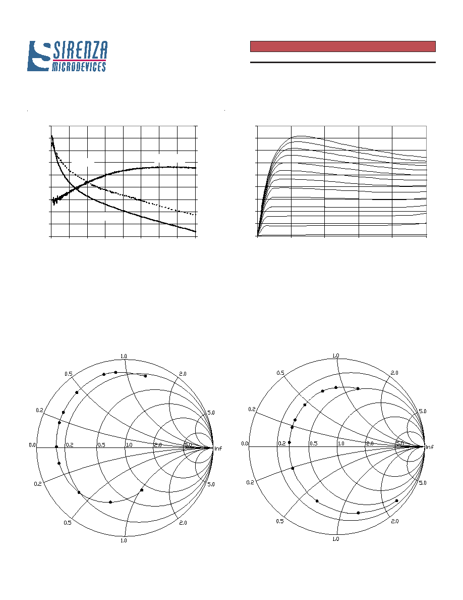
S11 Vs.
Frequency
Note: S-parameters are de-embedded to the device leads with Z
S
=Z
L
=50
. The device was mounted on Sirenza's recommended evaluation board.
De-embedded S-parameters can be downloaded from our website (www.sirenza.com)
S22 Vs.
Frequency
Typical Performance - De-embedded S-parameters
I
B
= 0.1 - 1.1 mA, T=25
∞
C
DCIV Curves
0
20
40
60
80
100
120
140
160
180
0
1
2
3
4
5
V
CE
(Volts)
I
C
(m
A
)
3.5 GHz
2.44 GHz
1.96 GHz
.88 GHz
5 GHz
.2 GHz
6 GHz
.1 GHz
.05 GHz
8 GHz
.5 GHz
3.5 GHz
2.44 GHz
1.96 GHz
.88 GHz
5 GHz
.2 GHz
6 GHz
8 GHz
.5 GHz
.1 GHz
.05 GHz
Insertion Gain & Isolation (I
CE
= 86mA)
-5
0
5
10
15
20
25
30
35
40
0
1
2
3
4
5
6
7
8
Frequency (GHz)
G
a
in, G
m
a
x
(
d
B
)
-45
-40
-35
-30
-25
-20
-15
-10
-5
0
Is
ola
t
ion (
d
B
)
Isolation
Gmax
Gain

Broomfield, CO 80021
4
EDS-102583 Rev B
Preliminary
303 S. Technology Ct.
Phone: (800) SMI-MMIC http://www.sirenza.com
SGA-8543Z Medium Power SiGe Discrete Transistor
Part Number Ordering Information
Part Identification
Pin Description
Pin #
Function
Description
1
RF IN
RF input / Base Bias. External DC blocking
capacitor required
2
GND
Connection to ground. Use via holes to
reduce lead inductance. Place via holes as
close to lead as possible
3
RF OUT
RF Out / Collector bias. External DC
blocking capacitor required
4
GND
Same as pin 2
L
C
5. DIE IS FACING UP FOR MOLD AND FACING DOWN
2.25
L
C
6. PACKAGE SURFACE TO BE MIRROR FINISH.
FOR TRIM/FORM. ie :REVERSE TRIM/FORM.
SYMBOL
4. ALL SPECIFICATIONS COMPLY TO EIAJ SC70.
2. DIMENSIONS ARE INCLUSIVE OF PLATING.
3. DIMENSIONS ARE EXCLUSIVE OF MOLD FLASH
1. ALL DIMENSIONS ARE IN MILLIMETERS.
& METAL BURR.
NOTE:
0.25
0.10
0.10
0.00
0.80
1.80
0.80
1.85
1.15
MIN
b
c
e
Q1
A2
A1
HE
A
D
E
0.65 BSC
0.40
0.18
0.40
0.10
1.00
2.40
1.10
1.35
MAX
L
0.10
0.30
b1
0.55
0.70
D
e
HE
A2
e
E
b
b1
L
C
Q1
A
A1
4
3
1
2
Part Number
Reel Size
Devices / Reel
SGA-8543Z
7"
3000
Suggested Pad Layout
85Z
1
2
3
4
Package Dimension
Use multiple plated-through vias holes located close to the
package pins to ensure a good RF ground connection to a
continuous groundplane on the backside of the board.