 | ÐлекÑÑоннÑй компоненÑ: SGC-6386Z | СкаÑаÑÑ:  PDF PDF  ZIP ZIP |
Äîêóìåíòàöèÿ è îïèñàíèÿ www.docs.chipfind.ru
Preliminary Information
Broomfield, CO 80021
1
EDS-104746 Rev A
The information provided herein is believed to be reliable at press time. Sirenza Microdevices assumes no responsibility for inaccuracies or omissions. Sirenza Microdevices assumes no responsibility for the use of this
information, and all such information shall be entirely at the user's own risk. Prices and specifications are subject to change without notice. No patent rights or licenses to any of the circuits described herein are implied or
granted to any third party. Sirenza Microdevices does not authorize or warrant any Sirenza Microdevices product for use in life-support devices and/or systems. Copyright 2005 Sirenza Microdevices, Inc.. All worldwide rights
reserved.
303 S. Technology Ct.
Phone: (800) SMI-MMIC http://www.sirenza.com
Product Description
SGC-6386Z
Pb
RoHS Compliant
&
Package
Green
50-4000 MHz Silicon Germanium
Cascadable Gain Block
Product Features
·
Single Fixed 5V Supply
·
Supply Drop Resistor not required
·
Patented Self Bias Circuitry
·
P1dB = 18.3 dBm at 1950 MHz
·
IP3 = 34.3 dBm at 1950 MHz
·
Robust 1000V ESD, Class 1C HBM
Applications
·
PA Driver Amplifier
·
Cellular, PCS, GSM, UMTS
·
IF Amplifier
·
Wireless Data, Satellite
Sirenza Microdevices' SGC-6386Z is a high performance SiGe HBT MMIC
amplifier utilizing a Darlington configuration with an active bias network. The
active bias network provides stable current over temperature and process
Beta variations. Designed to run directly from a 5V supply, the SGC-6386Z
does not require a drop resistor as compared to typical Darlington amplifiers.
The SGC-6386Z product is designed for high linearity 5V gain block
applications that require small size and minimal external components. It is
internally matched to 50 ohms.
The matte tin finish on Sirenza's lead-free "Z" package is applied using a
post annealing process to mitigate tin whisker formation and is RoHS
compliant per EU Directive 2002/95. The package body is manufactured
with green molding compounds that contain no antimony trioxide or
halogenated fire retardants.
Symbol
Parameters
Units
Frequency
Min.
Typ.
Max.
850 MHz
16.3
1950 MHz
11.9
850 MHz
19.3
1950 MHz
18.3
850 MHz
35.6
1950 MHz
34.3
IRL
Input Return Loss
dB
1950 MHz
18.0
ORL
Output Return Loss
dB
1950 MHz
17.0
NF
Noise Figure
dB
1930 MHz
4.2
V
D
Device Operating Voltage
V
5.0
I
D
Device Operating Current
mA
80
Rth, j-l
Thermal Resistance (junction to lead)
°C/W
106
Output Power at 1dB Compression
Typical performance with appropriate application circuit
dB
dBm
dBm
Z
S
= Z
L
= 50 Ohms Pout per tone = 0 dBm
Test Conditions: V
D
= 5.0V I
D
= 80mA Typ. OIP
3
Tone Spacing = 1MHz T
L
= 25°C
OIP
3
Output Third Order Intercept Point
Small Signal Gain
G
P
1dB
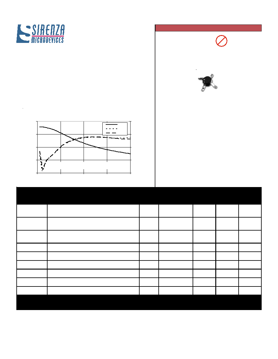
Gain & Return Loss vs. Frequency
V
D
= 5V, I
D
= 80mA (Typ.)
0
5
10
15
20
0
1
2
3
4
Frequency (GHz)
G
a
in
(d
B
)
-40
-30
-20
-10
0
Ret
u
r
n
L
o
s
s
(
d
B)
Gain
IRL
ORL
* No external components and wide band bias tee
ZS = ZL = 50 ohms, Tlead=25C
Broomfield, CO 80021
2
EDS-104746 Rev A
303 S. Technology Ct.
Phone: (800) SMI-MMIC http://www.sirenza.com
Preliminary Information
SGC-6386Z 0.05-4.0 GHz Cascadeable MMIC Amplifier
Caution: ESD sensitive
Appropriate precautions in handling, packaging
and testing devices must be observed.
Parameter
Rating
ESD Rating - Human Body Model (HBM)
Class 1C
Moisture Sensitivity Level
MSL 1
Reliability & Qualification Information
This product qualification report can be downloaded at
www.sirenza.com
100
500
850
1000
1950
2200
G
Small Signal Gain
dB
17.5
17.3
16.2
15.1
11.9
11.1
OIP
3
Output Third Order Intercept Point
dBm
35.8
36.2
35.6
34.9
34.3
33.6
P
1dB
Output Power at 1dB Compression
dBm
19.4
19.7
19.3
18.9
18.3
18.0
IRL
Input Return Loss
dB
10.0
35.0
21.0
12.0
18.0
16.0
ORL
Output Return Loss
dB
12.0
20.0
22.0
15.0
17.0
15.0
S
12
Reverse Isolation
dB
21.0
21.0
21.0
21.0
19.0
18.0
NF
Noise Figure
dB
3.1
3.3
3.4
3.5
4.2
4.3
Test Conditions: V
D
= 5V I
D
= 80mA Typ. OIP
3
Tone Spacing = 1MHz, Pout per tone = 0 dBm
T
L
= 25°C Z
S
= Z
L
= 50 Ohms
Frequency (MHz)
100 - 1000MHz App. Circuit
1000 - 2200MHz App. Circuit
Typical RF Performance at Key Operating Frequencies (Application Circuit)
Symbol
Parameter
Unit
Parameter
Absolute Limit
Max Device Current (I
CE
)
120 mA
Max Device Voltage (V
CE
)
6.5 V
Max. RF Input Power* (See Note)
+18 dBm
Max. Junction Temp. (T
J
)
+150°C
Operating Temp. Range (T
L
)
-40°C to +85°C
Max. Storage Temp.
+150°C
Absolute Maximum Ratings
Operation of this device beyond any one of these limits may cause
permanent damage. For reliable continuous operation, the device
voltage and current must not exceed the maximum operating values
specified in the table on page one.
Bias Conditions should also satisfy the following expression:
I
D
V
D
< (T
J
- T
L
) / R
TH
, j-l T
L
=T
LEAD
*Note: Load condition, Z
L
= 50 Ohms
NF vs. Frequency (V
D
= 5V, I
D
= 80mA Typ.)
2
3
4
5
6
7
0
0.5
1
1.5
2
2.5
3
3.5
4
Frequency (GHz)
NF
(
d
B)
* No external components and wide band bias tee
ZS = ZL = 50 ohms, Tlead=25C
Id vs. Vd Vs. Temperature
0
20
40
60
80
100
0.0
1.0
2.0
3.0
4.0
5.0
6.0
Vd (V)
Id (m
A
)
T=-40C
T=25C
T=85C
Broomfield, CO 80021
3
EDS-104746 Rev A
303 S. Technology Ct.
Phone: (800) SMI-MMIC http://www.sirenza.com
Preliminary Information
SGC-6386Z 0.05-4.0 GHz Cascadeable MMIC Amplifier
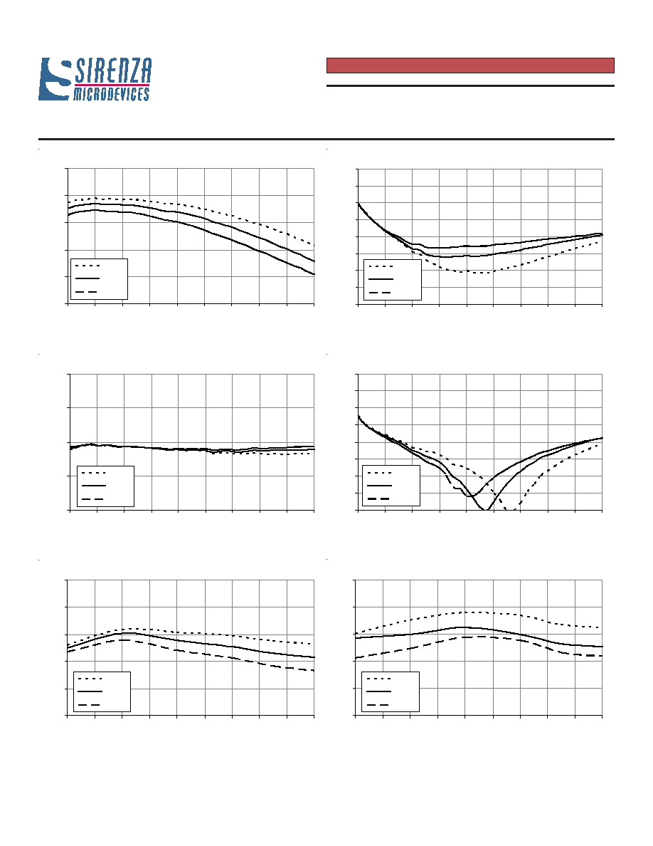
Typical RF Performance, 100-1000 MHz Application Circuit
(
Bias: V
D
= 5.0 V, I
D
= 80 mA (Typ.)
)
lS21l vs Frequency
14
15
16
17
18
19
100
200
300
400
500
600
700
800
900
1000
Frequency (MHz)
l
S
21l
(
d
B
)
T=-40C
T=25C
T=85C
lS11l vs Frequency
-40
-35
-30
-25
-20
-15
-10
-5
0
100
200
300
400
500
600
700
800
900
1000
Frequency (MHz)
l
S
11l
(
d
B
)
T=-40C
T=25C
T=85C
lS12l vs Frequency
-30
-25
-20
-15
-10
100
200
300
400
500
600
700
800
900
1000
Frequency (MHz)
T=-40C
T=25C
T=85C
lS22l vs Frequency
-40
-35
-30
-25
-20
-15
-10
-5
0
100
200
300
400
500
600
700
800
900
1000
Frequency (MHz)
l
S
22l
(
d
B
)
T=-40C
T=25C
T=85C
P1dB vs Frequency
17
18
19
20
21
22
100
200
300
400
500
600
700
800
900
1000
Frequency (MHz)
P1
d
B
(d
B
m
)
T=-40C
T=25C
T=85C
OIP3 vs Frequency
33
34
35
36
37
38
100
200
300
400
500
600
700
800
900
1000
Frequency (MHz)
OI
P
3
(
d
B
m
)
T=-40C
T=25C
T=85C
Broomfield, CO 80021
4
EDS-104746 Rev A
303 S. Technology Ct.
Phone: (800) SMI-MMIC http://www.sirenza.com
Preliminary Information
SGC-6386Z 0.05-4.0 GHz Cascadeable MMIC Amplifier
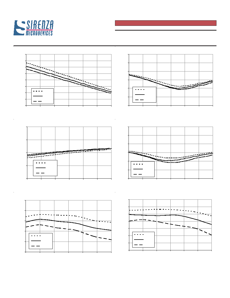
Typical RF Performance, 1000-2200 MHz Application Circuit
(
Bias: V
D
= 5.0 V, I
D
= 80 mA (Typ.)
)
lS21l vs Frequency
9
10
11
12
13
14
15
16
17
1.0
1.2
1.4
1.6
1.8
2.0
2.2
Frequency (GHz)
l
S
21l
(
d
B
)
T=-40C
T=25C
T=85C
lS11l vs Frequency
-30
-25
-20
-15
-10
-5
0
1.0
1.2
1.4
1.6
1.8
2.0
2.2
Frequency (GHz)
lS
1
1
l (
d
B
)
T=-40C
T=25C
T=85C
lS12l vs Frequency
-30
-25
-20
-15
-10
1.0
1.2
1.4
1.6
1.8
2.0
2.2
Frequency (GHz)
l
S
12l
(
d
B
)
T=-40C
T=25C
T=85C
lS22l vs Frequency
-30
-25
-20
-15
-10
-5
0
1.0
1.2
1.4
1.6
1.8
2.0
2.2
Frequency (GHz)
lS
2
2
l (
d
B
)
T=-40C
T=25C
T=85C
P1dB vs Frequency
16
17
18
19
20
21
1.0
1.2
1.4
1.6
1.8
2.0
2.2
Frequency (GHz)
P1
d
B
(d
B
m
)
T=-40C
T=25C
T=85C
OIP3 vs Frequency
30
31
32
33
34
35
36
37
1.0
1.2
1.4
1.6
1.8
2.0
2.2
Frequency (GHz)
OI
P
3
(
d
B
m
)
T=-40C
T=25C
T=85C
Broomfield, CO 80021
5
EDS-104746 Rev A
303 S. Technology Ct.
Phone: (800) SMI-MMIC http://www.sirenza.com
Preliminary Information
SGC-6386Z 0.05-4.0 GHz Cascadeable MMIC Amplifier
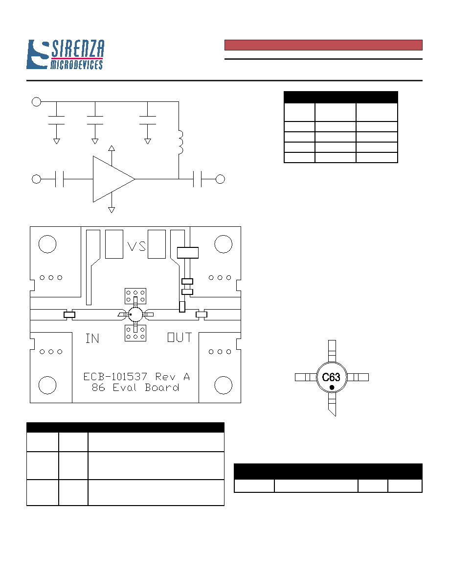
RF IN
4
1
C1
SGC-6386Z
2
3
1uF
Vs
1000pF
RF OUT
C2
C3
L1
Mounting Instructions
1. Use a large ground pad area under device pins 2
and 4 with many plated through-holes as shown.
2. We recommend 1 or 2 ounce copper. Measurements
for this data sheet were made on a 31 mil thick FR-4
board with 1 ounce copper on both sides.
Basic Application Circuit
Application Circuit Element Values
Reference
Designator
100-1000MHz
1000-2200MHz
C1
1000pF
6.8pF
C2
100pF
6.8pF
C3
100pF
6.8pF
L1
100nH
39nH
C2
C1
L1
1uF
1000pF
C3
1
2
3
4
Pin #
Function
Description
1
RF IN
RF input pin. This pin requires the use of an external DC
blocking capacitor chosen for the frequency of operation
2,4
GND
Connection to ground. Use via holes as close to the device
ground leads as possible to reduce ground inductance and
achieve optimum RF performance
3
RF OUT /
DCBIAS
RF output and bias pin. This pin requires the use of an
external DC blocking capacitor chosen for the frequency of
operation.
Part Identification Marking & Pinout
Part
Number
Package /
Lead Composition
Reel Size
Devices /
Reel
SGC-6386Z
Lead Free, RoHS Compliant
13"
3000