
The information provided herein is believed to be reliable at press time. Sirenza Microdevices assumes no responsibility for inaccuracies or omissions. Sirenza Microdevices assumes no responsibility for the use of this information, and all such
information shall be entirely at the user's own risk. Prices and specifications are subject to change without notice. No patent rights or licenses to any of the circuits described herein are implied or granted to any thrid party. Sirenza Microdevices
does not authorize or warrant any Sirenza Microdevices product for use in life-support devices and/or systems. Copyright 2005 Sirenza Microdevices, Inc. All worldwide rights reserved.
303 S. Technology Court,
Phone: (800) SMI-MMIC
http://www.sirenza.com
Broomfield, CO 80021
1
EDS-104292 Rev C
Sirenza Microdevices' SLD2000 is a robust 12 Watt, high performance
LDMOS transistor die, designed for operation from 10 to 2700MHz. It
is an excellent solution for applications requiring high linearity and effi-
ciency. The SLD2000 is typically used as a driver or output stage for
power amplifier, or transmitter applications. These robust power tran-
sistors are fabricated using Sirenza's high performance XEMOS II
TM
process.
RF Specifications
Symbol
Parameter
Unit
Min
Typ
Max
Frequency
Frequency of Operation
MHz
10
-
2700
Gain
10 Watt CW, 902 - 928MHz
dB
-
19
-
Efficiency
Drain Efficiency at 10 Watt CW, 915MHz
%
-
47
-
Linearity
3
rd
Order IMD at 10 Watt PEP (Two Tone), 915MHz
dBc
-
-32
-
Linearity
1dB Compression (P
1dB
)
W
-
12
-
R
TH
Thermal Resistance (Junction-to-Case, mounted in package)
�C/W
-
4
-
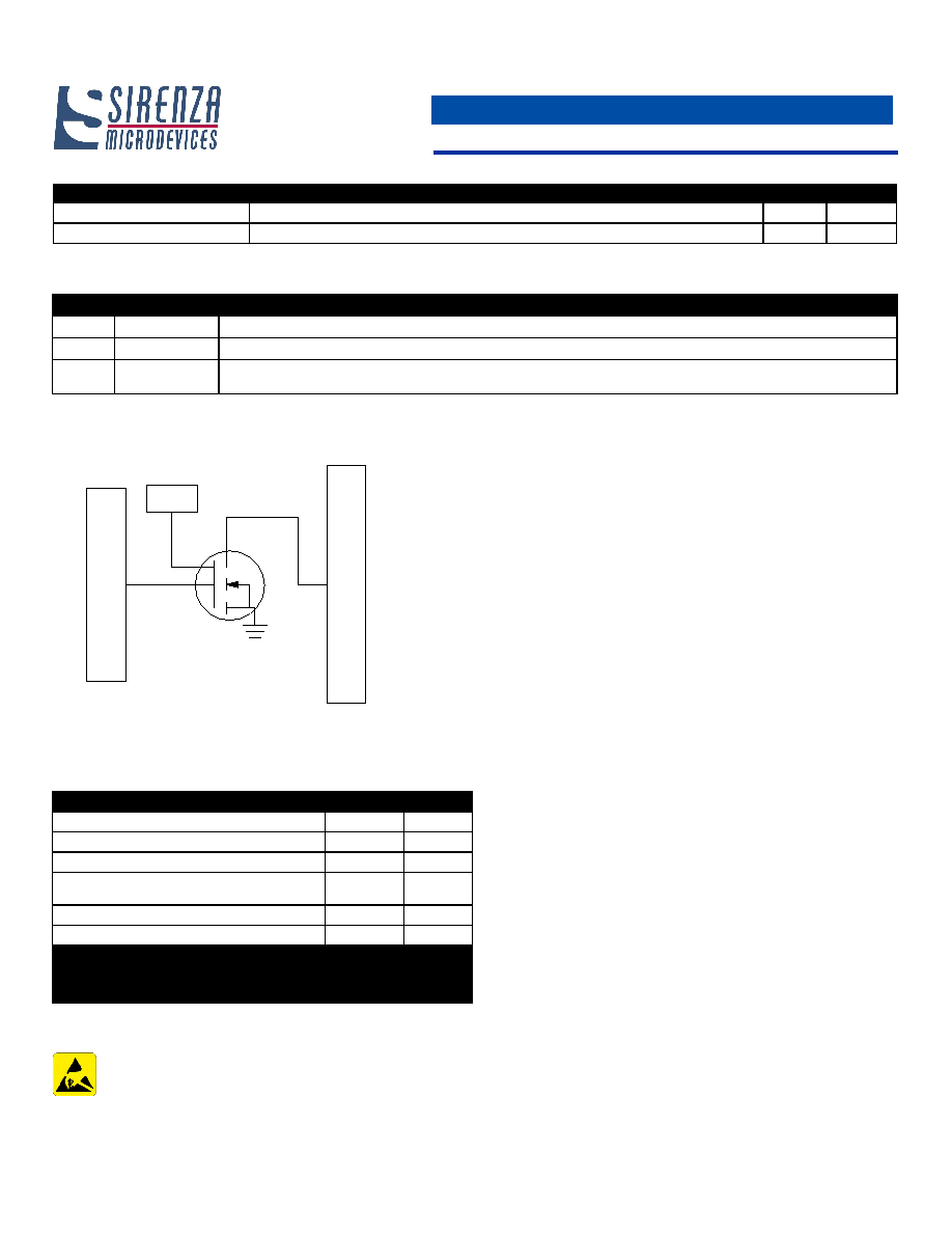
Functional Schematic Diagram
SLD-2000
12 Watt Discrete LDMOS FET -Bare Die
Product Features
Applications
�
12 Watt Output P
1dB
�
Single Polarity Operation
�
19dB Gain at 900 MHz
�
XeMOS II
TM
LDMOS
�
Integrated ESD Protection, Class 1B
�
Aluminum Topside Metallization
�
Gold Backside Metallization
�
Base Station PA Driver
�
Repeaters
�
Military Communications
�
RFID
�
GSM, CDMA, Edge, WDCDMA
Product Description
Drain
Manifold
Gate
Manifold
Source - Backside Contact
ESD
Protection
Test Conditions: Mounted in ceramic package and tested in Sirenza Evaluation Board V
DS
= 28.0V, I
DQ
= 150mA, T
Mounting Surface
= 25�C
T
DC Specifications
Symbol
Parameter
Unit
Min
Typical
Max
g
m
Forward Transconductance @ 125mA I
DQ
, V
DS
=28V
mA / V
590
V
GS
Threshold
I
DS
=3mA
V
3.0
3.8
5.0
V
DS
Breakdown
1mA V
DS
current
V
65
70
C
iss
Input Capacitance (Gate to Source) V
GS
=0V, V
DS
=28V
pF
27.5
C
rss
Reverse Capacitance (Gate to Drain) V
GS
=0V, V
DS
=28V
pF
0.8
C
oss
Output Capacitance (Drain to Source) V
GS
=0V, V
DS
=28V
pF
14.7
R
DSON
Drain to Source Resistance, V
GS
=10V V
DS
=250mV
R
0.6
0.75
SLD-2000 10-2700 MHz 12 Watt LDMOS FET - Bare Die
303 S. Technology Court
Phone: (800) SMI-MMIC
http://www.sirenza.com
Broomfield, CO 80021
2
EDS-104292 Rev C
Pad #3
Backside Source = Ground
ESD
Protection
Pad #1
Gate
Manifold
Pad #2
Drain
Manifold
Contact Description
Pad #
Function
Description
1
Gate
Aluminum metallized manifold MOSFET Gate with ESD protection structure. (Topside contact)
2
Drain
Aluminum metallized manifold MOSFET Drain. (Topside contact)
3
Source
Chrome Gold metallized MOSFET Source contact. Appropriate electrical, mechanical and thermal connection required for
proper operation. (Backside contact)
Absolute Maximum Ratings
Parameters
Value
Unit
Drain Voltage (V
DS
)
35
Volts
Gate Voltage (V
GS
), V
DS
=0
20
Volts
RF Input Power
+33
dBm
Load Impedance for Continuous Operation
Without Damage
10:1
VSWR
Output Device Channel Temperature
+200
�C
Storage Temperature Range
-40 to +150
�C
Operation of this device beyond any one of these limits may cause
permanent damage. For reliable continuous operation see typical
setup values specified in the table on page one.
Caution: ESD Sensitive
Appropriate precaution in handling, packaging
and testing devices must be observed.
Quality Specifications
Parameter
Description
Unit
Typical
ESD Rating
Human Body Model
Volts
750
MTTF
200
o
C Channel
Hours
1.2 X 10
6
Pad Diagram
Note 1:
Gate voltage must be applied to to the device
concurrently or after application of drain voltage to
prevent potentially destructive oscillations. Bias voltages should
never be applied to the transistor unless it is properly termi-
nated on both input and output.
Note 2:
The required V
GS
corresponding to a specific I
DQ
will vary from
device to device due to the normal die-to-die variation in thresh-
old voltage with LDMOS transistors.
Note 3:
The threshold voltage (V
GSTH
) of LDMOS transistors varies with
device temperature. External temperature compensation may
be required. See Sirenza application notes AN-067 LDMOS
Bias Temperature
Compensation.

SLD-2000 10-2700 MHz 12 Watt LDMOS FET - Bare Die
303 S. Technology Court
Phone: (800) SMI-MMIC
http://www.sirenza.com
Broomfield, CO 80021
3
EDS-104292 Rev C
De-embedding Information
Description
Gate
Drain
Number of Bond Wires
6
9
Length of Bond Wires
0.037
0.040
Height of Bond Wires
0.006
0.007
Pitch of Bond Wires
0.012
0.008
Bond Wire Diameter
0.002
0.002
Impedance Data
Frequency (MHz)
Z
source
Z
load
880
0.5 + j 2.5
3.9 + j 4.9
960
0.8 + j 1.3
4.5 + j 3.6
1840
0.7 - j 0.4
1.3 + j 0.0
1960
0.5 -j 1.3
1.3 + j 0.1
2140
0.7 - j 2.3
1.2 + j 0.2
Impedances Referenced to Wirebond/PCB Interface.
All Dimensions in Inches.
Wirebond Heights Referenced to Top Surface of Die.
Zload
source
Z
Input
Matching
Network
Output
Matching
Network
Device
under test
Z
source
and Z
load
are the optimal
impedances presented to the SLD-
2000
when operating at 28V,
Idq=150mA, Pout=10 W PEP.

SLD-2000 10-2700 MHz 12 Watt LDMOS FET - Bare Die
303 S. Technology Court
Phone: (800) SMI-MMIC
http://www.sirenza.com
Broomfield, CO 80021
4
EDS-104292 Rev C
Typical Performance Curves for packaged die tested in SLD-2083CZ 900 MHz Application Circuit
2 Tone Gain, Efficiency, Linearity vs Pout
Vdd=28V, Idq=125mA, Freq=915 MHz, Delta F=1 MHz
0
5
10
15
20
25
30
35
40
45
1
3
5
7
9
11
13
Pout (W PEP)
G
a
i
n
(
d
B
)
,
E
f
f
i
ci
e
n
cy
(
%
)
-70
-65
-60
-55
-50
-45
-40
-35
-30
-25
IM
D
(
d
B
c
)
Gain
Efficiency
IM3
IM5
IM7
CW Gain, Efficiency vs Pout
Vdd=28V, Idq=125mA, Freq=915 MHz
15
16
17
18
19
20
21
22
23
24
25
0
2
4
6
8
10
12
14
16
Pout (W)
Ga
i
n
(
d
B
)
10
15
20
25
30
35
40
45
50
55
60
E
ffici
e
n
c
y (
%
)
Gain
Efficiency
CW Gain, Efficiency, IRL vs Frequency
Vdd=28V, Idq=125mA, Pout=10W
0
10
20
30
40
50
60
900
905
910
915
920
925
Frequency (MHz)
G
a
i
n
(
d
B
)
,
E
f
f
i
ci
e
n
cy
(
%
)
-24
-20
-16
-12
-8
-4
0
I
nput
R
e
t
u
r
n
Los
s
(
d
B
)
Gain
Efficiency
IRL
2 Tone Gain, Efficiency, Linearity and IRL vs Frequency
Vdd=28V, Idq=125mA, Pout=10W PEP, Delta F=1 MHz
0
10
20
30
40
50
60
900
905
910
915
920
925
Frequency (MHz)
G
a
i
n
(
d
B
)
, E
ffi
c
i
e
n
c
y
(
%
)
-60
-50
-40
-30
-20
-10
0
IMD
(
d
B
c
)
,
IR
L
(d
B
)
Gain
Efficiency
IM3
IM5
IM7
IRL

SLD-2000 10-2700 MHz 12 Watt LDMOS FET - Bare Die
303 S. Technology Court
Phone: (800) SMI-MMIC
http://www.sirenza.com
Broomfield, CO 80021
5
EDS-104292 Rev C
Die Map
AuSi, AuSn, or AuGe eutectic die attach is recommended. AlSi bond wires are recommended.
Part Number Ordering Information
Die are screened prior to dicing to DC parameters and
are shipped per Sirenza application note AN-039
Visual Criteria of Unpackaged Die.
Part Number
Gel Pack
SLD-2000
100 pcs. per pack
Dimensions Inches [mm]
0.0850 [2.16]
0.0450 [1.14]
GATE
DRAIN
SOURCE - BACKSIDE CONTACT - NOT SHOWN
DIE THICKNESS - 0.004 [0.10]