 | –≠–ª–µ–∫—Ç—Ä–æ–Ω–Ω—ã–π –∫–æ–º–ø–æ–Ω–µ–Ω—Ç: SPA-1118Z | –°–∫–∞—á–∞—Ç—å:  PDF PDF  ZIP ZIP |
The information provided herein is believed to be reliable at press time. Sirenza Microdevices assumes no responsibility for inaccuracies or omissions. Sirenza Microdevices assumes no responsibility for the use of this
information, and all such information shall be entirely at the user's own risk. Prices and specifications are subject to change without notice. No patent rights or licenses to any of the circuits described herein are implied or
granted to any third party. Sirenza Microdevices does not authorize or warrant any Sirenza Microdevices product for use in life-support devices and/or systems. Copyright 2002 Sirenza Microdevices, Inc. All worldwide rights
reserved.
1
Product Description
EDS-101427 Rev I
Phone: (800) SMI-MMIC
http://www.sirenza.com
303 S. Technology Court, Broomfield, CO 80021
SPA-1118
SPA-1118Z
Pb
RoHS Compliant
&
Package
Green
850 MHz 1 Watt Power Amplifier
with Active Bias
Product Features
∑ Now available in Lead Free, RoHS
Compliant, & Green Packaging
∑ High Linearity Performance:
+21 dBm IS-95 Channel Power at -55 dBc ACP
+48 dBm OIP3 Typ.
∑ On-chip Active Bias Control
∑ Patented High Reliability GaAs HBT Technology
∑ Surface-Mountable Plastic Package
Applications
∑
Multi-Carrier Applications
∑
AMPS, ISM Applications
Sirenza Microdevices' SPA-1118 is a high efficiency GaAs
Heterojunction Bipolar Transistor (HBT) amplifier housed in
a low-cost surface-mountable plastic package. These HBT
amplifiers are fabricated using molecular beam epitaxial
growth technology which produces reliable and consistent
performance from wafer to wafer and lot to lot.
This product is specifically designed for use as a driver
amplifier for infrastructure equipment in the 850 MHz band.
Its high linearity makes it an ideal choice for wireless data and
digital applications.
The matte tin finish on Sirenza's lead-free package utilizes a
post annealing process to mitigate tin whisker formation and
is RoHS compliant per EU Directive 2002/95. This package
is also manufactured with green molding compounds that
contain no antimony trioxide nor halogenated fire retardants.
S ym b o l
P aram eters: Test C o n d itio n s:
Z
0
= 50 Oh m s, V
C C
= 5V, Tem p = 25∫C
U n its
M in .
Typ .
M ax.
f
0
F requency of Operation
M Hz
810
960
P
1dB
Output P ower at 1dB C om pression
dB m
29.5
A C P
A djacent C hannel P ower
IS -95 @ 880 M Hz, ±885 K Hz, P
OUT
= 21 dB m
dB c
-57.0
-54.0
S
21
S m all S ignal Gain, 880 M Hz
dB
16.2
17.2
18.2
V S W R
Input V S W R
-
1.5:1
OIP
3
Output Third Order Intercept P oint
P ower out per tone = +14 dB m
dB m
48.0
NF
Noise F igure
dB
7.5
I
C C
D evice C urrent
m A
275
310
330
V
C C
D evice Voltage
V
4.75
5.0
5.25
R
th,
j-l
Therm al Resistance (junction - lead) , T
L
=85∫C
∫C /W
35
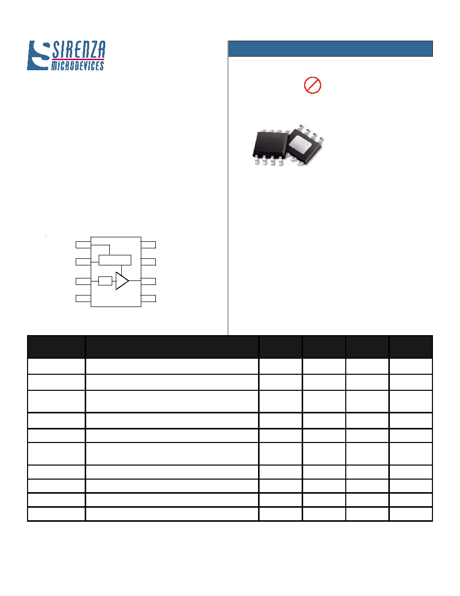
VCC
VBIAS
RFIN
N/C
RFOUT/
VCC
Active Bias
Input
Match
N/C
N/C
N/C

2
SPA-1118 850 MHz 1 Watt Power Amp.
EDS-101427 Rev I
Phone: (800) SMI-MMIC
http://www.sirenza.com
303 S. Technology Court, Broomfield, CO 80021
20
22
24
26
28
30
32
0.85
0.87
0.89
0.91
0.93
0.95
25C
85C
-40C
10
12
14
16
18
20
22
0.85
0.8 7
0.8 9
0 .91
0 .93
0.95
2 5C
8 5C
-40C
-4 0
-3 5
-3 0
-2 5
-2 0
-1 5
-1 0
-5
0
0 .8 5
0 .8 7
0.89
0.91
0 .93
0.95
S 1 1
S 1 2
S 2 2
-75
-70
-65
-60
-55
-50
-45
17
18
19
20
21
22
23
24
-40C
85C
25C
P1dB vs. Frequency
GHz
dBm
850-950 MHz Application Circuit Data, I
CC
=320 mA, V
CC
=5V
IS-95 @ 880 MHz
Adj. Channel Pwr. vs. Channel Output Pwr.
dBm
dBc
GHz
Gain vs. Frequency
dB
Input/Output Return Loss,
Isolation vs. Frequency, T=25
∞
C
GHz
dB
0
50
100
150
200
250
300
350
400
450
0
1
2
3
4
5
25C
-40C
85C
Device Current vs. Source Voltage
V
cc
(V)
Device Current (mA)
SPA-1118 850 MHz 1 Watt Power Amp.
3
EDS-101427 Rev I
Phone: (800) SMI-MMIC
http://www.sirenza.com
303 S. Technology Court, Broomfield, CO 80021
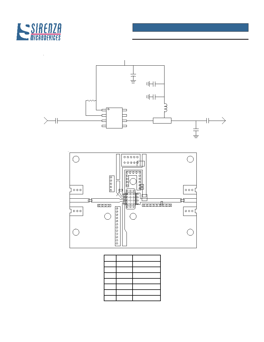
VCC
5.6 pF
100 nH
43pF
10uF,
Tantalum
22pF
22pF
Z=50
, 17∞
360
1
2
3
4
8
7
6
5
1000pF
850 - 950 MHz Schematic
850 - 950 MHz Evaluation Board Layout
Vpc
Vcc
SOIC-8 PA
ECB-101161 Rev. C
Eval Board
C5
L1
C4
C3
C2
C1
C6
R1
Note: Pins 4, 5, 7, 8 are not
connected internally
Sirenza Microdevices
Ref. Des.
Value
Part Number
C1, C6
22pF, 5%
Rohm MCH18 series
C2
10uF, 10%
AVX TAJB106K020R
C3
1000pF, 5%
Rohm MCH18 series
C4
43pF, 5%
Rohm MCH18 series
C5
5.6pF, ±0.5pF
Rohm MCH18 series
L1
100nH, 5%
Coilcraft 1008HQ series
R1
360 Ohm, 5%
Rohm MCR03 series

4
SPA-1118 850 MHz 1 Watt Power Amp.
EDS-101427 Rev I
Phone: (800) SMI-MMIC
http://www.sirenza.com
303 S. Technology Court, Broomfield, CO 80021
Pin #
Function
Description
Device Schematic
1
Vcc
VCC is the supply voltage for the active bias network.
Bypassing in the appropriate location as shown on
application schematic is required for optimum RF
performance.
2
Vbias
Vbias is the bias control pin for the active bias network.
Device current is set by the current into this pin.
Recommended configuration is shown in the Application
Schematic. Bypassing in the appropriate location as
shown on application schematic is required for optimum
RF performance.
3
RF In
RF input pin. This pin requires the use of an external
DC blocking capacitor chosen for the frequency of
operation.
4, 5
N/C
No connection
6
RF Out/Vcc RF output and bias pin. Bias should be supplied to this
pin through an external RF choke. Because DC biasing
is present on this pin, a DC blocking capacitor should
be used in most applications (see application
schematic). The supply side of the bias network should
be well bypassed. An output matching network is
necessary for optimum performance.
7, 8
N/C
No connection
EPAD
Gnd
Exposed area on the bottom side of the package needs
to be soldered to the ground plane of the board for
thermal and RF performance. Several vias should be
located under the EPAD as shown in the recommended
land pattern (page 5).
2
3
1
6
ACTIVE BIAS
NETWORK
4,5,7,8 N/C
Absolute Maximum Ratings
Parameter (Ta = 25∫C)
Absolute
Limit
Max. Supply Current (I
CC
) at V
CC
typ.
750 mA
Max. Device Voltage (V
CC
) at I
CC
typ.
6.0 V
Max. RF Input Power
24 dBm
Max. Junction Temp. (T
J
)
+160 ∫C
Max. Storage Temp.
+150 ∫C
Operation of this device beyond any one of these limits may cause
permanent damage. For reliable continuous operation, the device
voltage and current must not exceed the maximum operating values
specified in the table on page one.
Bias Conditions should also satisfy the following expression:
I
CC
V
CC
(max) < (T
J
- T
L
)/R
th
,j-l
Caution: ESD sensitive
Appropriate precautions in handling,
packaging and testing devices must be
The Moisture Sensitivity Level rating for this device
is level 1 (MSL-1) based on the JEDEC 22-A113
standard classification. No special moisture
packaging/handling is required during storage,
shipment, or installation of the devices.

SPA-1118 850 MHz 1 Watt Power Amp.
5
EDS-101427 Rev I
Phone: (800) SMI-MMIC
http://www.sirenza.com
303 S. Technology Court, Broomfield, CO 80021
Part Number Ordering Information
Package Outline Drawing
(See SMDI MPO-101644 for tolerances, available on our website)
Recommended Land Pattern
Note: DIMENSIONS ARE IN INCHES [MM]
DETAIL A
.061 [1.549]
.155 [3.937]
.025
.013 [.33] x 45∞
.008
.003 [.076]
SEATING PLANE
BOTTOM VIEW
.058 [1.473]
TOP VIEW
SIDE VIEW
END VIEW
PARTING LINE
.008 [.203]
.194 [4.93]
.016 [.406]
.050 [1.27]
.194 [4.928]
5∞
SEE DETAIL A
EXPOSED PAD
.045 [1.143]
.035 [.889]
.236 [5.994] .155 [3.937]
1
3
2
4
8
7
6
5
Beveled Edge
0.020 [0.51]
0.140 [3.56]
0.080 [2.03]
0.050 [1.27]
0.150 [3.81]
0.300 [7.62]
Plated-Thru Holes
(0.015" Dia, 0.030" Pitch)
Machine
Screws
Lot ID
SPA
1118
Part Number
Reel Size
Devices/Reel
SPA-1118
7"
500
SPA-1118Z
7"
500
Part Identification Marking
Lot ID
SPA-1118Z
Lot ID
SPA-1118