 | –≠–ª–µ–∫—Ç—Ä–æ–Ω–Ω—ã–π –∫–æ–º–ø–æ–Ω–µ–Ω—Ç: SZA-6044 | –°–∫–∞—á–∞—Ç—å:  PDF PDF  ZIP ZIP |

The information provided herein is believed to be reliable at press time. Sirenza Microdevices assumes no responsibility for inaccuracies or ommisions.
Sirenza Microdevices assumes no responsibility for the use of this information, and all such information shall be entirely at the user's own risk. Prices and specifications are subject to change without
notice. No patent rights or licenses to any of the circuits described herein are implied or granted to any third party. Sirenza Microdevices does not authorize or warrant any Sirenza Microdevices product
for use in life-support devices and/or systems.
Copyright 2002 Sirenza Microdevices, Inc. All worldwide rights reserved.
303 South Technology Court Broomfield, CO 80021
Phone: (800) SMI-MMIC
http://www.sirenza.com
1
EDS-103535 Rev E
Preliminary
Sirenza Microdevices' SZA-6044 is a high linearity Class A
GaAs Heterojunction Bipolar Transistor (HBT) amplifier
housed in a low-cost surface-mountable plastic package.
These HBT amplifiers are fabricated using molecular beam
epitaxial growth technology which produces reliable and
consistent performance from wafer to wafer and lot to lot.
This product is specifically designed as a driver or final
stage amplifier for equipment in the 5.1 - 5.9 GHz band. It
can run from a 3V to 5V supply. Load line optimization for
target band is possible outside the package. Its high lin-
earity makes it an ideal choice for multicarrier and digital
applications.
Key Specifications
Symbol
Parameters: Test Conditions, With App Circuit
Z
0
= 50
, V
CC
= 5.0V, I = 165mA, T
BP
= 30∫C)
Unit
Min.
Typ.
Max.
f
O
Frequency of Operation
MHz
5100
5900
P
1dB
Output Power at 1dB Compression ≠ 5.1 GHz
dBm
24.9
Output Power at 1dB Compression ≠ 5.5 GHz
24.6
Output Power at 1dB Compression ≠ 5.9 GHz
22.5
24.0
26.0
S
21
Small Signal Gain ≠ 5.1 GHz
dB
17.0
18.5
20.0
Small Signal Gain ≠ 5.5 GHz
17.3
Small Signal Gain ≠ 5.9 GHz
14.9
16.4
17.9
IRL
Worst Case Input Return Loss 5.1-5.9GHz
dB
8
11
ORL
Worst Case Output Return Loss 5.1-5.9GHZ
dB
12
17
OIP
3
Output IP3, Pout per tone = +8dBm @ 5.9 GHz
dBm
37
39
Pout
802.11a 54Mb/s Pout @ 3% EVM @ 5.9GHz, I = 165mA
dBm
17
NF
Noise Figure @ 5.9 GHz
dB
7.8
9.8
I
SUPPLY
Total Device Current, I
VBIAS
+ I
CTOTAL
= 150mA
I
VPC12
= 15mA
mA
145
165
185
R
th, j-l
Thermal Resistance (junction - lead)
∫C/W
56
Functional Block Diagram
SZA-6044
5.1 ≠ 5.9 GHz º Watt
Power Amplifier with Active Bias
Product Features
Applications
∑
Single 3V to 5V operation
∑
High Linearity Class A OIP3 = 39dBm @ 5V
∑
802.11a 54Mb/s Pout = 17dBm @ 3% EVM
∑
P1dB 24dBm @ 5V, 21dBm @ 3.3V
∑
Surface Mount Plastic Package
∑
Power up/down control < 1
µ
s
∑
OFDM
∑
Multicarrier applications
∑
802.11a WLAN Driver Stage
∑
Fixed Wireless, UNII
Product Description
4mm x 4mm
QFN Package
VC1
VPC2
NC
NC
NC
NC
Vbias
NC
VPC1
RFIN
RFOUT
NC
NC
RFOUT
RFOUT
RFIN
NC
NC
NC
NC
1
2
3
4
5
6
7
9
8
10
11
12
13
14
15
16
17
18
19
20
Active
Bias

303 South Technology Court Broomfield, CO 80021
Phone: (800) SMI-MMIC
http://www.sirenza.com
2
EDS-103535 Rev E
Preliminary
SZA-6044 5.1-5.9 GHz º W Amplifier
Pin Out Description
Pin #
Function
Description
1,2,5,6,
7,8,9,10,
11,15,16
N/C
Pins are not used. May be grounded, left open or connected to adjacent pin.
19
VPC2
VPC2 is the bias control pin for the stage 2 active bias circuit. An external series resistor is required for proper
setting of bias levels. Refer to the evaluation board schematic for resistor value.
20
VPC1
VPC1 is the control pin for the stage 1 active bias circuits. An external series resistor is required for proper set-
ting of bias levels. Refer to the evaluation board schematic for resistor value.
18
VBIAS
VBIAS is the active bias circuit supply voltage. Can be operated from 3V to 5V.
3,4
RFIN
RF input pin. This is DC grounded internal to the IC. Do not apply voltage to this pin. Both pins 3 and 4 must be
used for proper operation.
12,13,14
RFOUT/
VC2
RF output and second stage collector supply voltage pin. VC2 in the range of 3V to 5V voltage should be sup-
plied to this pin through an external RF choke. Because DC biasing is present on this pin, a DC blocking
capacitor should be used in most applications (see evaluation board schematic). The supply side of the bias
network should be well bypassed. The output network and board layout specified in the app circuit is recom-
mended for optimum performance. All pins 12-14 are required to be wired together at lead foot for proper
operation.
17
VC1
VC1 is the first stage collector supply voltage. Can be operated over the range of 3V to 5V.
EPAD
Gnd
Exposed area on the bottom side of the package needs to be soldered to the ground plane of the board for
optimum thermal and RF performance. Several vias should be located under the EPAD as shown in the rec-
ommended land pattern (page 5).
Caution: ESD Sensitive - Class 1B
Appropriate precaution in handling, packaging
and testing devices must be observed.
Absolute Maximum Ratings
Parameters
Value
Unit
1st Stage Collector Bias Current (I
VC1
)
100
mA
2nd Stage Collector Bias Current (I
VC2
)
190
mA
Device Voltage (V
D
)
6.0
V
Power Dissipation
1.5
W
Operating Lead Temperature (T
L
)
-40 to +85
∫C
RF Input Power
20
dBm
Storage Temperature Range
-40 to +150
∫C
Operating Junction Temperature (T
J
)
+150
∫C
ESD Human Body Model - Class 1B
500
V
Operation of this device beyond any one of these limits may
cause permanent damage. For reliable continuous operation
the device voltage and current must not exceed the maximum
operating values specified in the table on page one.
Bias conditions should also satisfy the following expression:
I
D
V
D
< (T
J
- T
L
) / R
TH'
j-l
Simplified Device Schematic
3
4
Active
Bias
20
17
Active
Bias
19
18
12
13
14
VC1
Q1
Q2
1
2
5
6
7
8
N/C
VPC1
RF IN
VPC2
RF OUT/
VC2
VBIAS
9
10
11
15
16

303 South Technology Court Broomfield, CO 80021
Phone: (800) SMI-MMIC
http://www.sirenza.com
3
EDS-103535 Rev E
Preliminary
SZA-6044 5.1-5.9 GHz º W Amplifier
5.1 - 5.9 GHz Evaluation Board Data (V
BIAS
= 5.0V, I
BIAS
= 165mA)
Input/Output Return Loss, Isolation vs Frequency +25c
-45
-40
-35
-30
-25
-20
-15
-10
5100
5200
5300
5400
5500
5600
5700
5800
5900
Frequency(MHz)
Return Loss (dB)
S12
S22
S11
Device Current vs Source Voltage
0.00
0.05
0.10
0.15
0.20
0.25
0.30
0
1
2
3
4
5
6
Vcc(V)
Device Current(A)
+25c
-40c
+85c
Gain vs Temp
12
13
14
15
16
17
18
19
20
21
22
5100
5200
5300
5400
5500
5600
5700
5800
5900
Frequency(MHz)
Gain (dB)
+25c
-40c
+85c
Output Thrid Order Intercept vs Frequency (Pout/tone =
2dBm)
32.0
33.0
34.0
35.0
36.0
37.0
38.0
39.0
40.0
41.0
42.0
5100
5200
5300
5400
5500
5600
5700
5800
5900
Frequency (MHz)
OIP3 (dBm)
+25c
-40c
+85c
Broadband Gain, Input/Output
Return Loss vs Frequency +25c
-35
-25
-15
-5
5
15
25
1
2
3
4
5
6
Frequency (GHz)
dB
S11
S21
S22
P1dB vs Frequency
23.0
23.3
23.5
23.8
24.0
24.3
24.5
24.8
25.0
25.3
25.5
25.8
26.0
5100
5300
5500
5700
5900
Frequency (MHz)
P1 (dBm)
+25c
-40c
+85c
303 South Technology Court Broomfield, CO 80021
Phone: (800) SMI-MMIC
http://www.sirenza.com
4
EDS-103535 Rev E
Preliminary
SZA-6044 5.1-5.9 GHz º W Amplifier
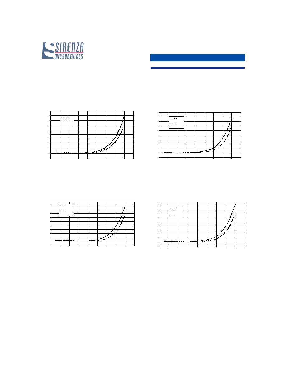
802.11a 64QAM 54Mb/s Error Vector Magnitude Data (V
BIAS
= 5.0V, I
BIAS
= 165mA)
EVM Burst Average% vs Output Power (dBM)
Freq = 5.35GHz
0
0.5
1
1.5
2
2.5
3
3.5
4
4.5
5
2
4
6
8
10
12
14
16
18
20
Output power (dBm)
BAVG%
+25c
-40c
+85c
EVM Burst Average% vs Output Power (dBM)
Freq = 5.725GHz
0
0.5
1
1.5
2
2.5
3
3.5
4
4.5
5
5.5
2
4
6
8
10
12
14
16
18
20
Output power (dBm)
BAVG%
+25c
-40c
+85c
EVM Burst Average% vs Output Power (dBM)
Freq = 5.875GHz
0
0.5
1
1.5
2
2.5
3
3.5
4
4.5
5
5.5
2
4
6
8
10
12
14
16
18
20
Output power (dBm)
BAVG%
+25c
-40c
+85c
EVM Burst Average% vs Output Power (dBM)
Freq = 5.15GHz
0
0.5
1
1.5
2
2.5
3
3.5
4
4.5
5
2
4
6
8
10
12
14
16
18
20
Output power (dBm)
BAVG%
+25c
-40c
+85c

303 South Technology Court Broomfield, CO 80021
Phone: (800) SMI-MMIC
http://www.sirenza.com
5
EDS-103535 Rev E
Preliminary
SZA-6044 5.1-5.9 GHz º W Amplifier
5.1 - 5.9 GHz Evaluation Board Schematic For 5V Supply
RF INPUT INTERNALLY
GROUND. USE DC BLOCK
IF EXTERAL DC VOLTAGE
IS PRESENT.
V
8
Zo=50 ,54.2 @ 5.5GHz
,22.3
Zo=29
V
@ 5.5GHz
8
,38.4
Zo=29
V
@ 5.5GHz
8
,16
Zo=13
V
@ 5.5GHz
8
C5
C1
C4
C2
Q1
L1
R2
R1
C3
5.1 - 5.9 GHz Evaluation Board Layout For 5V - Board material GETEK, 31mil thick, Dk=3.9, 2 oz. copper
Note: For 3.3V 140mA operation, lower V+ to 3.3V and change R1 and R2 to 50 ohm.
RF Performance at 3.3V, 140mA: Gain increases 0.5dB, IP3 drops ~ 3dB and P1dB drops ~3dB relative to 5V data.
Return loss is essentially unchanged relative to 5V data. Contact factory for more details.