
ST
Sitronix
ST2064
PRELIMINARY
8 BIT Microcontroller with 64K bytes ROM
Notice: This is not a final specification. Some parameters are subject to change.
Ver 1.0
1
/
46 10/11/02
1
1
.
.
F
F
E
E
A
A
T
T
U
U
R
R
E
E
S
S
Totally static 65C02S CPU
ROM: 64K x 8-bit
RAM: 2K x 8-bit
Stack: Up to 128-level deep
Operation voltage: 2.4V ~ 3.4V
Built-in double DC-DC voltage converter for LCD driver
I/O
ports
- 24 CMOS bidirectional bit programmable I/O pins,
sixteen (Port-B/C) are shared with LCD drives
- Bit programmable pull-up for input pins
- Hardware de-bounce option for Port-A
Low voltage detector
Timer/Counter:
- Two 8-bit timer/16-bit event counter
- One 8-bit Base timer
6 hardware interrupts with dedicated exception vectors
- External interrupt (edge triggered)
- Timer0 interrupt
- Timer1 interrupt
- Base timer interrupt
- Port-A[7~0] interrupt (transition triggered)
- DAC reload interrupt
Dual clock sources with warm-up timer
- Low frequency crystal oscillator
����������������������������������������������������32768 Hz
- RC oscillator ������������������������������������������� 500K ~ 4M Hz
- High frequency crystal/resonator oscillator (code option)
���������������������������������������������� 455K~4M Hz
LCD
controller/driver
- Resolution: 32x16 ~ 48x16, maximum 768 dots
- Two clock source options: RC and resonator oscillator
- Internal bias resistors (1/5 bias) with 16-level driving
strength control
- Up to 12-level contrast control
- Keyboard scan function supported on 16 shared
segment drives
Programmable sound generator (PSG)
- Two channels with three playing modes
- Tone/noise generator
- 16-level volume control
- Dedicated outputs for directly connection to buzzer
PWM DAC: Three modes up to 8-bit resolution
Three power down modes:
- WAI0 mode
- WAI1 mode
- STP mode
2
2
.
.
G
G
E
E
N
N
E
E
R
R
A
A
L
L
D
D
E
E
S
S
C
C
R
R
I
I
P
P
T
T
I
I
O
O
N
N
The ST2064 is a W65C02S based 8-bit microcontroller
designed with CMOS silicon gate technology. This single chip
microcontroller is useful for translator, databank and other
consumer applications. It integrates with SRAM, mask ROM,
LCD controller/driver, DC-DC voltage converter, I/O ports,
timers, PSG and PWM DAC. This chip also builds in dual
oscillators for the chip performance enhancement.

Sitronix ST2064
Ver 1.0
2/46
10/11/02
3
3
.
.
P
P
A
A
D
D
D
D
I
I
A
A
G
G
R
R
A
A
M
M
1
2
3
4
5
6
7
8
9
10
11
12
13
14
15
16
17
18
19
20
21
22
23
24
25
26
27
28
29
30
31
32
33
34
35
36
37
38
39
40
41
42
43
44
45
46
47
48
49
50
51
52
53
54
55
56
57
58
59
60
61
62
63
64
65
66
67
68
69
70
71
72
73
74
75
76
77
78
79
80
81
82
83
84
85
86
87
88
89
ST2064
X
Y
CHIP SIZE : 2660um X 2930um
(0,0)
PAD SIZE : 90um X 90um
OSCXO
OSCXI
RESET
OSCI
XIO
GND
VDD
PA0
PA1
PA2
PA3
PA4
PA5
PA6
PA7
CAP1+
CAP1-
V4
V3
V2
V1
VP
COM0
COM1
COM2
COM3
COM4
COM5
COM6
COM7
COM8
COM9
COM10
COM11
COM12
COM13
COM14
COM15
SEG0
SEG1
SEG2
SEG3
SEG4
SEG5
SEG6
SEG7
SEG8
SEG9
SEG10
SEG11
SEG12
SEG13
SEG14
SEG15
SEG16
SEG17
SEG18
SEG19
SEG20
SEG21
SEG22
SEG23
SEG24
SEG25
SEG26
SEG27
SEG28
SEG29
SEG30
SEG31
SEG32/PC0
SEG33/PC1
SEG34/PC2
SEG35/PC3
SEG36/PC4
SEG37/PC5
SEG39/PC7
SEG38/PC6
SEG40/PB0
SEG41/PB1
SEG42/PB2
SEG43/PB3
SEG44/PB4
SEG45/PB5
SEG46/PB6
SEG47/PB7
PSGOB
PSGO
TEST

Sitronix ST2064
Ver 1.0
3/46
10/11/02
4
4
.
.
B
B
L
L
O
O
C
C
K
K
D
D
I
I
A
A
G
G
R
R
A
A
M
M
CLOCK
GENERATOR
LCD
RAM
ROM
TIMER
PSG
DAC
PORT
CPU
LOW
VOLTAGE
DETECTOR

Sitronix ST2064
Ver 1.0
4/46
10/11/02
5
5
.
.
P
P
A
A
D
D
D
D
E
E
S
S
C
C
R
R
I
I
P
P
T
T
I
I
O
O
N
N
Pin No.
Designation
I/O
Description
23~38
COM0~15
O
LCD common drive output pins, drives 0~15
39~70
SEG0~31
O
LCD segment drive output pins, drives 0~31
8 PA0
/
INTX
I/O
I
I
I
- Port-A bit programmable I/O
- Edge-trigger Interrupt.
- Transition-trigger Interrupt
- Programmable Timer1 clock source
9~15 PA1~7
I/O
I
- Port-A bit programmable I/O
- Transition-trigger Interrupt
79~86
SEG40/PB0~
SEG47/PB7
I/O
O
- Port-B bit programmable I/O
- LCD segment drives 40~47
71~78
SEG32/PC0~
SEG39/PC7
I/O
O
- Port-C bit programmable I/O
- LCD segment drives 32~39
87,88
PSGOB,PSGO
O
PSG/ PWM DAC Outputs
1,2 OSCXO,
OSCXI
I/O
Low frequency crystal oscillator I/O pins. Connect to external 32768 Hz
crystal.
3
RESET
I
Reset signal input (low active)
4 OSCI
I
I
- RC oscillator input pin. Connected to external resistor
- High frequency crystal/resonator oscillator input pin. Connect to external
crystal/resonator.
5 XIO
O
- NC
- High frequency crystal/resonator oscillator output pin. Connect to external
crystal/resonator.
6 GND
P
Ground
pin
7 VDD
P
Power
supply
pin
16
CAP1+
I/O
Connect to booster capacitor positive(+) terminal
17
CAP1-
I/O
Connect to booster capacitor negative(-) terminal
18~21
V4~V1
P
Multi-level power supply for the liquid crystal drive
22
VP
O
Voltage output of booster circuit
89
TEST
I
Chip test function. Leave it open.
Note: I = input, O = output, I/O = input/output, P = power.

Sitronix ST2064
Ver 1.0
5/46
10/11/02
6
6
.
.
C
C
P
P
U
U
Register Model
7
0
A
7
0
Y
7
0
X
7
0
PCH PCL
7
0
1 S
Accumulator A
Index Register Y
Index Register X
Program Counter PC
Stack Pointer S
Accumulator (A)
The Accumulator is a general-purpose 8-bit register that stores
the results of most arithmetic and logic operations. In addition,
the accumulator usually contains one of the two data which
used in these operations.
Index Registers (X,Y)
There are two 8-bit Index Registers (X and Y), which may be
used to count program steps or to provide and index value to
be used in generating an effective address. When executing an
instruction, which specifies indexed addressing, the CPU
fetches the OP code and the base address, and modifies the
address by adding the index register to it prior to performing
the desired operation. Pre or post-indexing of indirect
addresses is possible.
Stack Pointer (S)
The Stack Pointer is an 8-bit register, which is used to control
the addressing of the variable-length stack. It's range from
100H to 1FFH total for 256 bytes (128 level deep). The stack
pointer is automatically increment and decrement under control
of the microprocessor to perform stack manipulations under
direction of either the program or interrupts (IRQ). The stack
allows simple implementation of nested subroutines and
multiple level interrupts. The stack pointer is initialized by the
user's software.
Program Counter (PC)
The 16-bit Program Counter register provides the address,
which step the microprocessor through sequential program
instructions. Each time the microprocessor fetches and
instruction from program memory, the lower byte of the
program counter (PCL) is placed on the low-order bits of the
address bus and the higher byte of the program counter (PCH)
is placed on the high-order 8 bits. The counter is increment
each time an instruction or data is fetched from program
memory.
Status Register (P)
The 8-bit Processor Status Register contains seven status flags.
Some of these flags are controlled by program; others may be
controlled both by the program and the CPU. The instruction
set contains a member of conditional branch instructions that
are designed to allow testing of these flags. Refer to TABLE 6-1
TABLE 6-1 Status Register (P)
Bit 7
Bit 6
Bit 5
Bit 4
Bit 3
Bit 2
Bit 1
Bit 0
N V 1 B D I Z C
Bit 7: N : Signed flag by arithmetic
1 = Negative
0 = Positive
Bit 3: D : Decimal mode flag
1 = Decimal mode
0 = Binary mode
Bit 6: V : Overflow of signed Arithmetic flag
1 = Negative
0 = Positive
Bit 2: I : Interrupt disable flag
1 = Interrupt disable
0 = Interrupt enable
Bit 1: Z : Zero flag
1 = Zero
0 = Non zero
Bit 4: B : BRK interrupt flag
1 = BRK interrupt occur
0 = Non BRK interrupt occur
Bit 0: C : Carry flag
1 = Carry
0 = Non carry
Sitronix ST2064
Ver 1.0
6/46
10/11/02
7
7
.
.
M
M
E
E
M
M
O
O
R
R
Y
Y
C
C
O
O
N
N
F
F
I
I
G
G
U
U
R
R
A
A
T
T
I
I
O
O
N
N
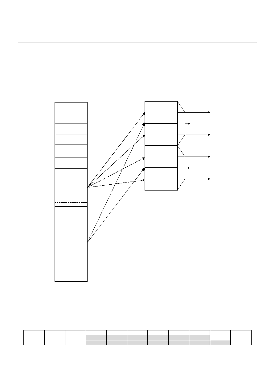
7.1 Memory map
ST2064 builds in 64K bytes ROM and 2K bytes RAM. The internal ROM can be used as data memory or program memory. PRR is
the Program ROM Bank Register and DRR is the Data ROM Bank Register. The logical program ROM address is from $4000 to
$7FFF(16K bytes), and $8000 to $FFFF (32K bytes) is for logical data ROM address.
.
Control Register
Reserved
0000
003F
0040
007F
SRAM
0080
0FFF
LCD RAM
1000
10AF
10B0
Reserved
3FFF
4000
Program Memory
(PRR)
16K bytes
7FFF
8000
Data Memory
(DRR)
32K bytes
FFFF
000000~
003FFF
004000~
007FFF
DRR = 00H
PRR = 01H
PRR = 00H
008000~
00BFFF
00C000~
00FFFF
DRR = 01H
PRR = 03H
PRR = 02H
Interrupt Vector
7FEE
CPU Memory Mapping
Physical Memory Mapping
64K Bytes
Reserved
07FF
0800
7.2 ROM
7.2.1 Bank Description
Setting corresponding value to register PRR (program memory) or DRR (data memory) when user wants uses different memory
bank.
FIGURE 7-1 ROM Bank Selection Registers ($31~$32)
Address
Register
R/W Bit7 Bit6 Bit5 Bit4 Bit3 Bit2 Bit1 Bit0
PRR
$31 RW -
-
-
-
-
- PRR1
PRR0
DRR
$32 RW -
-
-
-
-
-
- DRR0
Sitronix ST2064
Ver 1.0
7/46
10/11/02
7.3 RAM
Internal static RAM is for control registers, data RAM, stack RAM and the LCD frame buffer.
7.3.1 Control Registers
Address Name R/W
Bit 7
Bit 6
Bit 5
Bit 4
Bit 3
Bit 2
Bit 1
Bit 0
Default
$000 PA
R/W
PA[7] PA[6] PA[5] PA[4] PA[3] PA[2] PA[1] PA[0] 1111
1111
$001 PB
R/W PB[7] PB[6] PB[5] PB[4] PB[3] PB[2] PB[1] PB[0] 1111
1111
$002 PC
R/W PC[7] PC[6] PC[5] PC[4] PC[3] PC[2] PC[1] PC[0] 1111
1111
$008 PCA R/W PCA[7] PCA[6] PCA[5] PCA[4] PCA[3] PCA[2] PCA[1] PCA[0] 0000
0000
$009 PCB R/W PCB[7] PCB[6] PCB[5] PCB[4] PCB[3] PCB[2] PCB[1] PCB[0] 0000
0000
$00A PCC R/W PCC[7] PCC[6] PCC[5] PCC[4] PCC[3] PCC[2] PCC[1] PCC[0] 0000
0000
$00F PMCR R/W PULL PDBN INTEG
-
-
-
-
-
100 - - - - -
$010 PSG0L R/W PSG0[7] PSG0[6] PSG0[5] PSG0[4] PSG0[3] PSG0[2] PSG0[1] PSG0[0] 0000
0000
$011 PSG0H R/W
-
-
-
-
PSG0[11] PSG0[10] PSG0[9] PSG0[8] - - - - 0000
$012 PSG1L R/W PSG1[7] PSG1[6] PSG1[5] PSG1[4] PSG1[3] PSG1[2] PSG1[1] PSG1[0] 0000
0000
$013 PSG1H R/W
-
-
-
-
PSG1[11] PSG1[10] PSG1[9] PSG1[8] - - - - 0000
$014 DAC R/W DAC[7] DAC[6] DAC[5] DAC[4] DAC[3] DAC[2] DAC[1] DAC[0] 0000
0000
W
-
PCK[2] PCK[1] PCK[0] PRBS C1EN C0EN DACE=0 -000
0000
$016 PSGC
W
-
PCK[2] PCK[1] PCK[0] DMD[1] DMD[0] INH DACE=1 -000
0000
$017 VOL R/W VOL1[3] VOL1[2] VOL1[1] VOL1[0] VOL0[3] VOL0[2] VOL0[1] VOL0[0] 0000
0000
$021 BTM R/W
-
-
-
-
BTM[3]
BTM[2]
BTM[1]
BTM[0]
- - - - 0000
R PRS[7] PRS[6] PRS[5] PRS[4] PRS[3] PRS[2] PRS[1] PRS[0] 0000
0000
$023 PRS
W SRES SENA SENT
-
-
-
-
-
000 - - - - -
$024 T0M R/W
-
- T0M[5]
T0M[4] -
T0M[2] T0M[1] T0M[0] -
-00
-000
$025 T0C R/W T0C[7] T0C[6] T0C[5] T0C[4] T0C[3] T0C[2] T0C[1] T0C[0] 0000
0000
$026 T1M R/W
-
-
-
T1M[4] T1M[3] T1M[2] T1M[1] T1M[0] -
-
-0
0000
$027 T1C R/W T1C[7] T1C[6] T1C[5] T1C[4] T1C[3] T1C[2] T1C[1] T1C[0] 0000
0000
$030 SYS R/W XSEL OSTP XSTP XBAK WSKP WAIT
- LVDET
0000
00
-0
$031 PRR R/W
-
-
-
-
-
-
PRR[1]
PRR[0]
- - - - - -00
$032 DRR R/W
-
-
-
-
-
-
-
DRR[0]
- - - - - - -0
$039 LSEL R/W
-
-
-
LSEL[4] LSEL[3]
LSEL[2] LSEL[1] LSEL[0] - - - 1 1111
$03A LCTL R/W LPWR BLANK REV SCAN CTR[3] CTR[2] CTR[1] CTR[0] 1000
0000
$03B LCK R/W DRV[3] DRV[2] DRV[1] DRV[0]
-
LCK[2] LCK[1] LCK[0] 1111
-000
$03C IREQ R/W
-
-
IRBT
IRPT
IRT1
IRT0
IRDAC
IRX
- - 00 0000
$03E IENA R/W
-
-
IEBT
IEPT
IET1
IET0
IEDAC
IEX
- - 00 0000
Note: 1. Undefined bytes and bits should not be used.
2. Do not use bit modification instructions for write-only registers, such as RMBx, SMBx.
7.3.2 Data RAM ($0080~$07FF)
Data RAM are organized in 2K bytes from $0080~$07FF.
7.3.3 Stack RAM ($0100~$01FF)
Stack RAM is organized in 256 bytes. It provides for a maximum of 128-level subroutine stacks and can be used as data memory.
7.3.4 LCD Frame Buffer ($1000~$10AF)
LCD frame buffer is accessible by both read/write instructions and LCD controller. Note that this area can also be used as data
memory. Each pixel of LCD panel is directly mapped into this area. Refer to section 14.3 for the detail mapping.
Sitronix ST2064
Ver 1.0
8/46
10/11/02
8
8
.
.
I
I
N
N
T
T
E
E
R
R
R
R
U
U
P
P
T
T
S
S
8.1 Interrupt description
Brk
Instruction `BRK' will cause software interrupt when interrupt
disable flag (I) is cleared. Hardware will push `PC', `P '
Register to stack and set interrupt disable flag (I). Program
counter then will be loaded with the BRK vector from locations
$7FFE and $7FFF.
Reset
A positive transition of RESET pin will then cause an
initialization sequence to begin. After the system has been
operating, a low on this line at least of two clock cycles will
cease ST2064 activity. When a positive edge is detected, there
is an initialization sequence lasting six clock cycles. Then the
interrupt mask flag is set, the decimal mode is cleared and the
program counter will loaded with the restart vector from
locations $7FFC (low byte) and $7FFD (high byte). This is the
start location for program control. This input should be high in
normal operation.
INTX Interrupt
The IRX (INTX interrupt request) flag will be set while INTX
edge signal occurs. The INTX interrupt will be active once IEX
(INTX interrupt enable) is set, and interrupt mask flag is
cleared. Hardware will push `PC', `P ' Register to stack and set
interrupt mask flag (I). Program counter will be loaded with the
INTX vector from locations $7FF8 and $7FF9.
DAC Interrupt
The IRDAC (DAC interrupt request) flag will be set while reload
signal of DAC occurs. Then the DAC interrupt will be executed
when IEDAC (DAC interrupt enable) is set, and interrupt mask
flag is cleared. Hardware will push `PC', `P ' Register to stack
and set interrupt mask flag (I). Program counter will be loaded
with the DAC vector from locations $7FF6 and $7FF7.
T0 Interrupt
The IRT0 (TIMER0 interrupt request) flag will be set while T0
overflows. With IET0 (TIMER0 interrupt enable) being set, the
T0 interrupt will execute, and interrupt mask flag will be cleared.
Hardware will push `PC', `P ' Register to stack and set
interrupt mask flag (I). Program counter will be loaded with the
T0 vector from locations $7FF4 and $7FF5.
T1 Interrupt
The IRT1 (TIMER1 interrupt request) flag will be set while T1
overflows. With IET1 (TIMER1 interrupt enable) being set, the
T1 interrupt will execute, and interrupt mask flag will be cleared.
Hardware will push `PC', `P ' Register to stack and set
interrupt mask flag (I). Program counter will be loaded with the
T1 vector from locations $7FF2 and $7FF3.
PT Interrupt
The IRPT (Port-A interrupt request) flag will be set while Port-A
transition signal occurs. With IEPT (PT interrupt enable) being
set, the PT interrupt will be execute, and interrupt mask flag will
be cleared. Hardware will push `PC', `P ' Register to stack and
set interrupt mask flag (I). Program counter will be loaded with
the PT vector from locations $7FF0 and $7FF1.
BT Interrupt
The IRBT (Base timer interrupt request) flag will be set when
Base Timer overflows. The BT interrupt will be executed once
the IEBT (BT interrupt enable) is set and the interrupt mask flag
is cleared. Hardware will push `PC', `P ' Register to stack and
set interrupt mask flag (I). Program counter will be loaded with
the BT vector from locations $7FEE and $7FEF.
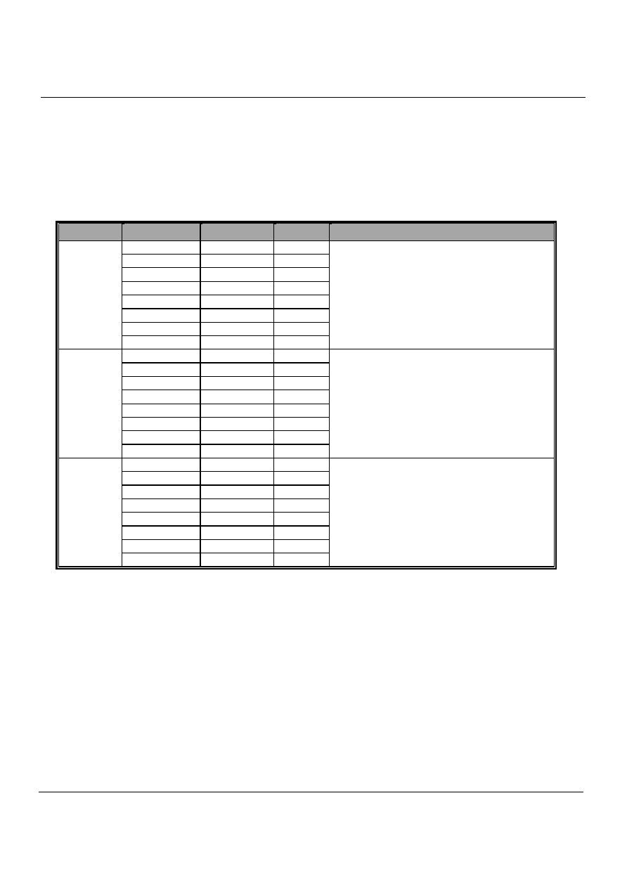
All interrupt vectors are listed in TABLE 8-1.
TABLE 8-1 Interrupt Vectors
Name Signal Vector
address
Priority
Comment
BRK
Internal
$7FFF,$7FFE
8
Software BRK operation vector
RESET External
$7FFD,$7FFC
1
Reset
vector
-
-
$7FFB,$7FFA
-
Reserved
INTX External $7FF9,$7FF8 2
PA0
edge
interrupt
DAC
Internal
$7FF7,$7FF6
3
Reload DAC data interrupt
T0 INT/EXT $7FF5,$7FF4 4
Timer0
interrupt
T1 INT/EXT $7FF3,$7FF2 5
Timer1
interrupt
PT External $7FF1,$7FF0 6
Port-A
transition
interrupt
BT
Internal
$7FEF,$7FEE
7
Base Timer interrupt
Sitronix ST2064
Ver 1.0
9/46
10/11/02
8.2 Interrupt Request Flag
Interrupt request flag can be cleared by two methods. One is to
write "0" to IREQ, the other is to initiate the interrupt service
routine when interrupt occurs. Hardware will automatically clear
the Interrupt flag.
TABLE 8-2 Interrupt Request Register (IREQ)
Address Name
R/W
Bit 7
Bit 6
Bit 5
Bit 4
Bit 3
Bit 2
Bit 1
Bit 0
Default
$03C IREQ R/W
-
-
IRBT
IRPT
IRT1
IRT0
IRDAC
IRX
- - 00 0000
Bit 5: IRBT: Base Timer Interrupt Request bit
1 = Time base interrupt occurs
0 = Time base interrupt doesn't occur
Bit 2: IRT0: Timer0 Interrupt Request bit
1 = Timer0 overflow interrupt occurs
0 = Timer0 overflow interrupt doesn't occur
Bit 4: IRPT: Port-A Interrupt Request bit
1 = Port-A transition interrupt occurs
0 = Port-A transition interrupt doesn't occur
Bit 1: IRDAC: DAC reload Interrupt Request bit
1 = DAC time out interrupt occurs
0 = DAC time out interrupt doesn't occur
Bit 3: IRT1: Timer1 Interrupt Request bit
1 = Timer1 overflow interrupt occurs
0 = Timer1 overflow interrupt doesn't occur
Bit 0: IRX: INTX Interrupt Request bit
1 = INTX edge interrupt occurs
0 = INTX edge interrupt doesn't occur
TABLE 8-3 Interrupt Enable Register (IENA)
Address Name
R/W
Bit 7
Bit 6
Bit 5
Bit 4
Bit 3
Bit 2
Bit 1
Bit 0
Default
$03E IENA *R/W
-
-
IEBT
IEPT
IET1
IET0
IEDAC
IEX
- - 00 0000
Bit 5: IEBT: Base Timer Interrupt Enable bit
1 = Time base interrupt enable
0 = Time base interrupt disable
Bit 2: IET0: Timer0 Interrupt Enable bit
1 = Timer0 overflow interrupt enable
0 = Timer0 overflow interrupt disable
Bit 4: IEPT: Port-A Interrupt Enable bit
1 = Port-A transition interrupt enable
0 = Port-A transition interrupt disable
Bit 1: IEDAC: DAC reload Interrupt Enable bit
1 = DAC time out interrupt enable
0 = DAC time out interrupt disable
Bit 3: IET1: Timer1 Interrupt Enable bit
1 = Timer1 overflow interrupt enable
0 = Timer1 overflow interrupt disable
Bit 0: IEX: INTX Interrupt Enable bit
1 = INTX edge interrupt enable
0 = INTX edge interrupt disable
Sitronix ST2064
Ver 1.0
10/46
10/11/02
9
9
.
.
I
I
/
/
O
O
P
P
O
O
R
R
T
T
S
S
9.1 Description
ST2064 can supply total 24 GPIOs divided into three I/O ports,
Port-A, Port-B, and Port-C. Besides I/O function, Port-B/C can
also be used as LCD segment drives. For detail pin assignment,
please refer to TABLE 9-1
TABLE 9-1 I/O Description
PORT NAME
PAD NAME
PAD NUMBER PIN TYPE
FEATURE
PA0/INTX 8 I/O
PA1 9
I/O
PA2 10
I/O
PA3 11
I/O
PA4 12
I/O
PA5 13
I/O
PA6 14
I/O
Port-A
PA7 15
I/O
Programmable input/output pin
SEG40/PB0 79 I/O
SEG41/PB1 80 I/O
SEG42/PB2 81 I/O
SEG43/PB3 82 I/O
SEG44/PB4 83 I/O
SEG45/PB5 84 I/O
SEG46/PB6 85 I/O
Port-B
SEG47/PB7 86 I/O
Programmable input/output pin
SEG32/PC0 71 I/O
SEG33/PC1 72 I/O
SEG34/PC2 73 I/O
SEG35/PC3 74 I/O
SEG36/PC4 75 I/O
SEG37/PC5 76 I/O
SEG38/PC6 77 I/O
Port-C
SEG39/PC7 78 I/O
Programmable input/output pin

Sitronix ST2064
Ver 1.0
11/46
10/11/02
9.2 Port-A
9.2.1 Port-A Description
Port-A is a bit-programmable bi-direction I/O port, which is
controlled by PCA register. It also provides bit programmable
pull-up resistor for each input pin. Two interrupts can be
triggered by Port-A, de-bounced interrupt for keyboard scan
and edge sensitive interrupt (PA0 only) for external event.
TABLE 9-2 Summary Of Port-A Registers
Address Name
R/W
Bit 7
Bit 6
Bit 5
Bit 4
Bit 3
Bit 2
Bit 1
Bit 0
Default
$000 PA
R/W PA[7] PA[6] PA[5] PA[4] PA[3] PA[2] PA[1] PA[0] 1111
1111
$008 PCA R/W PCA[7] PCA[6] PCA[5] PCA[4] PCA[3] PCA[2] PCA[1] PCA[0] 0000
0000
$00F PMCR R/W PULL PDBN
INTEG -
-
-
-
-
100 - - - - -
$03C IREQ R/W
-
-
IRBT IRPT IRT1
IRT0
IRDAC
IRX
- - 00 0000
$03E IENA R/W
-
-
IEBT IEPT IET1
IET0
IEDAC
IEX
- - 00 0000
9.2.2 Port-A I/O Control
Direction of Port-A is controlled by PCA. Each bit of PCA
controls the direction of one single I/O of Port-A respectively,
with "1" for output mode, and "0" for input mode.
TABLE 9-3 Port-A Control Register (PCA)
Address Name
R/W
Bit 7
Bit 6
Bit 5
Bit 4
Bit 3
Bit 2
Bit 1
Bit 0
Default
$008 PCA R/W PCA[7] PCA[6] PCA[5] PCA[4] PCA[3] PCA[2] PCA[1] PCA[0] 0000
0000
Bit 7~0: PCA[7~0] : Port-A directional bits
1 = Output mode
0 = Input mode
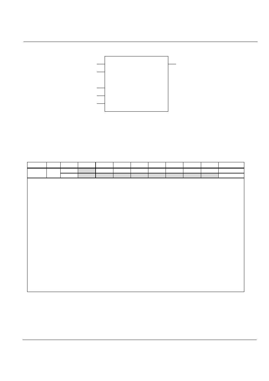
9.2.3 Port-A Pull-Up Option
Port-A contains PMOS transistors of pull-up resistor
controlled by software in bit-manner. In case of input
direction, on/off of the pull-up PMOS transistor is
controlled by the data wrote to data register, PA. "1" is
for enable and "0" is for disable. Above all, whole pull-up
control is by PULL bit of PMCR. Refer to FIGURE 9-1
for the block description.
VCC
PORT
DATA
REGISTER
( PDR )
PULL-UP
PMOS
PULL-UP
RD_INPUT
DATA INPUT
PORT
CONTROL
REGISTER
( PCR )
FIGURE 9-1 Port-A Block Diagram
TABLE 9-4 Port Function Control Register (PMCR)
Address Name
R/W
Bit 7
Bit 6
Bit 5
Bit 4
Bit 3
Bit 2
Bit 1
Bit 0
Default
$00F PMCR R/W PULL PDBN
INTEG -
-
-
-
-
100 - - - - -
Bit 7: PULL : Enable all pull-up function bit
1 = Enable pull-up function
0 = Disable pull-up function
Bit 6: PDBN : Enable Port-A interrupt de-bounce bit
1 = De-bounce for Port-A interrupt
0 = No de-bounce for Port-A interrupt
Bit 5: INTEG : INTX interrupt edge select bit
1 = Rising edge
0 = Falling edge
Sitronix ST2064
Ver 1.0
12/46
10/11/02
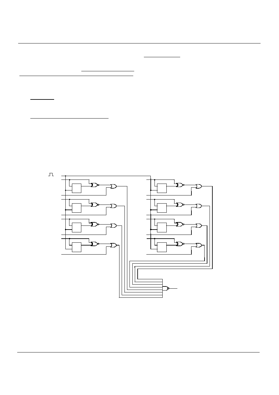
9.2.4 Port-A Interrupt
Port-A is suitable for the return line inputs of keyboard scan
because of the port transition interrupt function. Difference
between current value and the data kept previously of Port-A
will generate an interrupt request. The last state of Port-A must
be latched before transition, and this can be done by one read
instruction to Port-A. If both INTX and PT interrupts are enabled,
signal edge of PA0 may trigger PT interrupt as well as INTX.
Steps and program example are shown below. Also refer to
FIGURE 9-2 for the block diagram.
Operate Port-A interrupt steps:
1. Set input mode.
2. Read Port-A.
3. Clear interrupt request flag (IRPT).
4. Set interrupt enable flag (IEPT).
5. Clear CPU interrupt disable flag (I).
6. Read Port-A before `RTI' instruction in ISR.
Example:
.
.
STZ
<PCA
; Set input mode.
LDA #$FF
STA
<PA
; PA be PULL-UP.
LDA
<PA
; Keep last state.
RMB4 <IREQ
; Clear IRQ flag.
SMB4 <IENA
; Enable INT.
CLI
.
.
Interrupt subroutine
.
.
LDA <PA
; Keep last state.
RTI
NAND8
OR2
OR2
OR2
OR2
OR2
OR2
OR2
OR2
DFF
CK
D
Q
DFF
CK
D
Q
DFF
CK
D
Q
DFF
CK
D
Q
DFF
CK
D
Q
DFF
CK
D
Q
DFF
CK
D
Q
DFF
CK
D
Q
XNOR2
XNOR2
XNOR2
XNOR2
XNOR2
XNOR2
XNOR2
XNOR2
RDPA
PA[0]
PA[4]
PCA[0]
PCA[4]
PA[1]
PA[5]
PCA[1]
PCA[5]
PA[2]
PA[6]
PCA[2]
PCA[6]
PA[3]
PA[7]
PCA[3]
PCA[7]
PTIR
High Level Interrupt
FIGURE 9-2 Port Interrupt Logic Diagram

Sitronix ST2064
Ver 1.0
13/46
10/11/02
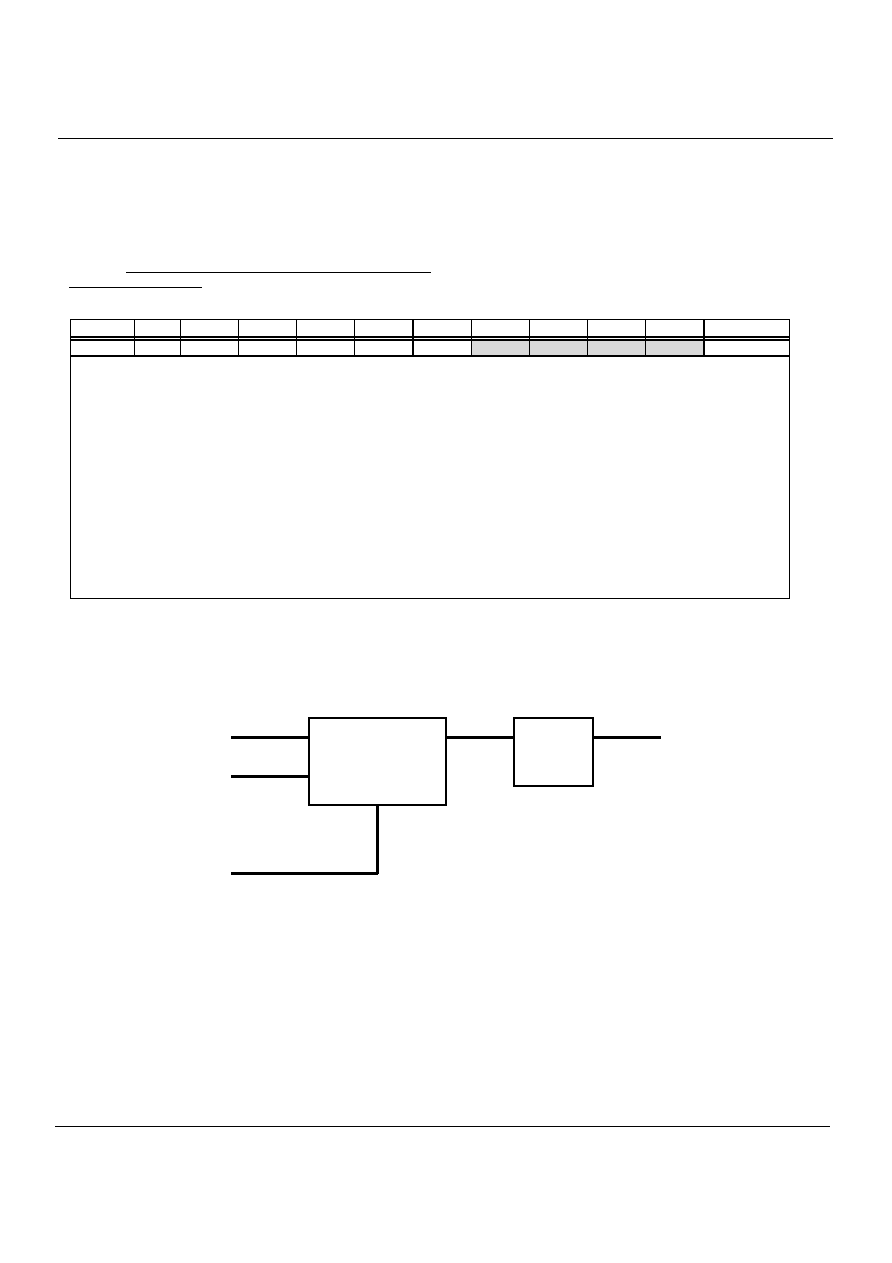
9.2.5 Port-A Interrupt De-bounce
ST2064 has hardware de-bounce block for Port-A interrupt. It
is enabled with "1" and disable with "0" of PDBN(PMCR[6]).
The de-bounce function is activated by Port-A transition. It
uses OSCX as the sampling clock. The de-bounce time is
OSCX x 512 cycles (about 16 ms). Data filtered by de-bounce
presents a stable state, then the interrupt can be issued.
TABLE 9-5 Port Function Control Register (PMCR)
Address Name
R/W
Bit 7
Bit 6
Bit 5
Bit 4
Bit 3
Bit 2
Bit 1
Bit 0
Default
$00F PMCR R/W
PULL PDBN INTEG
-
-
-
-
-
100 - - - - -
Bit 6: PDBN : Enable Port-A interrupt de-bounce bit
1 = De-bounce for Port-A interrupt
0 = No de-bounce for Port-A interrupt
9.2.6 PA0/INTX
PA0 plays another function of external edge-sensitive interrupt
source. Falling or rising edge is controlled by INTEG(PMCR[5]).
Please refer to FIGURE 9-3. If both INTX and PT interrupts are
enabled, signal edge of PA0 may trigger PT interrupt as well as
INTX. Steps and program example are shown below.
Steps for INTX interrupt operation:
1. Set PA0 to input mode. (PCA[0])
2. Select edge level. (INTEG)
3. Clear INTX interrupt request flag. (IRX)
4. Set INTX interrupt enable bits. (IEX)
5. Clear CPU interrupt mask flag (I).
Example:
.
.
RMB0 <PCA
; Set input mode.
SMB5 <PMCR
;
Rising
edge.
RMB0 <IREQ
; Clear IRQ flag.
SMB0 <IENA
; Enable INTX interrupt.
CLI
.
.
PMCR[5]
PA 0/INTX
Falling Edge Interrupt
FIGURE 9-3 INTX Logic Diagram

Sitronix ST2064
Ver 1.0
14/46
10/11/02
9.3 Port-B and Port-C
9.3.1 General Description
Port-B and Port-C are bit-programmable bi-direction I/O ports,
controlled by PCB and PCC registers. There is also bit
programmable pull-up resistor for each input pin. All of the 16
I/Os can change into LCD segment drives. Control register
LSEL specifies which of these I/Os are LCD drives.
TABLE 9-6 Summary of Port-B AND Port-C Registers
Address Name
R/W
Bit 7
Bit 6
Bit 5
Bit 4
Bit 3
Bit 2
Bit 1
Bit 0
Default
$001 PB
R/W PB[7] PB[6] PB[5] PB[4] PB[3] PB[2] PB[1] PB[0]
1111
1111
$002 PC
R/W PC[7] PC[6] PC[5] PC[4] PC[3] PC[2] PC[1] PC[0]
1111
1111
$009 PCB R/W PCB[7] PCB[6] PCB[5] PCB[4] PCB[3] PCB[2] PCB[1] PCB[0]
0000
0000
$00A PCC R/W PCC[7] PCC[6] PCC[5] PCC[4] PCC[3] PCC[2] PCC[1] PCC[0]
0000
0000
$00F PMCR R/W PULL PDBN
INTEG
-
-
-
-
-
100 - - - - -
$039 LSEL R/W
-
-
-
LSEL[4] LSEL[3] LSEL[2] LSEL[1] LSEL[0] - - - 1 1111
9.3.2 Input/Output Control
PCB/PCC controls the I/O direction of Port-B/C. Each bit of
PCB[7~0]/PCC[7~0] controls the direction of one single bit of
Port-B/C respectively, with "1" for output mode, and "0" for input
mode.
TABLE 9-7 PORT-B Control Register (PCB)
Address Name
R/W
Bit 7
Bit 6
Bit 5
Bit 4
Bit 3
Bit 2
Bit 1
Bit 0
Default
$009 PCB R/W PCB[7] PCB[6] PCB[5] PCB[4] PCB[3] PCB[2] PCB[1] PCB[0]
0000
0000
Bit 7~0: PCB[7~0] : Port-B directional bits
1 = Output mode
0 = Input mode
TABLE 9-8 PORT-C Control Register (PCC)
Address Name
R/W
Bit 7
Bit 6
Bit 5
Bit 4
Bit 3
Bit 2
Bit 1
Bit 0
Default
$00A PCC R/W PCC[7] PCC[6] PCC[5] PCC[4] PCC[3] PCC[2] PCC[1] PCC[0]
0000
0000
Bit 7~0: PCC[7~0] : Port-C directional bits
1 = Output mode
0 = Input mode

Sitronix ST2064
Ver 1.0
15/46
10/11/02
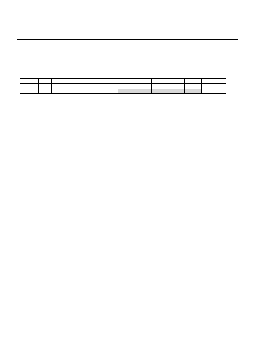
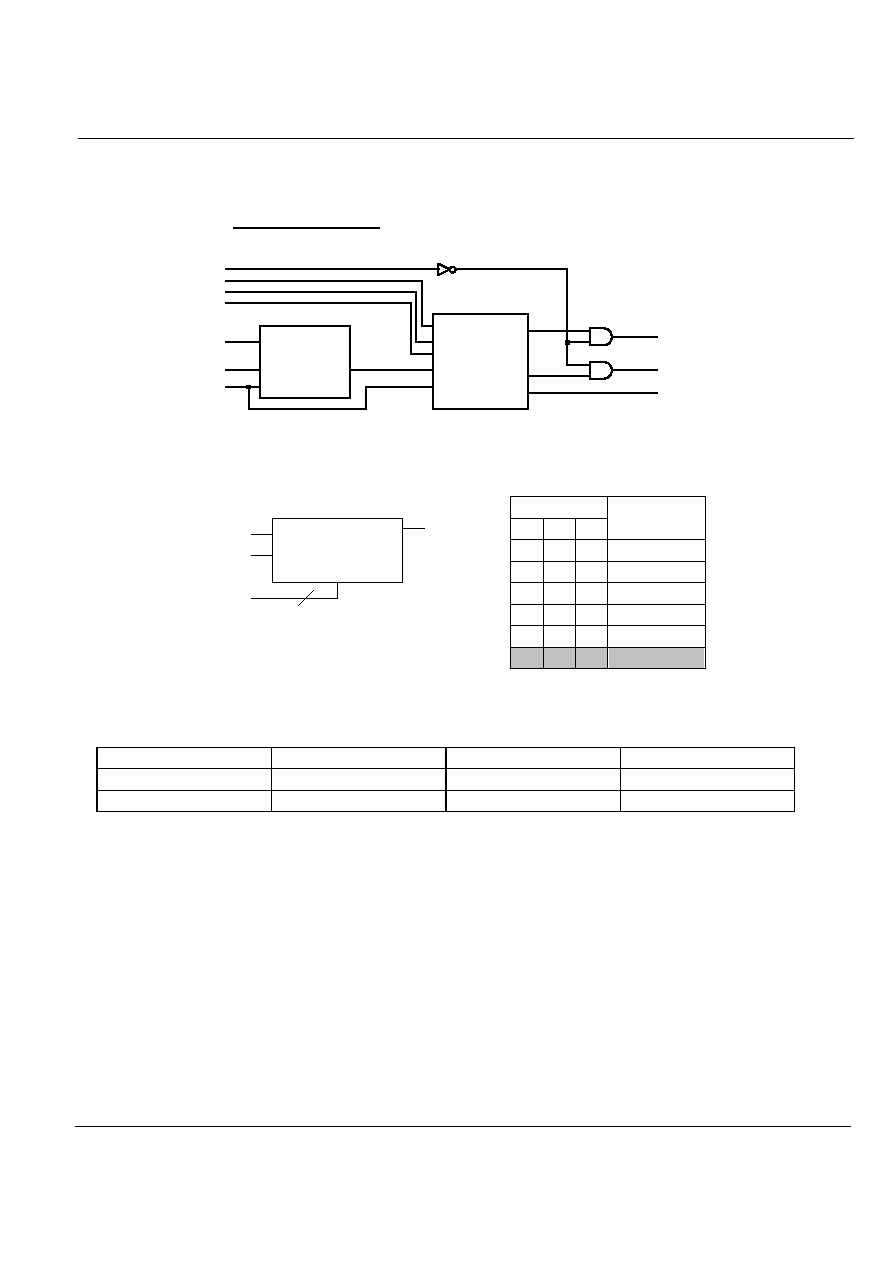
9.3.3 PORT-B and PORT-C PULL-UP OPTION
Port-B/C contains PMOS transistors of pull-up resistor
controlled by software in bit-manner. In case of input
direction, on/off of the pull-up PMOS transistor is
controlled by the data wrote to data register, PB/PC. "1"
is for enable and "0" is for disable. Above all, whole
pull-up control is by PULL bit of PMCR. Refer to
FIGURE 9-4 for the block description.
VCC
PORT
DATA
REGISTER
( PDR )
PULL-UP
PMOS
PULL-UP
RD_INPUT
DATA INPUT
PORT
CONTROL
REGISTER
( PCR )
FIGURE 9-4 Port-B and Port-C Block Diagram
TABLE 9-9 Port Control Register (PMCR)
Address Name R/W
Bit 7
Bit 6
Bit 5
Bit 4
Bit 3
Bit 2
Bit 1
Bit 0
Default
$00F PMCR R/W PULL PDBN
INTEG
-
-
-
-
-
100 - - - - -
Bit 7: PULL : Enable all pull-up functions bit
1 = Enable pull-up function
0 = Disable pull-up function
Sitronix ST2064
Ver 1.0
16/46
10/11/02
1
1
0
0
.
.
O
O
S
S
C
C
I
I
L
L
L
L
A
A
T
T
O
O
R
R
ST2064 has dual clock sources, OSC (RC) and OSCX
(32768Hz crystal). The system clock (SYSCK) can be
switched between OSC and OSCX, and is controlled by XSEL
(SYS[7]). When system clock is switched, the warm-up cycles
occur at the same time. Clock source being used is shown at
XSEL (read). Read and test XSEL to confirm SYSCK is
already switched over. Other blocks, such as LCD controller,
Timer1, Base Timer and PSG, can utilize these two clock
sources as well.
TABLE 10-1 System Control Register (SYS)
Address Name R/W
Bit 7
Bit 6
Bit 5
Bit 4
Bit 3
Bit 2
Bit 1
Bit 0
Default
$030 SYS R/W XSEL OSTP XSTP XBAK
WSKP
WAIT
-
LVDET 0000 00-0
Bit 7: XSEL : System clock (SYSCK) select (write) / confirm (read) bit
1 = OSCX
0 = OSC
Bit 6: OSTP : OSC stop control bit
1 = Disable OSC
0 = Enable OSC
Bit 5: XSTP : OSCX stop control bit
1 = Disable OSCX
0 = Enable OSCX
Bit 4: XBAK : OSCX driver heavy load bit
1 = OSCX normal load
0 = OSCX heavy load
Note:
1. XSEL (SYS[7]) shows which clock source is used for SYSCK when it is read.
2. System warm-up of 16 or 256 oscillation cycles occurs when system clock (SYSCK) is changed or power on reset.
/2
IN
OUT
MUX2
IN0
IN1
OUTPUT
SEL
OSC
SYSCK
OSCX
XSEL
Frequency divided by 2
FIGURE 10-1 System Clock Diagram

Sitronix ST2064
Ver 1.0
17/46
10/11/02
1
1
1
1
.
.
T
T
I
I
M
M
E
E
R
R
/
/
E
E
V
V
E
E
N
N
T
T
C
C
O
O
U
U
N
N
T
T
E
E
R
R
11.1 Prescaler
11.1.1 Function Description
The ST2064 has three timers, Base timer, Timer 0 and Timer 1,
and two prescalers PRES and PREW. There are two clock
sources, SYSCK and INTX, for PRES and one clock source,
OSCX, for PREW. Refer to FIGURE 11-1
TABLE 11-1 Summary of Timer Registers
Address Name R/W
Bit 7
Bit 6
Bit 5
Bit 4
Bit 3
Bit 2
Bit 1
Bit 0
Default
$021 BTM
W
-
-
-
- BTM[3]
BTM[2] BTM[1] BTM[0] - - - - 0000
R
PRS[7] PRS[6] PRS[5] PRS[4] PRS[3] PRS[2] PRS[1] PRS[0] 0000
0000
$023 PRS
W SRES
SENA
SENT -
-
-
-
-
000 - - - - -
$024 T0M R/W
-
- T0M[5]
T0M[4] -
T0M[2] T0M[1] T0M[0]
-
-00
-000
$025 T0C
R/W T0C[7] T0C[6] T0C[5] T0C[4] T0C[3] T0C[2] T0C[1] T0C[0] 0000
0000
$026 T1M R/W
-
-
-
T1M[4] T1M[3] T1M[2] T1M[1] T1M[0]
-
-
-0
0000
$027 T1C
R/W T1C[7] T1C[6] T1C[5] T1C[4] T1C[3] T1C[2] T1C[1] T1C[0] 0000
0000
$030 SYS R/W XSEL OSTP XSTP XBAK
WSKP
WAIT
-
-
0000 00- -
$03C IREQ R/W
-
- IRBT
IRPT IRT1 IRT0 IRDAC
IRX
-
-00
0000
$03E IENA R/W
-
- IEBT
IEPT IET1 IET0 IEDAC
IEX
-
-00
0000
SYSCK
INTX
SENT
O
SEL
MUX
SRES-PULSE
SENA
CK
ENABLE
CLEAR
OUTPUT
TCLK
PREW
OUTPUT
OSCX/256
OSCX/64
OSCX/16
OSCX/4
CK
RESET
OSCX
RESET
IN0
IN1
TCLK/2
PRES
BASE TIMER
TIMER 1
OSCX/128
OSCX/32
TIMER 0
TCLK/8
TCLK/32
TCLK/256
TCLK/2048
TCLK/8192
TCLK/32768
TCLK/65536
FIGURE 11-1 Structure Of Two Prescalers
Sitronix ST2064
Ver 1.0
18/46
10/11/02
11.1.2 PRES
The prescaler PRES is an 8-bits counter as shown in FIGURE
11-1. Which provides four clock sources for base timer and
timer1, and it is controlled by register PRS. The instruction read
toward PRS will bring out the content of PRES and the
Instruction write toward PRS will reset, enable or select clock
sources for PRES.
When user set external interrupt as the input of PRES for event
counter, combining PRES and Timer1 will get a 16bit-event
counter.
TABLE 11-2 Prescaler Control Register (PRS)
Address Name R/W
Bit 7
Bit 6
Bit 5
Bit 4
Bit 3
Bit 2
Bit 1
Bit 0
Default
R
PRS[7] PRS[6] PRS[5] PRS[4] PRS[3] PRS[2] PRS[1] PRS[0] 0000
0000
$023 PRS
W SRES
SENA
SENT -
-
-
-
-
000 - - - - -
READ
Bit 7~0: PRS[7~0] : The value of PRES counter
WRITE
Bit 7: SRES : Prescaler Reset bit
Write "1" to reset the prescaler (PRS[7~0])
Bit 6: SENA : Prescaler enable bit
0 = Disable prescaler counting
1 = Enable prescaler counting
Bit 5: SENT : Clock source(TCLK) selection for prescaller PRES
0 = Clock source from system clock "SYSCK"
1 = Clock source from external events "INTX"
11.1.3 PREW
The prescaler PREW is an 8-bits counter as shown in FIGURE
11-1. PREW provides four clocks source for base timer and
timer1. It stops counting only if OSCX stops or hardware reset
occurs.

Sitronix ST2064
Ver 1.0
19/46
10/11/02
11.2 Base timer
11.2.1 Function Description
Base timer is an 8-bit up counting timer. When it overflows from
$FF to $00, a timer interrupt request IRBT will be generated.
Please refer to FIGURE 11-2
IN0
IN1
IN2
IN3
SEL
PRES
BTM[2~0]
MUX4-1
PREW
IN0
IN1
IN2
IN3
SEL
BTM[1~0]
BTM[3]
IN0
IN1
SEL
MUX
8 Bit - UP Counter
CLOCK
IRBT
MUX 8-1
OSCX/256
OSCX/64
OSCX/16
OSCX/4
TCLK/256
TCLK/32
TCLK/8
TCLK/2
OUT
OUT
OUT
IN5
IN4
IN6
IN7
TCLK/2048
TCLK/8192
TCLK/32768
TCLK/65536
FIGURE 11-2 Structure Of Base Timer
11.2.2 Base Timer Clock Source Control
Several clock sources can be selected for Base Timer. Please
refer to TABLE 11-3
TABLE 11-3 Clock Sources Of Base Timer
*
SENA BTM[3] BTM[2] BTM[1] BTM[0] Base
Timer
source
clock
0
X
X
X
X STOP
1 0 0 0 0
TCLK
/
65536
1 0 0 0 1
TCLK
/
32768
1 0 0 1 0
TCLK
/
8192
1 0 0 1 1
TCLK
/
2048
1 0 1 0 0
TCLK
/
256
1 0 1 0 1
TCLK
/
32
1 0 1 1 0
TCLK
/
8
1 0 1 1 1
TCLK
/
2
X 1 0 0 0
OSCX
/
256
X 1 0 0 1
OSCX
/
64
X 1 0 1 0
OSCX
/
16
X 1 0 1 1
OSCX
/
4
Note: TCLK will stop when an `0' is written to SENA (PRS[6]).

Sitronix ST2064
Ver 1.0
20/46
10/11/02
11.3 Timer 0
11.3.1 Function Description
The Timer0 is an 8-bit up counter. It can be used as a timer or
an event counter. T0C($25) is a real time read/write counter.
When an overflow from $FF to $00, a timer interrupt request
IRT0 will
be generated. Timer0 will stop counting when system clock
stops. Please refer to FIGURE 11-3.
IN0
IN1
IN2
IN3
IN4
IN5
IN6
IN7
SEL
OUT
PRES
MUX 8-1
T0M[2~0]
TCLK/65536
TCLK/32768
TCLK/8192
TCLK/2048
TCLK/256
TCLK/32
TCLK/8
TCLK/2
T0M[4]
T0M[5]
Reload
Enable
CLOCK
8 Bit - UP Counter
OUT
IRT0
Auto
D
Q
CK
D Flip-Flop
SYSCK
FIGURE 11-3 Timer0 Structure
11.3.2 Timer0 Clock Source Control
Several clock sources can be chosen from for Timer0. It's very
important that Timer0 can keep counting as long as SYSCK
stays active. Refer to TABLE 11-4.
TABLE 11-4 Clock Sources Of Timer0
T 0M [2]
T 0M [1]
T 0M [0]
T 0 T i m er C lock S ource
0
0
0
T C LK /65536
0
0
1
T C LK /32768
0
1
0
T C LK /8192
0
1
1
T C LK /2048
1
0
0
T C LK /256
1
0
1
T C LK /32
1
1
0
T C LK /8
1
1
1
T C LK /2
T0M[4] : Control automatic reload operation
0 : No auto reload
1 : Auto reload
T0M[5] : Control Timer 0 enable/disable
0 : Disable counting
1 : Enable counting
SENA : Prescaler enable bit
0 : TCLK stop
1 : TCLK counting
TABLE 11-5 Timer0 Register (T0C)
Address Name R/W
Bit 7
Bit 6
Bit 5
Bit 4
Bit 3
Bit 2
Bit 1
Bit 0
Default
$025 T0C
R/W T0C[7] T0C[6] T0C[5] T0C[4] T0C[3] T0C[2] T0C[1] T0C[0] 0000
0000
Bit 7-0: T0C[7-0] : Timer0 up counter register

Sitronix ST2064
Ver 1.0
21/46
10/11/02
11.4 Timer 1
The Timer1 is an 8-bit up counter. It used as timer/counter as program specified. The difference between base timer is that Timer1
will halt during CPU SBY, but base timer will not. It is shown in FIGURE 11-4.
IN4
IN5
IN6
IN7
SEL
PRES
T1M[2~0]
MUX4-1
PREW
IN0
IN1
IN2
IN3
SEL
T1M[1~0]
8 Bit - UP Counter
CLOCK
IRT1
MUX 8-1
OSCX/256
OSCX/128
OSCX/64
OSCX/32
TCLK/256
TCLK/32
TCLK/8
TCLK/2
OUT
OUT
IN0
IN1
OUT
SEL
D
CK
Q
D Flip-Flop
SYSCK
MUX
T1M[3]
Auto Reload
T1M[4]
IN0
IN1
IN2
IN3
TCLK/65536
TCLK/32768
TCLK/8192
TCLK/2048
FIGURE 11-4 Timer1 Structure
TABLE 11-6 Timer1 Register (T1C)
Address Name R/W
Bit 7
Bit 6
Bit 5
Bit 4
Bit 3
Bit 2
Bit 1
Bit 0
Default
$027 T1C
R/W T1C[7] T1C[6] T1C[5] T1C[4] T1C[3] T1C[2] T1C[1] T1C[0] 0000
0000
Bit 7-0: T1C[7-0] : Timer1 up counter register
TABLE 11-7 Clock Sources Of Timer1
T1M[3]
T1M[2]
T1M[1]
T1M[0]
T1 Timer Clock Source
0
0
0
0
TCLK/65536
0
0
0
1
TCLK/32768
0
0
1
0
TCLK/8192
0
0
1
1
TCLK/2048
0
1
0
0
TCLK/256
0
1
0
1
TCLK/32
0
1
1
0
TCLK/8
0
1
1
1
TCLK/2
1
0
0
0
OSCX/256
1
0
0
1
OSCX/128
1
0
1
0
OSCX/64
1
0
1
1
OSCX/32
T1M[4]: Control automatic reload operation
0: No auto reload
1: auto reload
SENA : Prescaler enable bit
0 : TCLK stop
1 : TCLK counting
Sitronix ST2064
Ver 1.0
22/46
10/11/02
1
1
2
2
.
.
P
P
S
S
G
G
12.1 Function description
The built-in dual channel Programmable Sound Generator
(PSG) is controlled by registers. Its flexibility makes it useful in
applications such as music synthesis, sound effects generation,
audible alarms and tone signaling. In order to generate sound
effects while allowing the processor to perform other tasks, the
PSG can continue to produce sound after the initial commands
have been given by the CPU. The structure of PSG was shown
in FIGURE 12-2 and the PSG clock source is shown in
FIGURE 12-1. ST2064 has three playing modes. First is that
both channel0 (CH0) and channel1 (CH1) output square type
tones. Second is CH0 outputs square tone, and CH1 outputs
noise. Third mode is PWM DAC mode. Sounds of two channels
are mixed into one signal and are outputted in the form of
digital waveform from two pins, PSGOB/PSGO. Therefore one
AC waveform can be performed.
RC
OSCX
PSGC[6~4]
IN0
IN1
Output
Select
PSG Selector
PSGCK
PSGC
SYSCK
PSGCK
SYSCK/2
SYSCK/4
SYSCK/8
SYSCK x 2
OSCX
B6 B5 B4
0
0
0
X
X
0
1
1
1
1
1
1
1
0
1
0
0
0
FIGURE 12-1 PSG Clock Source Control
Enable Output
Enable
LOAD
Output
MUX2
IN0
IN1
OUTPUT
SEL
MUX2
IN0
IN1
OUTPUT
SEL
MUX2
IN0
IN1
OUTPUT
SEL
MIXER
CH1
Output
Vol_CH1
DACE
C1TEN
C1Tone
C1out
DACE
PSGC[2]
C1NEN
C1Noise
PSGC[3]
PSGOB
C1out
VOL[1~0]
PSGO
BD
BDB
DACE
From DAC Generator
Channel 1 Tone
Channel 1 Noise
Preload Data Before First Count
FIGURE 12-2 PSG Block Diagram
Sitronix ST2064
Ver 1.0
23/46
10/11/02
TABLE 12-1 Summary Of PSG Registers
Address Name R/W
Bit 7
Bit 6
Bit 5
Bit 4
Bit 3
Bit 2
Bit 1
Bit 0
Default
$010 PSG0L W
PSG0[7] PSG0[6] PSG0[5] PSG0[4] PSG0[3] PSG0[2] PSG0[1] PSG0[0] 0000 0000
$011 PSG0H W
-
-
-
-
PSG0[11] PSG0[10] PSG0[9] PSG0[8] - - - - 0000
$012 PSG1L W
PSG1[7] PSG1[6] PSG1[5] PSG1[4] PSG1[3] PSG1[2] PSG1[1] PSG1[0] 0000 0000
$013 PSG1H W
-
-
-
-
PSG1[11] PSG1[10] PSG1[9] PSG1[8] - - - - 0000
W
-
PCK[2] PCK[1] PCK[0] PRBS C1EN C0EN DACE=0
-
000
0000
$016 PSGC
W
-
PCK[2] PCK[1] PCK[0] DMD[1]
DMD[0]
INH
DACE=1 - 000 0000
$017 VOL
W VOL1[3] VOL1[2] VOL1[1] VOL1[0] VOL0[3] VOL0[2] VOL0[1] VOL0[0] 0000 0000
TABLE 12-2 PSG Volume Control Register (VOL)
Address Name R/W
Bit 7
Bit 6
Bit 5
Bit 4
Bit 3
Bit 2
Bit 1
Bit 0
Default
$017 VOL
W
VOL1[3] VOL1[2] VOL1[1] VOL1[0] VOL0[3] VOL0[2] VOL0[1] VOL0[0] 0000 0000
Bit 3~0: VOL0[3~0] : PSG channel 0 volume control bit
0000 = No sound output
0001 = 1/16 volume (PSGCK must >= 320K Hz)
:
0100 = 4/16 volume
:
1000 = 8/16 volume
:
1111 = Maximum volume (PSGCK must >= 20K Hz)
Bit 7~4: VOL1[3~0] : PSG channel 1 volume control bit
0000 = No sound output
0001 = 1/16 volume (PSGCK must >= 320K Hz)
:
0100 = 4/16 volume
:
1000 = 8/16 volume
:
1111 = Maximum volume (PSGCK must >= 20K Hz)
Note: If single channel is enable, then PSG volume control can be double. (16
+ 16 = 32 level volume control)
12.2 Tone Generator
12.2.1 General Description
The tone frequency is decided by PSGCK and 12-bit
programmable divider (PSG[11~0]). Please refer to
FIGURE 12-3 and.FIGURE 12-4.
12 Bit Auto-reload Up Counter
Tone out
OUTPUT
PSG0[11~8]
PSG0[7~0]
LOAD
C0EN
PSGCK
C0[11~8]
C0[7~0]
Latch
Enable
Frequency of Channel 0 Tone = PSGCK/(1000H-PCH0[11~0])/2
CLOCK
Channel 0
FIGURE 12-3 Tone Generator Channel 0
Sitronix ST2064
Ver 1.0
24/46
10/11/02
12 Bit Auto-reload Up Counter
Tone out
OUTPUT
PSG1[11~8]
PSG1[7~0]
LOAD
C1EN
PSGCK
C1[11~8]
C1[7~0]
Latch
Enable
Frequency of Channel 1 Tone = PSGCK/(1000H-PCH1[11~0])/2
CLOCK
Channel 1
FIGURE 12-4 Tone Generator Channel 1
12.2.2 PSG Tone Programming
Tone or DAC function is defined by register DACE. Write to
C1EN will enable tone generator when PSG is in tone
function. Noise or tone function is selected by PRBS.
TABLE 12-3 PSG Control Register (PSGC)
Address Name R/W
Bit 7
Bit 6
Bit 5
Bit 4
Bit 3
Bit 2
Bit 1
Bit 0
Default
W
-
PCK[2] PCK[1] PCK[0] PRBS C1EN C0EN DACE=0
-
000
0000
$016 PSGC
W
-
PCK[2] PCK[1] PCK[0] DMD[1] DMD[0]
INH
DACE=1 - 000 0000
Bit 0: DACE : Tone(Noise) or DAC Generator selection bit
1 = PSG is used as the DAC generator
0 = PSG is used as the Tone (Noise) generator
Bit 1: C0EN : PSG channel 0 (Tone) enable bit
1 = PSG0 (Tone) enable
0 = PSG0 (Tone) disable
Bit 2: C1EN : PSG channel 1 (Tone or Noise) enable bit
1 = PSG1 (Tone or Noise) enable
0 = PSG1 (Tone or Noise) disable
Bit 3: PRBS : Tone or Noise generator selection bit
1 = Noise generator
0 = Tone generator
Bit 6~4: PCK[2~0] : clock source selection for PSG and DAC
000 = SYSCK
X01 = SYSCK / 2
X10 = SYSCK / 4
011 = SYSCK / 8
100 = SYSCK x 2
111 = OSCX

Sitronix ST2064
Ver 1.0
25/46
10/11/02
12.3 Noise Generator Control
12.3.1 General description
Noise generator is shown in FIGURE 12-5, which base
frequency is controlled by PSG1[5~0]
PSG1[5~0]
PSGCK
Noise Prescaler
C1N[5~0]
CLOCK
OUTPUT
NCK
CLOCK
OUTPUT
16-Stage White Noise Generator
Noise out
NCK Frequency = PSGCK/(40H-PCH1[5~0])
FIGURE 12-5 Noise Generator
12.3.2 Noise Generator Programming
DACE defines noise or DAC function. Writing a "1" to C1EN
will enable noise generator when PSG is in noise mode
12.4 PSG Applicaion Circuit
Sounds of two channels are modulated by PSGCK and
combine together into one AC signal. Then it outputs on
PSGOB and PSGO. Positive part of the AC signal is output
from PSGO while the negative part is from PSGOB.
PSGOB
ST2064
Buzzer
PSGO
FIGURE 12-6 PSG application circuit

Sitronix ST2064
Ver 1.0
26/46
10/11/02
1
1
3
3
.
.
P
P
W
W
M
M
D
D
A
A
C
C
13.1 Function description
A built-in PWM DAC is for analog sampling data or voice
signals. The structure of DAC is shown in TABLE 13-1.
There is an interrupt signal from DAC to CPU whenever
DAC data update is needed and the same signal will decide
the sampling rate of voice. In DAC mode, the frequency of
RC oscillator can't be less than 2M Hz.
TABLE 13-1 Summary Of DAC Registers
Address Name R/W Bit 7
Bit 6
Bit 5
Bit 4
Bit 3
Bit 2
Bit 1
Bit 0
Default
$012 PSG1L W PSG1[7] PSG1[6] PSG1[5] PSG1[4] PSG1[3] PSG1[2] PSG1[1] PSG1[0] 0 0 0 0 0 0 0 0
$013 PSG1H W
-
-
-
-
PSG1[11] PSG1[10] PSG1[9] PSG1[8] - - - - 0 0 0 0
$014 DAC W
DAC[7] DAC[6]
DAC[5]
DAC[4]
DAC[3]
DAC[2]
DAC[1] DAC[0] 0 0 0 0 0 0 0 0
W
-
PCK[2]
PCK[1]
PCK[0]
PRBS
C1EN
C0EN DACE=0 - 0 0 0 0 0 - 0
$016 PSGC
W
-
PCK[2]
PCK[1]
PCK[0] DMD[1]
DMD[0]
INH
DACE=1 - 0 0 0 0 0 0 0
TABLE 13-2 DAC Data Register (DAC)
Address Name R/W Bit 7
Bit 6
Bit 5
Bit 4
Bit 3
Bit 2
Bit 1
Bit 0
Default
$014 DAC
W DAC[7] DAC[6] DAC[5] DAC[4] DAC[3] DAC[2] DAC[1] DAC[0] 0000
0000
Bit 7~0: DAC[7~0] : DAC output data
Note: For Single-Pin Single Ended mode, the effective output resolution is 7 bit.
TABLE 13-3 DAC Control Register (PSGC)
Address Name R/W Bit 7
Bit 6
Bit 5
Bit 4
Bit 3
Bit 2
Bit 1
Bit 0
Default
W
-
PCK[2]
PCK[1]
PCK[0]
PRBS
C1EN
C0EN DACE=0 - 000 00-0
$016 PSGC
W
-
PCK[2] PCK[1] PCK[0] DMD[1] DMD[0] INH DACE=1
-
000
0000
Bit 0: DACE : PSG play as Tone (Noise) or DAC Generator selection bit
1 = PSG is used as DAC Generator
0 = PSG is used as Tone (Noise) Generator
Bit 1: INH : DAC output inhibit control bit
1 = DAC output inhibit
0 = DAC output enable
Bit 3~2: DMD[1~0] : DAC output mode selection
00 = Single-Pin mode : 7 bit resolution
01 = Two-Pin Two Ended mode : 8 bit resolution
10 = Reserved
11 = Two-Pin Push Pull mode : 8 bit resolution
Bit 6~4: PCK[2~0] : PSGCK selection for PSG and DAC
000 = SYSCK
X01 = SYSCK / 2
X10 = SYSCK / 4
011 = SYSCK / 8
100 = SYSCK x 2 (= frequency of RC oscillator)
111 = OSCX
Note: In DAC mode, PSGCK must select SYSCK x 2 (PCK[2~0]=100) under RC=2MHz.
Sitronix ST2064
Ver 1.0
27/46
10/11/02
13.2 Sample Rate Control
PSG1L and PSG1H control the sample rate. PSG1[11~6]
controls PWM repeat times (usually set=111100 for four
times of DAC reload) and PSG1[5~0] usually set `1'. The
input clock source is controlled by PCK[2~0]. The block
diagram is shown as the following:
Sample Rate Generator
CK_IN
Enable
Output
PSG1[11~0]
PWM Generator
DAC[7~0]
Enable
Fs
PO
POB
Reload_DAC
INH
DAC[7~0]
DMD[0]
DMD[1]
BD
PSG1[11~0]
PSGCK
Fs
BDB
DACE
Reload_DAC
DMD[0]
DMD[1]
FIGURE 13-1 DAC Diagram
RC
OSCX
PSGC[6~4]
IN0
IN1
Output
Select
PSG Selector
PSGCK
PSGC
SYSCK
PSGCK
SYSCK/2
SYSCK/4
SYSCK/8
SYSCK x 2
OSCX
B6 B5 B4
0
0
0
X
X
0
1
1
1
1
1
1
1
0
1
0
0
0
FIGURE 13-2 DAC Clock Source Control
TABLE 13-4 DAC Sample Rate Description (RC
OSC
= 2MHz)
DAC interrupt frequency
PWM frequency
PSGC b6, b5, b4
PSG1H, PSG1L
8K 32K 100
00001111, 00111111
6K 12K 100
00001111, 10111111

Sitronix ST2064
Ver 1.0
28/46
10/11/02
13.3 PWM DAC Mode Options
The PWM DAC generator has three modes, Single-pin
mode, Two-pin two-ended mode and Two-pin push pull
mode. They are depended on the application used. The
DAC mode is controlled by DMD[1~0]. (TABLE 13-3)
13.3.1 Single-Pin Mode (7-bit Accuracy)
Single-pin mode is designed for use with a single-transistor
amplifier. It has 7 bits of resolution. The duty cycle of the
PSGO is proportional to the output value. If the output value
is 0, the duty cycle is 50%. As the output value increases
from 0 to 63, the duty cycle goes from being high 50% of
the time up to 100% high. As the value goes from 0 to -64,
the duty cycle decreases from 50% high to 0%. PSGOB is
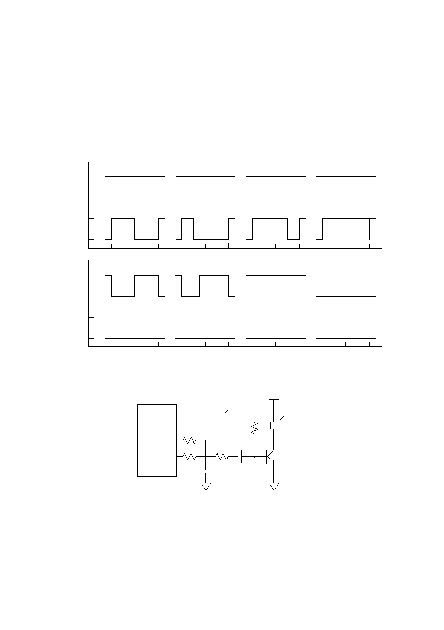
inverse of PSGO's waveform. Figure 13-3 shows the PSGO
waveforms.
DAC = 0
64
64
DAC = 32
DAC = -32
DAC = X
96
32
32
96
64+X
64-X
High
Low
PSGO
FIGURE 13-3 Single-Pin Mode Wave Form
PSGO
330 ohm
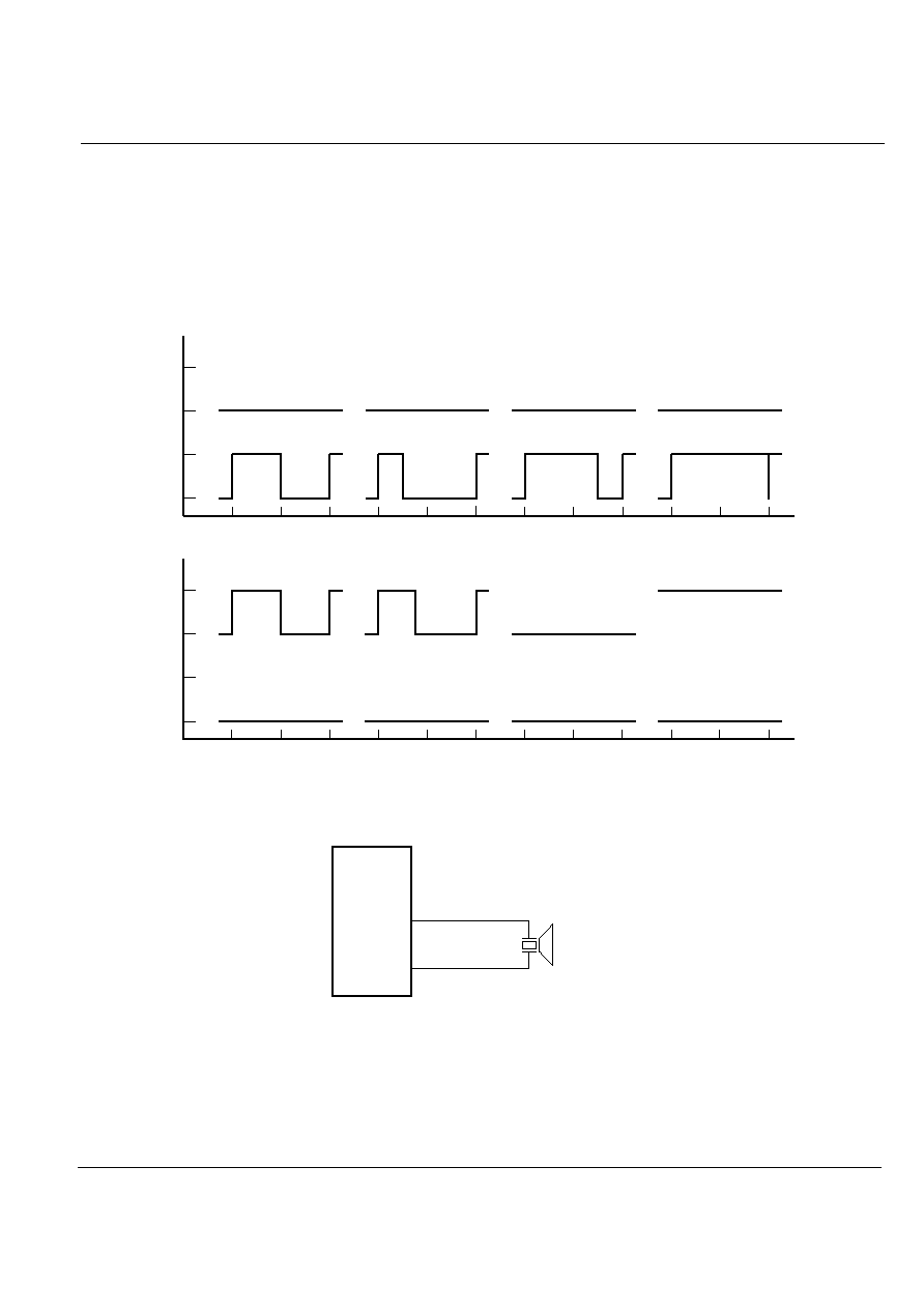
8050
ST2064
SPK
FIGURE 13-4 Single-Pin Mode Application Circuit
Sitronix ST2064
Ver 1.0
29/46
10/11/02
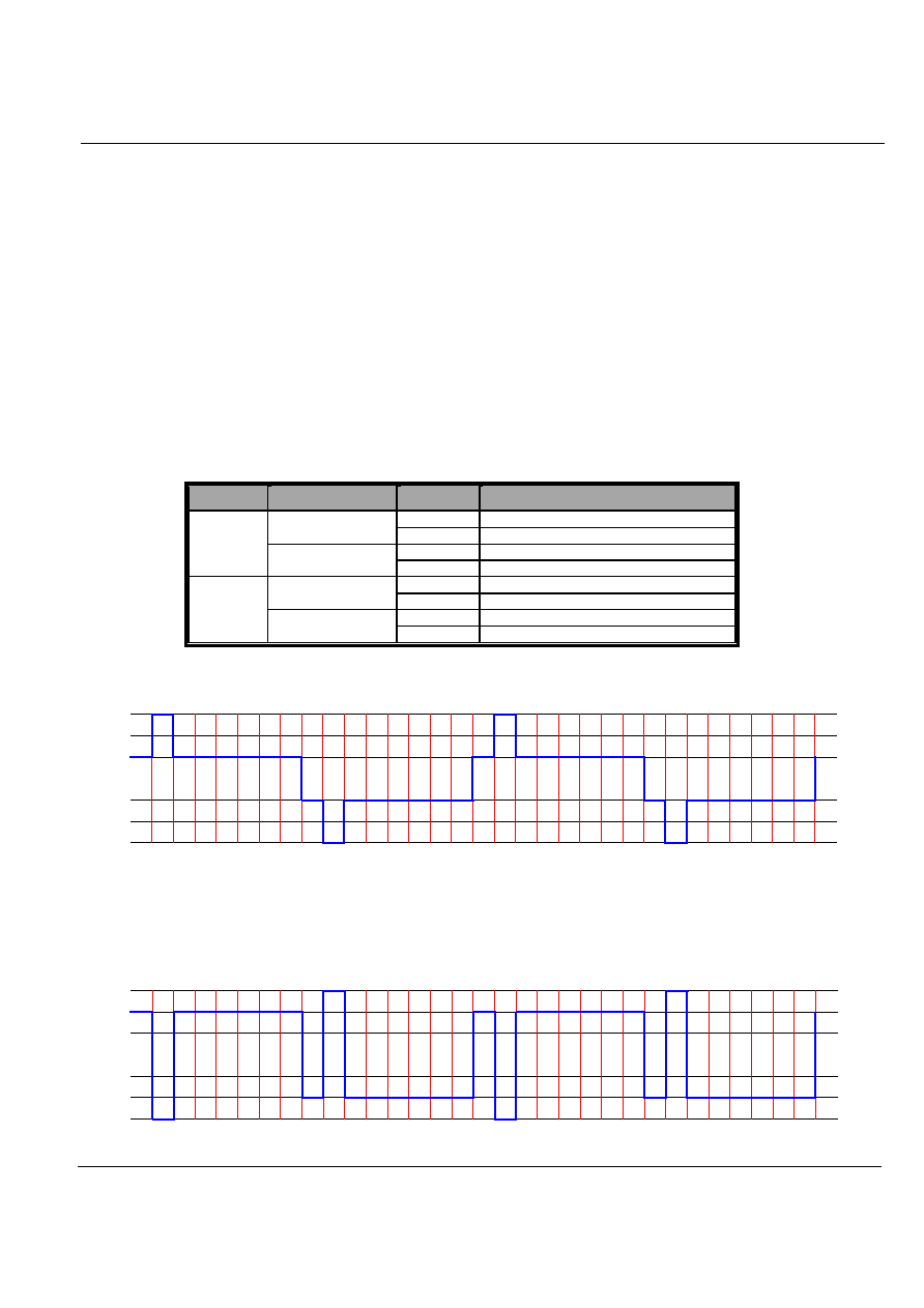
13.3.2 Two-Pin Two Ended Mode (8-bit Accuracy)
Two-Pin Two-Ended mode is designed for use with a single
transistor amplifier. It requires two pin that PSGO and
PSGOB. When the DAC value is positive, PSGO goes high
with a duty cycle proportional to the output value, while
PSGOB stays high. When the DAC value is negative,
PSGOB goes low with a duty cycle proportional to the
output value, while PSGO stays low. This mode offers a
resolution of 8 bits.
Figure 13-5 shows examples of DAC output waveforms with
different output values. Each pulse of the DAC is divided
into 128 segments per sample period. For a positive output
value x=0 to 127, PSGO goes high for X segments while
PSGOB stays high. For a negative output value x=0 to -127,
PSGOB goes low for |X| segments while PSGO stays low.
FIGURE 13-5 Two-Pin Two Ended Mode Wave-Form
PSGOB
680
8050
ST2064
PSGO
SPK
680
1K
0.1u
1u
2.2K
Output 1 : ON
0 : OFF
FIGURE 13-6 Two-Pin Two Ended Mode Application Circuit
High
Low
PSGOB
DAC = X
Where X=0 to 127
DAC = 96
High
Low
PSGO
X
128-X
DAC = 32
DAC = 127
127
1
96
32
32
96
High
Low
PSGOB
DAC = X
Where X=0 to -128
DAC = 0
High
Low
PSGO
|X|
128+X
DAC = -48
DAC = -128
48
80
Sitronix ST2064
Ver 1.0
30/46
10/11/02
13.3.3 Two-Pin Push Pull Mode (8-bit Accuracy)
Two-Pin Push Pull mode is designed for buzzer. It requires
two pin that PSGO and PSGOB. When the DAC value is 0,
both pins are low. When the DAC value is positive, PSGO
goes high with a duty cycle proportional to the output
value, while PSGOB stays low. When the DAC value is
negative, PSGOB goes high with a duty cycle proportional
to the output value, while PSGO stays low. This mode
offers a resolution of 8 bits.
Figure 13-7 shows examples of DAC output waveforms with
different output values. Each pulse of the DAC is divided
into 128 segments per sample period. For a positive output
value x=0 to 127, PSGO goes high for X segments while
PSGOB stays low. For a negative output value x=0 to -127,
PSGOB goes high for |X| segments while PSGO stays low.
FIGURE 13-7 Two-Pin Push Pull Mode Wave Form
PSGOB
ST2064
Buzzer
PSGO
FIGURE 13-8 Two-Pin Push Pull Mode Application Circuit
High
Low
PSGOB
DAC = X
Where X=0 to 127
DAC = 96
High
Low
PSGO
X
128-X
DAC = 32
DAC = 127
127
1
96
32
32
96
High
Low
PSG0
DAC = X
Where X=0 to -128
DAC = 0
High
Low
PSG1
|X|
128+X
DAC = -48
DAC = -128
48
80
PSGOB
PSGO
Sitronix ST2064
Ver 1.0
31/46
10/11/02
1
1
4
4
.
.
L
L
C
C
D
D
ST2064 is capable of driving one 1/16 duty, 1/5 bias LCD
panel of segment number from 32 to 48 (up to 768 dots).
LCD block includes display frame buffer ($1000~ $10AF)
for storing display data, 16 common and 32 segment
dedicated drives. The rest 16 segment drives are shared
with two I/O ports, Port-B/C. Data in frame buffer is
undefined after power on, so correct frame data should be
filled in before turn on display. One double DC-DC
converter is equipped for higher LCD voltage, and is
controlled by LPWR (LCTL[7]) for on/off. The LCD power
should be turned on before setting display on, and should
be turned off after setting display off. Both SYSCK and
OSCX can be chose as LCD clock source, therefore the
display can still works after power down. There are two
frame rate options, 64Hz and 85Hz, for each different clock
sources. In case of 64Hz frame rate, 8-level driving strength
and 12-level contrast are adjustable by software for
different panel size and LC voltage.
14.1 LCD Waveform
LCD driving waveform is based on the display data and the
alternation signal, which toggles every one frame. The
related output voltage levels are shown below. Figure 14-1
shows the common and segment waveforms for one frame.
TABLE 14-1 Driver Output Levels
Driver
Mode
Alternation
Display data output level
H VP
Selected
L V5
(GND)
H V1
Common
Non-selected
L V4
H VP
Selected
L V5
(GND)
H V2
Segment
Non-selected
L V3
VP
V2
V1
V3
V5
V4
FIGURE 14-1 LCD Segment Waveform
VP
V2
V1
V3
V5
V4
FIGURE 14-2 LCD Common Waveform

Sitronix ST2064
Ver 1.0
32/46
10/11/02
14.2 LCD Control Register
TABLE 14-2 LCD Segment Number Selection Register (LSEL)
Address Name R/W
Bit 7
Bit 6
Bit 5
Bit 4
Bit 3
Bit 2
Bit 1
Bit 0
Default
$039 LSEL R/W
-
-
-
LSEL[4] LSEL[3] LSEL[2] LSEL[1] LSEL[0] -
-
-1
1111
Bit 4~0: LSEL[4:0] : LCD segment number selection
Pad Definition
LSEL[4:0] PAD
71
PAD
72
PAD
73
PAD
74
PAD
75
PAD
76
PAD
77
PAD
78
PAD
79
PAD
80
PAD
81
PAD
82
PAD
83
PAD
84
PAD
85
PAD
86
0 xxxx
PC0
PC1
PC2
PC3
PC4
PC5
PC6
PC7
PB0
PB1
PB2
PB3
PB4
PB5
PB6
PB7
1 0000 SEG32 PC1
PC2
PC3
PC4
PC5
PC6
PC7
PB0
PB1
PB2
PB3
PB4
PB5
PB6
PB7
1 0001 SEG32 SEG33 PC2
PC3
PC4
PC5
PC6
PC7
PB0
PB1
PB2
PB3
PB4
PB5
PB6
PB7
1 0010 SEG32 SEG33 SEG34 PC3
PC4
PC5
PC6
PC7
PB0
PB1
PB2
PB3
PB4
PB5
PB6
PB7
1 0011 SEG32 SEG33 SEG34 SEG35 PC4
PC5
PC6
PC7
PB0
PB1
PB2
PB3
PB4
PB5
PB6
PB7
1 0100 SEG32 SEG33 SEG34 SEG35 SEG36 PC5
PC6
PC7
PB0
PB1
PB2
PB3
PB4
PB5
PB6
PB7
1 0101 SEG32 SEG33 SEG34 SEG35 SEG36 SEG37 PC6
PC7
PB0
PB1
PB2
PB3
PB4
PB5
PB6
PB7
1 0110 SEG32 SEG33 SEG34 SEG35 SEG36 SEG37 SEG38 PC7
PB0
PB1
PB2
PB3
PB4
PB5
PB6
PB7
1 0111
SEG32 SEG33 SEG34 SEG35 SEG36 SEG37 SEG38 SEG39 PB0
PB1
PB2
PB3
PB4
PB5
PB6
PB7
1 1000 SEG32 SEG33 SEG34 SEG35 SEG36 SEG37 SEG38 SEG39 SEG40 PB1
PB2
PB3
PB4
PB5
PB6
PB7
1 1001 SEG32 SEG33 SEG34 SEG35 SEG36 SEG37 SEG38 SEG39 SEG40 SEG41 PB2
PB3
PB4
PB5
PB6
PB7
1 1010 SEG32 SEG33 SEG34 SEG35 SEG36 SEG37 SEG38 SEG39 SEG40 SEG41 SEG42 PB3
PB4
PB5
PB6
PB7
1 1011
SEG32 SEG33 SEG34 SEG35 SEG36 SEG37 SEG38 SEG39 SEG40 SEG41 SEG42 SEG43 PB4
PB5
PB6
PB7
1 1100
SEG32 SEG33 SEG34 SEG35 SEG36 SEG37 SEG38 SEG39 SEG40 SEG41 SEG42 SEG43 SEG44 PB5
PB6
PB7
1 1101
SEG32 SEG33 SEG34 SEG35 SEG36 SEG37 SEG38 SEG39 SEG40 SEG41 SEG42 SEG43 SEG45 SEG45 PB6
PB7
1 1110
SEG32 SEG33 SEG34 SEG35 SEG36 SEG37 SEG38 SEG39 SEG40 SEG41 SEG42 SEG43 SEG45 SEG45 SEG46 PB7
1 1111
SEG32 SEG33 SEG34 SEG35 SEG36 SEG37 SEG38 SEG39 SEG40 SEG41 SEG42 SEG43 SEG45 SEG45 SEG46 SEG47
Sitronix ST2064
Ver 1.0
33/46
10/11/02
TABLE 14-3 LCD Control Register (LCTL)
Address Name R/W
Bit 7
Bit 6
Bit 5
Bit 4
Bit 3
Bit 2
Bit 1
Bit 0
Default
$03A LCTL R/W LPWR BLANK REV SCAN CTR[3] CTR[2] CTR[1] CTR[0] 1000
0000
Bit 7: LPWR : LCD power ON/OFF bit
1 = LCD power OFF
0 = LCD power ON
Bit 6: BLANK : LCD display ON/OFF bit
1 = Disable LCD display (Common line is still scanning)
0 = Enable LCD display
Bit 5: REV : LCD display reverse
1 = Reverse display
0 = Normal display
Bit 4: SCAN : LCD segment keyboard scan function
1 = Enable LCD keyboard awaking pulse in LCD waveforms
0 = Disable LCD keyboard awaking pulse
Bit 3~0: CTR[3~0] : LCD contrast control
Frame Rate = 64Hz
Frame Rate = 85Hz
00xx = contrast
level 12
0100 = contrast level 12 (maximum)
0101 = contrast level 11
0110 = contrast level 10
0111 = contrast
level 9
1000 = contrast level 8
1001 = contrast level 7
1010 = contrast level 6
1011 = contrast level 5
1100 = contrast level 4
1101 = contrast level 3
1110 = contrast
level 2
1111 =
contrast
level 1
(minimum)
0xxx = contrast
level 8
1000 = contrast level 8 (maximum)
1001 = contrast level 7
1010 = contrast level 6
1011 = contrast level 5
1100 = contrast level 4
1101 = contrast level 3
1110 = contrast
level 2
1111 =
contrast
level 1
(minimum)
TABLE 14-4 LCD Clock Source and Driving Strength Control Register
Address Name R/W
Bit 7
Bit 6
Bit 5
Bit 4
Bit 3
Bit 2
Bit 1
Bit 0
Default
$03B LCK
R/W DRV[3] DRV[2] DRV[1] DRV[0]
-
LCK[2] LCK[1] LCK[0] 1111
-000
Bit 7~3: DRV[3:0] : LCD driving strength control
Frame Rate = 64Hz
Frame Rate = 85Hz
0000 =
driving
level
16/16
(maximum)
0001 =
driving
level
15/16
0010 =
driving
level
14/16
:
:
:
1110 =
driving
level
3/16
1110 =
driving
level
2/16
1111
= driving level 1/16 (minimum)
00XX =
driving
level
12/12
0100 =
driving
level
12/12(maximum)
0101 =
driving
level
11/12
:
:
:
1101 =
driving
level
3/12
1110 =
driving
level
2/12
1111
= driving level 1/12 (minimum)
Bit 2~0: LCK[2:0] : LCD frame rate control
LCK[2:0]
Clock Source
Frame Rate
000 OSCX
(32768Hz) 64
Hz
001 OSCX
(32768Hz) 85
Hz
010 OSC
(2MHz) 64
Hz
011 OSC
(2MHz) 85
Hz
100 OSC
(4MHz) 64
Hz
101 OSC
(4MHz) 85
Hz
110 OSC
(8MHz) 64
Hz
111 OSC
(8MHz) 85
Hz

Sitronix ST2064
Ver 1.0
34/46
10/11/02
14.3 Keyboard-scan Function on LCD drives
VP
V2
V1
V3
V5
V4
FIGURE 14-3 LCD Segment Waveform (With Keyboard Awaking Pulses)
VP
V2
V1
V3
V5
V4
FIGURE 14-4 LCD Common Waveform (With Keyboard Awaking Pulses)
14.3.2 Keyboard-scan Function Example:
a. Keyboard : 64Keys (8x8)
b. Return Lines : Port-A
c. Scan Lines : Port-B/C
.
.
.
INITIAL_Port_And_LCD
SMB4 <LCTL
;;Enable Keyboard Awaking Waveform
LDA #000
11111B
;;Set all shared pins to be segments
STA <LSEL
STZ
<PCA
;;Set Port-A as Inputs for Return Line
LDA
#FFH
STA
<PA
;;Port-A
Pull-High
STA
<PCB
;;Set Port-B as Outputs for Scan Line
LDA
#10000000B
STA
<PMCR
;;Enable Pull up,Disable Debounce
LDA
#00010000B
STA
<IENA ;;Enable
Port-A
Interrupt
LDA
<PA
STZ
<IREQ
;;Reset Interrupt Request Register
.
.
CLI
.
Initial I/O
(Disable Debouncd)
CLI
Initial Interrupt/LCD
.
.
.
FIGURE 14-5 Initial Flow Chart

Sitronix ST2064
Ver 1.0
35/46
10/11/02
.
Interrupt-Subroutine
Port_ISR
PHA
PHX
LDA
#11111110B
;;Initial scanning value for Port-B
STA
<ScanValue
?Scan_PB
STA
<PB
RMB3
<LSEL
;;Change segments to be Port-B
nop
;;Wait for return line to be stable
nop
nop
LDA
<PA
SMB3
<LSEL
;;Change Port-B to be segments
JSR
Store-Key-Data ;;This subroutine should be defined by user
SEC
ROL
<Scanvalue
;;Shift scanning value left
LDA <ScanValue
BCS
?Scan_PB
;;Keep on scanning until ScanValue = FF
.
.
PLX
PLA
RTI
End of Scanning?
RTI
Read Port-A
Wait Port-A to be Stable
Turn ON Port-B
Output Scan Value on
Scan Lines
Turn OFF Port-B
Store Key Data
Yes
No
FIGURE 14-6 Port Interrupt Flow Chart

Sitronix ST2064
Ver 1.0
36/46
10/11/02
14.4 LCD Frame Buffer
Each pixel of LCD panel is directly mapped into LCD frame
buffer. If some segments are not used, the corresponding
RAM can still be accessed for data memory. Refer to
TABLE 14-5 for detail mapping.
TABLE 14-5 LCD Frame Buffer Memory Mapping
SEG0
SEG1
SEG2
SEG3
SEG4
SEG5
SEG47
Address 1000H 1001H 1002H 1003H 1004H 1005H
102FH
COM0
Bit7 Bit7 Bit7 Bit7 Bit7 Bit7
Bit7
COM1
Bit6 Bit6 Bit6 Bit6 Bit6 Bit6
Bit6
COM2
Bit5 Bit5 Bit5 Bit5 Bit5 Bit5
Bit5
COM3
Bit4 Bit4 Bit4 Bit4 Bit4 Bit4
Bit4
COM4
Bit3 Bit3 Bit3 Bit3 Bit3 Bit3
Bit3
COM5
Bit2 Bit2 Bit2 Bit2 Bit2 Bit2
Bit2
COM6
Bit1 Bit1 Bit1 Bit1 Bit1 Bit1
Bit1
COM7
Bit0 Bit0 Bit0 Bit0 Bit0 Bit0
......
......
......
Bit0
Address 1080H 1081H 1082H 1083H 1084H 1085H
10AFH
COM8
Bit7 Bit7 Bit7 Bit7 Bit7 Bit7
Bit7
COM9
Bit6 Bit6 Bit6 Bit6 Bit6 Bit6
Bit6
COM10
Bit5 Bit5 Bit5 Bit5 Bit5 Bit5
Bit5
COM11
Bit4 Bit4 Bit4 Bit4 Bit4 Bit4
Bit4
COM12
Bit3 Bit3 Bit3 Bit3 Bit3 Bit3
Bit3
COM13
Bit2 Bit2 Bit2 Bit2 Bit2 Bit2
Bit2
COM14
Bit1 Bit1 Bit1 Bit1 Bit1 Bit1
Bit1
COM15
Bit0 Bit0 Bit0 Bit0 Bit0 Bit0
......
......
......
Bit0
Note: Undefined RAM area, $1030~$107F and $10B0~$10FF, is not accessible.

Sitronix ST2064
Ver 1.0
37/46
10/11/02
1
1
5
5
.
.
P
P
O
O
W
W
E
E
R
R
D
D
O
O
W
W
N
N
M
M
O
O
D
D
E
E
S
S
ST2064 has three power down modes: WAI-0, WAI-1 and
STP. The instruction WAI will enable either WAI-0 or WAI-1,
which is controlled by WAIT(SYS[2]). And the instruction
STP will enable STP mode in the same manner. WAI-0 and
WAI-1 modes can be waked up by interrupt. However, STP
mode can only be waked up by hardware reset.
TABLE 15-1 System Control Register (SYS)
Address Name R/W
Bit 7
Bit 6
Bit 5
Bit 4
Bit 3
Bit 2
Bit 1
Bit 0
Default
$030 SYS
R/W XSEL OSTP XSTP XBAK WSKP WAIT -
LVDET 0000
00-0
Bit 3: WSKP : System warm-up control bit
1 = Warm-up to 16 oscillation cycles
0 = Warm-up to 256 oscillation cycles
Bit 2: WAIT : WAI-0 / WAI-1mode select bit
1 = WAI instruction causes the chip to enter WAI-1 mode
0 = WAI instruction causes the chip to enter WAI-0 mode
15.1 WAI-0 Mode:
If WAIT is cleared, WAI instruction makes MCU enter WAI-0
mode. In the mean time, the oscillator, interrupts,
timer/counter, and PSG are still working. On the other hand
CPU and the related instruction execution stop. All registers,
RAM, and I/O pins will retain the same states as those
before the MCU entered power down mode. WAI-0 mode
can be waked up by reset or interrupt request even If user
sets interrupt disable flag I. In that case MCU will be waked
up but not entering interrupt service routine. If interrupt
disable flag is cleared (I='0'), the corresponding interrupt
vector will be fetched and the service routine will be
executed. The sample program is shown below:
LDA #$00
STA <SYS
WAI
; WAI 0 mode
15.2 WAI-1 Mode:
If WAIT is set, WAI instruction makes MCU enter WAI-1
mode. In this mode, CPU stops, but the PSG, timer/counter
keep running if their clock sources are from OSCX. The
wake-up procedure is the same as for WAI-0. The
difference is that the warm-up cycles occurs when waking
from WAI-1. Sample program is shown as following:
LDA #$04
STA <SYS
WAI
; WAI 1 mode
15.3 STP Mode:
STP instruction will force MCU to enter stop mode. In this
mode, MCU stops, but PSG, timer/counter won't stop if the
clock source is from OSCX. In power-down mode, MCU
can only be waked up by hardware reset, and the warm-up
cycles occurs at the same time.

Sitronix ST2064
Ver 1.0
38/46
10/11/02
FIGURE 15-1 Status Under Power Dowm Modes
SYSCK source is OSC:
Mode Timer0,1 SYSCK OSC OSCX
Base
Timer
RAM REG. LCD I/O Wake-up
condition
WAI-0
Retain
Reset, Any interrupt
WAI-1
Stop
Stop
Stop Retain Reset,
Any
interrupt
STP Stop
Stop Stop
Retain
Reset
SYSCK source is OSCX:
Mode Timer0,1 SYSCK OSC OSCX
Base
Timer
RAM REG. LCD I/O Wake-up
condition
WAI-0
Retain
Reset, Any interrupt
WAI-1
Stop
Stop
Retain
Reset, Any interrupt
STP Stop
Stop
Retain
Reset
Sitronix ST2064
Ver 1.0
39/46
10/11/02
1
1
6
6
.
.
L
L
O
O
W
W
V
V
O
O
L
L
T
T
A
A
G
G
E
E
D
D
E
E
T
T
E
E
C
C
T
T
O
O
R
R
ST2064 has a built-in low voltage detector for power
management. When LVDET is set, detector circuit is
enabled and the detection result will be outputted at the
same bit after 3
�s. Using read instruction twice can get
this result: first read will enable initial stableness control.
Second read equal '1' represents 'low voltage'. Once low
voltage detector is enabled, it keeps on consuming power.
So it is important that remember to write "0" to LVDET to
disable the detector after detection is completed. One
sample program is shown below:
Start:
SMB0 <SYS
;
enable
detector
:
Wait 3
�
�
�
�s
:
CLC
BBR0 <SYS,$+3
BBR0 <SYS,Normal_Voltage
Low_Voltage:
SEC
Normal_Voltage:
RMB0 <SYS
;
disable
detector
TABLE 16-1 System Control Register (SYS)
Address Name R/W
Bit 7
Bit 6
Bit 5
Bit 4
Bit 3
Bit 2
Bit 1
Bit 0
Default
$030 SYS R/W
XSEL
OSTP
XSTP
XBAK
WSKP
WAIT
- LVDET
0000
00-0
Bit 0: LVDET : Low voltage detect
1 = Enable detector (write) / Low voltage (read)
0 = Disable detector (write) / Normal voltage (read)
Sitronix ST2064
Ver 1.0
40/46
10/11/02
1
1
7
7
.
.
E
E
L
L
E
E
C
C
T
T
R
R
I
I
C
C
A
A
L
L
C
C
H
H
A
A
R
R
A
A
C
C
T
T
E
E
R
R
I
I
S
S
T
T
I
I
C
C
S
S
DC Supply Voltage ---------------------------- -0.3V to +4.5V
Operating Ambient Temperature ---------- -10
�C to +60�C
Storage Temperature ------------------------ -10
�C to +125�C
17.1 DC Electrical Characteristics
Standard operation conditions: VCC
= 3.0V, GND = 0V, T
A
= 25
�C, OSC = 2M Hz, unless otherwise specified
Parameter
Symbol
Min. Typ. Max. Unit
Condition
5.5 Logic
Operating Voltage
VCC
2.4
3.4
V Built-in double DC-DC voltage converter for LCD
driver:
Operating Current
I
OP
749
599
�A
All I/O ports are input and pull-up, LCD driving
strength is maximum.
Standby Current
I
SB0
1.3
�A
All I/O ports are input and pull-up, OSCX on, LCD off
(WAIT1/STOP mode)
Standby Current
I
SB1
60.3
�A
All I/O ports are input and pull-up, OSCX on, LCD off
(WAIT0 mode)
LCD consumption
I
LCD
21
�A
LCD Clock source=OSCX Driving strength=1/16
Condition: WAIT1 mode.
LCD consumption
I
LCD
125
�A
LCD Clock source=OSCX Driving strength=16/16
Condition: WAIT1 mode.
Input High Voltage
V
IH
0.7Vcc
Vcc+0.3
V
PORT A, PORT B, PORT C
0.85Vcc
V
RESET , INT
Input Low Voltage
V
IL
GND-0.3
0.3Vcc
V
PORT A, PORT B, PORT C
0.15Vccc
V
RESET , INT
Pull-up resistance
R
I
H
150
K
PORTA (Voltage difference=0.9V)
Pull-up resistance
R
I
H
190
K
PORTB, PORT C (Voltage difference=0.9V)
Output high voltage
V
OH
1
0.7Vcc
V PORTA
(IOH=-3.5mA)
Output high voltage
V
OH
1
0.7Vcc
V PORTB, PORTC (IOH=-2.5mA)
Output low voltage
V
OL
1
0.3Vcc
V
PORTA
(IOL=7.5mA)
Output low voltage
V
OL
1
0.3Vcc
V
PORTB,
PORT
C
(IOL=4.5mA)
Output high voltage
V
OH
2
0.7Vcc
V PB0/1 as PSG/DAC, IOH = -25mA.
Output low voltage
V
OL
2
0.3Vcc
V PB0/1 as PSG/DAC, IOL= 53mA.
Oscillation start time
T
STT
1 2
s
Low voltage detector
current
I
lvdet
117
uA No detector voltage adjustment
*Notice:
Stresses above those listed under "Absolute Maximum
Ratings" may cause permanent damage to the device. All the
ranges are stress ratings only. Functional operation of this
device at these or any other conditions above those indicated
in the operational sections of this specification is not implied or
intended. Exposed to the absolute maximum rating conditions
for extended periods may affect device reliability.

Sitronix ST2064
Ver 1.0
41/46
10/11/02
1
1
8
8
.
.
A
A
P
P
P
P
L
L
I
I
C
C
A
A
T
T
I
I
O
O
N
N
C
C
I
I
R
R
C
C
U
U
I
I
T
T
18.1 APPLICATION CIRCUIT UNDER 3V OPERATING VOLTAGE
VDD : 3V
Clock : 32768Hz crystal and 2.0MHz RC oscillator
LCD : 1/16 duty
I/O
: PORT A
ALARM
: PSG0, PSG1
FIGURE 18-1 APPLICATION CIRCUIT WITHOUT LCD KEYBOARD AWAKING PULSE

Sitronix ST2064
Ver 1.0
42/46
10/11/02
VDD : 3V
Clock : 32768Hz crystal and 2.0MHz RC oscillator
LCD : 1/16 duty
I/O
: PORT A
ALARM
: PSG0, PSG1
FIGURE 18-2 APPLICATION CIRCUIT WITH LCD KEYBOARD AWAKING PULSE
Note: Because the COMs and SEGs
output VDD level while the LCD
is turned off. There is no
keyboard awaking pulse to wake
up the system. So the ON/OFF
key must connect between GND
and Port-A.
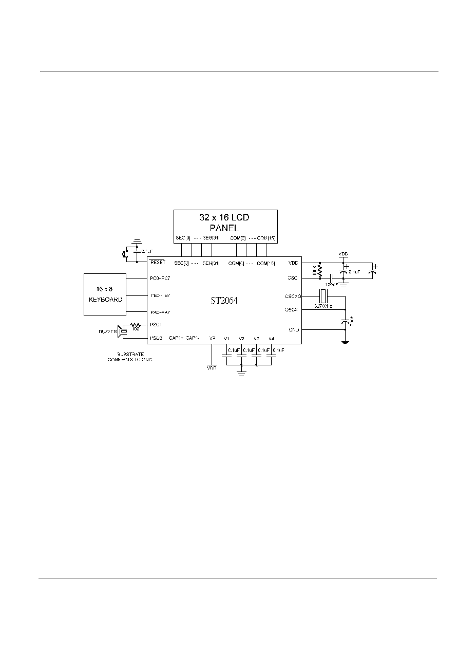
Sitronix ST2064
Ver 1.0
43/46
10/11/02
18.2 APPLICATION CIRCUIT UNDER 5V OPERATING VOLTAGE
VDD : 5V
Clock : 32768Hz crystal and 2.0MHz RC oscillator
LCD : 1/16 duty
I/O
: PORT A
ALARM
: PSG0, PSG1
FIGURE 18-3 APPLICATION CIRCUIT WITHOUT DC-DC CONVERTER

Sitronix ST2064
Ver 1.0
44/46
10/11/02
1
1
9
9
.
.
P
P
A
A
D
D
C
C
E
E
N
N
T
T
E
E
R
R
C
C
O
O
O
O
R
R
D
D
I
I
N
N
A
A
T
T
E
E
S
S
Chip size: 2660�m X 2930�m
Coordinate: Pad center (�m)
Origin: Chip center
Pad pitch: 110�m, 120�m
Substrate connection: GND
Unit: �m
PAD NO.
NAME
X
Y
PAD NO.
NAME
X
Y
1
OSCXO
-1290.00
1235.20
31
COM8
-382.90
-1383.60
2
OSCXI
-1290.00
1115.20
32
COM9
-262.90
-1383.60
3
RESET
-1290.00
995.20
33
COM10
-142.90
-1383.60
4
OSCI
-1290.00
875.20
34
COM11
-22.90
-1383.60
5
XIO
-1290.00
765.20
35
COM12
97.10
-1383.60
6
GND
-1290.00
655.20
36
COM13
217.10
-1383.60
7
VDD
-1290.00
545.20
37
COM14
337.10
-1383.60
8
PA0
-1290.00
435.20
38
COM15
457.10
-1383.60
9
PA1
-1290.00
325.20
39
SEG0
577.10
-1383.60
10
PA2
-1290.00
215.20
40
SEG1
697.10
-1383.60
11
PA3
-1290.00
105.20
41
SEG2
817.10
-1383.60
12
PA4
-1290.00
-4.80
42
SEG3
937.10
-1383.60
13
PA5
-1290.00
-114.80
43
SEG4
1057.10
-1383.60
14
PA6
-1290.00
-224.80
44
SEG5
1177.10
-1383.60
15
PA7
-1290.00
-334.80
45
SEG6
1222.30
-1244.85
16
CAP1+
-1290.00
-444.80
46
SEG7
1222.30
-1124.85
17
CAP1-
-1290.00
-554.80
47
SEG8
1222.30
-1004.85
18
V4
-1290.00
-664.80
48
SEG9
1222.30
-884.85
19
V3
-1290.00
-774.80
49
SEG10
1222.30
-774.85
20
V2
-1290.00
-884.80
50
SEG11
1222.30
-664.85
21
V1
-1290.00
-1004.80
51
SEG12
1222.30
-554.85
22
VP
-1290.00
-1124.80
52
SEG13
1222.30
-444.85
23
COM0
-1290.00
-1244.80
53
SEG14
1222.30
-334.85
24
COM1
-1222.90
-1383.60
54
SEG15
1222.30
-224.85
25
COM2
-1102.90
-1383.60
55
SEG16
1222.30
-114.85
26
COM3
-982.90
-1383.60
56
SEG17
1222.30
-4.85
27
COM4
-862.90
-1383.60
57
SEG18
1222.30
105.15
28
COM5
-742.90
-1383.60
58
SEG19
1222.30
215.15
29
COM6
-622.90
-1383.60
59
SEG20
1222.30
325.15
30
COM7
-502.90
-1383.60
60
SEG21
1222.30
435.15

Sitronix ST2064
Ver 1.0
45/46
10/11/02
PAD NO.
NAME
X
Y
PAD NO.
NAME
X
Y
61
SEG22
1222.30
545.15
76
SEG37/PC5
265.05
1402.75
62
SEG23
1222.30
655.15
77
SEG38/PC6
145.05
1402.75
63
SEG24
1222.30
765.15
78
SEG39/PC7
25.05
1402.75
64
SEG25
1222.30
875.15
79
SEG40/PB0
-94.95
1402.75
65
SEG26
1222.30
995.15
80
SEG41/PB1
-214.95
1402.75
66
SEG27
1222.30
1115.15
81
SEG42/PB2
-334.95
1402.75
67
SEG28
1222.30
1235.15
82
SEG43/PB3
-454.95
1402.75
68
SEG29
1222.30
1402.75
83
SEG44/PB4
-574.95
1402.75
69
SEG30
1102.30
1402.75
84
SEG45/PB5
-690.00
1402.75
70
SEG31
982.30
1402.75
85
SEG46/PB6
-810.00
1402.75
71
SEG32/PC0
862.30
1402.75
86
SEG47/PB7
-930.00
1402.75
72
SEG33/PC1
742.30
1402.75
87
PSG0
-1050.00
1402.75
73
SEG34/PC2
625.05
1402.75
88
PSG1
-1170.00
1402.75
74
SEG35/PC3
505.05
1402.75
89
TEST
-1290.00
1402.75
75
SEG36/PC4
385.05
1402.75

Sitronix ST2064
Ver 1.0
46/46
10/11/02
2
2
0
0
.
.
R
R
E
E
V
V
I
I
S
S
I
I
O
O
N
N
S
S
Version 1.0:
PAGE42 Modify FIGURE 18-2 scan line resister and return line cap value of keyboard.
Added the application note & pin7 connect switch to GND
PAGE40 Modify electronic characteristic table..........................................................................2002/9/11
Version 0.9:
PAGE 41/42/43:
Modify application circuit FIGURE 18-1, FIGURE 18-2, FIGURE 18-3..............................2002/7/17
Version 0.8:
PAGE 23/24/25/26/27:
Rename all PSG register "PCH" to "PSG".
PAGE 2/4/22/23/24/25/28/29/30:
Rename all PSG pad "PSG1/0" to "PSGO/PSGOB........................................................2002/6/10
Version 0.7:
PAGE 23/24/25/26/27:
Changed all "PSG1H/PSG1L" & "PSG0H/PSG0L" to "PCH1H/PCH1L" "PCH1H/PCH1L".
PAGE25 Added FIGURE 12-6 PSG application circuit and description..........................................2002/5/9
Version 0.6:
PAGE34 Modify Keyboard-scan code.....................................................................................2002/5/6
Version 0.5:
PAGE18 Modify PRES reading value
PAGE33 Modify description of "scan" bit in TABLE 14-3
PAGE1 Modify LCD driving strength of 'features' to 16 level
PAGE10 Modify item9.1Description 32 GPIOs to 24
PAGE34 Added LCD waveform & 14.3Keyboard-scan................................................................2002/4/11
Version 0.4:
PAGE41 Fill the electrical characteristics table
PAGE33 Modify driving strength control register........................................................................2002/3/11
Version 0.3:
PAGE42 Add application circuit
PAGE2 Modify pad name in pad coordinates.........................................................................2002/01/28
Version 0.2:
PAGE2 Add pad coordinates
PAGE40 Modify low voltage detector operation........................................................................2002/01/18
Version 0.1:
First release