ST
Sitronix
ST7522
17 x 96 Dot Matrix LCD Controller/Driver
Ver 1.0c
1/45
2002/07/10
O
O
V
V
E
E
R
R
V
V
I
I
E
E
W
W
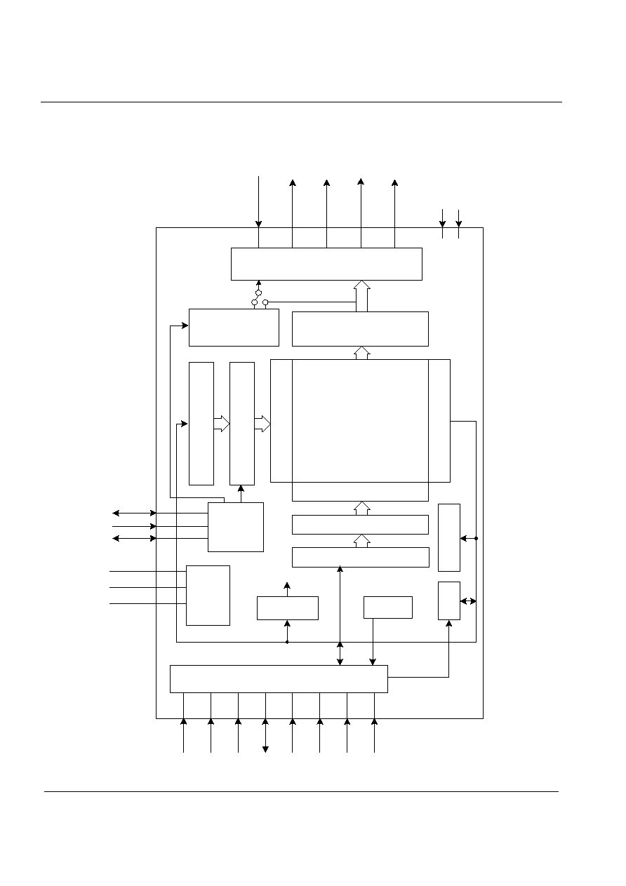
The ST7522 family of dot matrix LCD drivers are
designed for the display of characters and graphics.
The drivers generate LCD drive signals derived from bit
mapped data stored in an internal RAM.
The drivers are available in two configurations
The ST7522 family drivers incorporate innovative
circuit design strategies to achieve very low power
dissipation at a wide range of operating voltages.
These features give the designer a flexible means of
implementing small to medium size LCD displays for
compact, low power systems.
The ST7522 which is able to drive 1 line of 6 Chinese
characters or 2 lines of 12 Chinese characters each
line
with two ST7522.
F
F
E
E
A
A
T
T
U
U
R
R
E
E
S
S
Fast 8-bit MPU interface compatible with 80- and
68- family microcomputers and serial interface
Clock synchronous serial interface
Many
command
set
Display data Read/Write, display ON/OFF,
Normal/Reverse display mode, page address set ,
column address set , status read , display all
points ON/OFF, LCD bias set, electronic volume,
read/modify/write, segment driver direction select,
power saver, static indicator, adjustable OSC
frequency, booster input voltage select, follower
input voltage and amplified ratio selectable
4
static
indicator
and 96 icon available
Total 118 (segment + common + static) drive sets
Wide range of supply voltages
V
DD
� V
SS
2.7 to 5.5 V
V
DD
� V
5
3.5 to 7.0 V
V
DD
� V
CAP3
3.5 to 7.0 V
Low-power
CMOS
64 level digital contrast control
Clock frequency
Product
name
On-Chip External
Number
of COM
Number
of SEG
Bias Duty
ST7522D 1.2KHz,2.4KHz
(When VDD=3.0V)
2.8KHz
17
96
1/5,1/6 1/17,1/33
ST7522
Ver 1.0c
2/45
2002/07/10
ST7522 Serial Specification Revision History
Version
Date
Description
1.0 2002/01/30
New
specification
version
1.0a 2002/02/20
Modify
cover page's product name
1.0b
2002/03/18 Adding FR frequency for "OSC frequency set" command
1.0c 2002/07/10
1.
Adding "Slave chip notice" in application circuit
2.
Adding "Software example"
3.
Adding "Follower-contrast curve"
4.
Adding "Master mode application circuit"
5.
Adding "I/O pad configuration"
ST7522
Ver 1.0c
4/45
2002/07/10
P
P
A
A
D
D
A
A
R
R
R
R
A
A
N
N
G
G
E
E
M
M
E
E
N
N
T
T
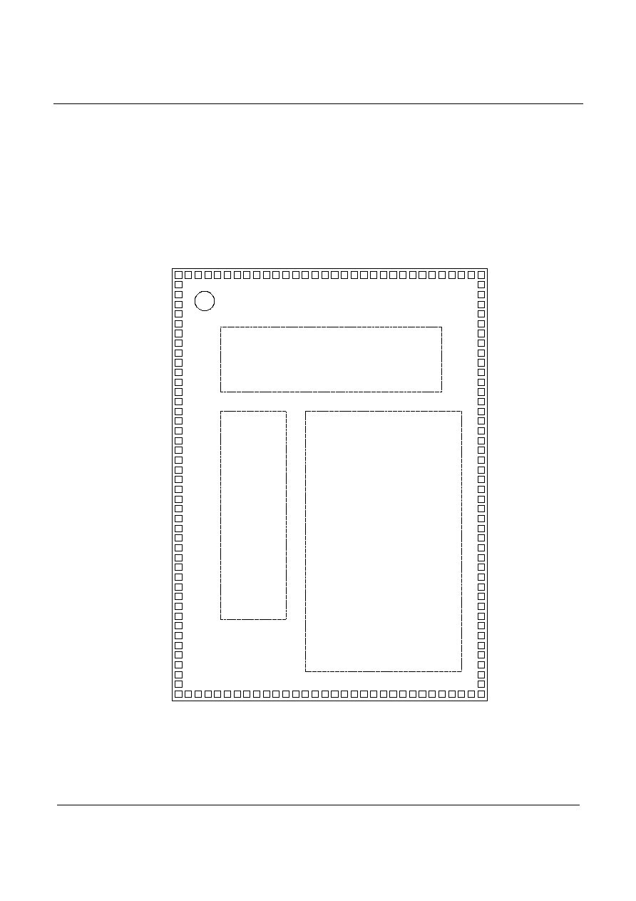
Chip specifications of AL pad package
Chip size : 3720 �m x 5040 �m
Minimum pad pitch : 110�m
Pad size : 90�m X 90�m
*
*
S
S
u
u
b
b
s
s
t
t
r
r
a
a
t
t
e
e
c
c
o
o
n
n
n
n
e
e
c
c
t
t
t
t
o
o
V
V
D
D
D
D
.
.
45
46
47
48
49
50
51
52
53
54
55
56
57
58
59
60
61
62
63
64
65
66
67
68
69
70
71
72
73
74
1
2
3
4
5
6
7
8
9
10
11
12
13
14
15
16
17
18
19
20
21
22
23
24
25
26
27
28
29
30
31
32
33
34
35
36
37
38
39
40
41
42
43
44
75
76
77
78
79
80
81
82
83
84
85
86
87
88
89
90
91
92
93
94
95
96
97
98
99
100
101
102
103
104
105
106
107
108
109
110
111
112
113
114
115
116
117
118
119
120
121
122
123
124
125
126
127
128
129
130
131
132
133
134
135
136
137
138
139
140
141
142
143
144
145
146
147
148
SEG12/
SEG11/
SEG10/
SEG9/
SEG8/
SEG7/
SEG6/
SEG5/
SEG4/
SEG3/
SEG2/
SEG1/
SEG0/
CO
MI/
C
O
M15/
C
O
M14/
C
O
M13/
C
O
M12/
C
O
M11/
C
O
M10/
CO
M9
/
CO
M8
/
CO
M7
/
CO
M6
/
CO
M5
/
CO
M4
/
CO
M3
/
CO
M2
/
CO
M1
/
CO
M0
/
SEG29
SEG28
SEG27
SEG26
SEG25
SEG24
SEG23
SEG22
SEG21
SEG20
SEG19
SEG18
SEG17
SEG16
SEG15
SEG14
SEG13
SEG12
SEG11
SEG10
SEG9
SEG8
SEG7
SEG6
SEG5
SEG4
SEG3
SEG2
SEG1
SEG0
COM0
COM1
COM2
COM3
COM4
COM5
COM6
COM7
COM8
COMS
S1
S2
S3
S4
P/S
CL
VSS
D0
D1
D2
D3
D4
D5
D6
D7
/CS1
CS2
E(RD)
A0
R/W
VDD
C86
RES
CLS
FR
V1
V4
V3
M/S
V5
V2
CAP1
CAP2
CAP3
SEG95/
SEG94/
SEG93/
SEG92/
SEG91/
SEG90/
SEG89/
SEG88/
SEG87/
SEG86/
SEG85/
SEG84/
SEG83/
SEG82/
SEG81/
SEG80/
SEG79/
SEG78/
SEG77/
SEG76/
SEG75/
SEG74/
SEG73/
SEG72/
SEG71/
SEG70/
SEG69/
SEG68/
SEG67/
SEG66/
SEG65/
SEG64/
SEG63/
SEG62/
SEG61/
SEG60/
SEG59/
SEG58/
SEG57/
CO
M9
CO
M1
0
CO
M1
1
CO
M1
2
CO
M1
3
CO
M1
4
CO
M1
5
CO
MI
SEG95
SEG94
SEG93
SEG92
SEG91
SEG90
SEG89
SEG88
SEG87
SEG86
SEG85
SEG84
SEG83
SEG82
SEG81
SEG80
SEG79
SEG78
SEG77
SEG76
SEG75
SEG74
SEG73
SEG72
SEG71
SEG70
SEG69
SEG68
SEG67
SEG66
SEG65
SEG64
SEG63
SEG62
SEG61
SEG60
SEG59
SEG58
SEG57
SEG56
SEG55
SEG54
SEG53
SEG52
SEG51
SEG50
SEG49
SEG48
SEG47
SEG46
SEG45
SEG44
SEG43
SEG42
SEG41
SEG40
SEG39
SEG38
SEG37
SEG36
SEG35
SEG34
SEG33
SEG32
SEG31
SEG30
/SEG56
/SEG55
/SEG54
/SEG53
/SEG52
/SEG51
/SEG50
/SEG49
/SEG48
/SEG47
/SEG46
/SEG45
/SEG44
/SEG43
/SEG42
/SEG41
/SEG40
/SEG39
/SEG38
/SEG37
/SEG36
/SEG35
/SEG34
/SEG33
/SEG32
/SEG31
/SEG30
/SEG29
/SEG28
/SEG27
/SEG26
/SEG25
/SEG24
/SEG23
/SEG22
/SEG21
/SEG20
/SEG19
/SEG18
/SEG17
/SEG16
/SEG15
/SEG14
/SEG13

ST7522
Ver 1.0c
5/45
2002/07/10
P
P
A
A
D
D
C
C
E
E
N
N
T
T
E
E
R
R
C
C
O
O
O
O
R
R
D
D
I
I
N
N
A
A
T
T
E
E
S
S
(chip size : 3720 �m x 5040 �m)
Pin Name
Pin Name
Pin Name
Pad
No. Master Slave
X
Y
Pad
No. Master Slave
X
Y
Pad
No.
Master Slave
X
Y
1 SEG56
SEG73
-1745 2405 50 SEG7 SEG24 -1045 -2405
99
CLS
1745
275
2 SEG55
SEG72
-1745 2275 51 SEG6 SEG23
-935
-2405
100
FR
1745
385
3 SEG54
SEG71
-1745 2155 52 SEG5 SEG22
-825
-2405
101
V1
1745
495
4 SEG53
SEG70
-1745 2035 53 SEG4 SEG21
-715
-2405
102
V4
1745
605
5 SEG52
SEG69
-1745 1925 54 SEG3 SEG20
-605
-2405
103
V3
1745
715
6 SEG51
SEG68
-1745 1815 55 SEG2 SEG19
-495
-2405
104
M/S
1745
825
7 SEG50
SEG67
-1745 1705 56 SEG1 SEG18
-385
-2405
105
V5
1745
935
8 SEG49
SEG66
-1745 1595 57 SEG0 SEG17
-275
-2405
106
V2
1745
1045
9 SEG48
SEG65
-1745 1485 58 COMI
SEG16
-165
-2405
107
CAP1
1745
1155
10 SEG47
SEG64
-1745 1375 59 COM15 SEG15
-55 -2405
108
CAP2
1745
1265
11 SEG46
SEG63
-1745 1265 60 COM14 SEG14
55 -2405
109
CAP3
1745
1375
12 SEG45
SEG62
-1745 1155 61 COM13 SEG13
165
-2405
110
SEG95
COM0
1745
1485
13 SEG44
SEG61
-1745 1045 62 COM12 SEG12
275
-2405
111
SEG94
COM1
1745
1595
14 SEG43
SEG60
-1745 935 63 COM11 SEG11
385
-2405
112
SEG93
COM2
1745
1705
15 SEG42
SEG59
-1745 825 64 COM10 SEG10
495
-2405
113
SEG92
COM3
1745
1815
16 SEG41
SEG58
-1745 715 65 COM9
SEG9
605
-2405
114
SEG91
COM4
1745
1925
17 SEG40
SEG57
-1745 605 66 COM8
SEG8
715
-2405
115
SEG90
COM5
1745
2035
18 SEG39
SEG56
-1745 495 67 COM7
SEG7
825
-2405
116
SEG89
COM6
1745
2155
19 SEG38
SEG55
-1745 385 68 COM6
SEG6
935
-2405
117
SEG88
COM7
1745
2275
20 SEG37
SEG54
-1745 275 69 COM5
SEG5
1045
-2405
118
SEG87
COM8
1745
2405
21 SEG36
SEG53
-1745 165 70 COM4
SEG4
1155
-2405
119
SEG86
COM9
1615
2405
22 SEG35
SEG52
-1745 55 71 COM3
SEG3
1265
-2405
120
SEG85
COM10
1495
2405
23 SEG34
SEG51
-1745 -55 72 COM2
SEG2
1375
-2405
121
SEG84
COM11
1375
2405
24 SEG33
SEG50
-1745 -165 73 COM1
SEG1
1495
-2405
122
SEG83
COM12
1265
2405
25 SEG32
SEG49
-1745 -275 74 COM0
SEG0
1615
-2405
123
SEG82
COM13
1155
2405
26 SEG31
SEG48
-1745 -385 75
COMS
1745
-2405
124
SEG81
COM14
1045
2405
27 SEG30
SEG47
-1745 -495 76
S1
1745
-2275
125
SEG80
COM15
935
2405
28 SEG29
SEG46
-1745 -605 77
S2
1745
-2155
126
SEG79
COMI
825
2405
29 SEG28
SEG45
-1745 -715 78
S3
1745
-2035
127
SEG78
SEG95
715
2405
30 SEG27
SEG44
-1745 -825 79
S4
1745
-1925
128
SEG77
SEG94
605
2405
31 SEG26
SEG43
-1745 -935 80
P/S
1745
-1815
129
SEG76
SEG93
495
2405
32 SEG25
SEG42
-1745 -1045 81
CL
1745
-1705
130
SEG75
SEG92
385
2405
33 SEG24
SEG41
-1745 -1155 82
VSS
1745
-1595
131
SEG74
SEG91
275
2405
34 SEG23
SEG40
-1745 -1265 83
D0
1745
-1485
132
SEG73
SEG90
165
2405
35 SEG22
SEG39
-1745 -1375 84
D1
1745
-1375
133
SEG72
SEG89
55 2405
36 SEG21
SEG38
-1745 -1485 85
D2
1745
-1265
134
SEG71
SEG88
-55 2405
37 SEG20
SEG37
-1745 -1595 86
D3
1745
-1155
135
SEG70
SEG87
-165
2405
38 SEG19
SEG36
-1745 -1705 87
D4
1745
-1045
136
SEG69
SEG86
-275
2405
39 SEG18
SEG35
-1745 -1815 88
D5
1745
-935
137
SEG68
SEG85
-385
2405
40 SEG17
SEG34
-1745 -1925 89
D6
1745
-825
138
SEG67
SEG84
-495
2405
41 SEG16
SEG33
-1745 -2035 90
D7
1745
-715
139
SEG66
SEG83
-605
2405
42 SEG15
SEG32
-1745 -2155 91
/CS1
1745
-605
140
SEG65
SEG82
-715
2405
43 SEG14
SEG31
-1745 -2275 92
CS2
1745
-495
141
SEG64
SEG81
-825
2405
44 SEG13
SEG30
-1745 -2405 93
E(RD)
1745
-385
142
SEG63
SEG80
-935
2405
45 SEG12
SEG29
-1615 -2405 94
A0
1745
-275
143
SEG62
SEG79
-1045
2405
46 SEG11
SEG28
-1495 -2405 95
R/W
1745
-165
144
SEG61
SEG78
-1155
2405
47 SEG10
SEG27
-1375 -2405 96
VDD
1745
-55 145
SEG60
SEG77
-1265
2405
48 SEG9
SEG26
-1265 -2405 97
C86
1745
55 146
SEG59
SEG76
-1375
2405
49 SEG8
SEG25
-1155 -2405 98
RES
1745
165
147
SEG58
SEG75
-1495
2405
148
SEG57
SEG74
-1615
2405