ST
Sitronix
ST8601
PRELIMINARY
162 Channel Common Driver for STN LCD with High-Voltage Drive
Notice: This is not a final specification. Some parameters are subject to change
Ver 0.02
1/19
2001/Dec/13
1
1
F
F
e
e
a
a
t
t
u
u
r
r
e
e
s
s
Duty cycle up to 1/162
LCD drive voltage: 40V max
Built-in switching circuit (generate �19.7V)
162 LCD drive circuits
Operating voltage: 2.5 to 5.5 V
Built-in alternating signal generating circuit (Pin
programmable)
Display-off function
120/160/162 output mode
2
2
D
D
e
e
s
s
c
c
r
r
i
i
p
p
t
t
i
i
o
o
n
n
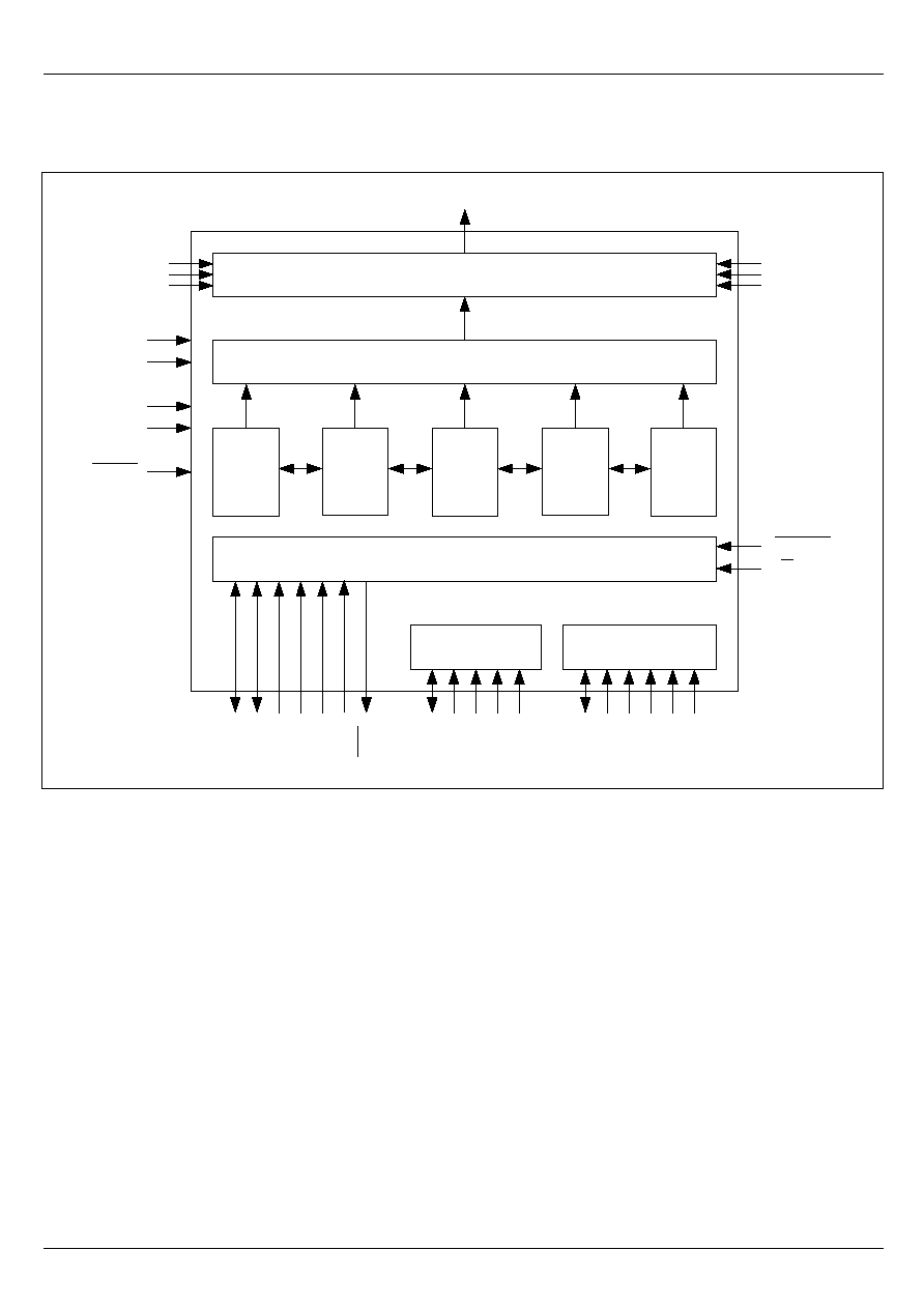
The ST8601 is a 162-channel common driver that drives a
dot matrix LCD panel. By changing the mode, this can be
applied to 162, 160 and 120 channel output. Through the
use of a 40V high voltage CMOS process technology, a
high voltage drive of +20V, centering on V
M,
is
possible. �20V generated from +20V with built-in switching
circuit and external capacitor. Low logic drive voltage is
used. This device is used together with the segment driver
ST8616, ST8624 or ST8632.

Sitronix ST8601
Ver 0.02
4/19
2001/Dec/13
5
5
B
B
l
l
o
o
c
c
k
k
F
F
u
u
n
n
c
c
t
t
i
i
o
o
n
n
s
s
LCD Drive Circuit
This circuit selects and outputs the three level signals for
the LCD drive. By a combination of the data in the shift
register and M, either V
H
, V
L
or V
M
is selected and
transmitted to the output circuit.
Shift register
This is a 162-bit bi-directional shift register circuit. The first
line marker signal output from the DIO
1
pin and DIO
2
pin is
sequentially shifted by shift clock CL. The SHL pin
determines the shift direction.
Level shifter
This boosts a logic signal to a high voltage signal for LCD
drive.
Alternation signal generating circuit
This circuit generates an alternating signal (M signal) for
LCD display. To suppress cross talk, the signal is
alternated in a unit from several lines to several tens of
lines. By connecting MWS0~MWS4 pins to V
DD
or GND,
the desired number of signals can be alternated. When
alternating are externally input, all pins (MWS0 ~ MWS4)
are connected to GND.

Sitronix ST8601
Ver 0.02
5/19
2001/Dec/13
6
6
P
P
i
i
n
n
D
D
e
e
s
s
c
c
r
r
i
i
p
p
t
t
i
i
o
o
n
n
(
(
T
T
C
C
P
P
)
)
PIN NO.
SYMBOL
I/O
DESCRIPTION
1~162 X1~X162
O
Either level V
H
, V
L
or V
M
is output according to the combination of the M signal and
display data when the DISPOFF pin is set at V
DD
. See figure 3
163,164
194,195
193,165
166,167
191,192
V
HR
VHL
V
ML
, V
MR
V
LR
V
LL
P
LCD drive-level voltage.
V
HL
, V
HR
, V
LL
, V
LR
: selected level. V
ML
, V
MR
: non-selected level
179,172 V
DD
, GND
P Logic power supply
190 VEO
P
When the built-in switching circuit is use to generate V
L
, VEO pin is connected to
V
LL, R
pins. V
M
voltage is a reference point and reversed and output the voltage
input to the voltage between V
LCD
and V
M
. If built-in switching circuit is not used,
don't connect any lines to this pin.
189,188 C1,
C2 I
External capacitor should be connected here when switching circuit is used for
generating V
L
, otherwise do not connect any lines to this pin.
171 CL
I
Shift clock input. Data is shifted at the falling edge of shift clock CL of the shift
register.
186
M
I/O Inputs or outputs the alternating signal for LCD drive output.
180~184 MWS0~MWS4 I
This pin specifies the cycle of the alternating signal (M) in the unit of the number of
lines. The number of lines, which is an integer from 2 to 31or one frame, is specified
as follows. Usually, specify the number of lines within a range from 10 to 31 or one
frame.
Table-1
177
178
MODE0
MODE1
I
Input pin for selecting the number of LCD drive outputs. Table-3.
When 160-output mode, output pins which aren't use (X1
,
X162) output the
non-select level.
When 120-output mode, output pins which aren't use (X1, X62~X101, X162) output
the non-select level.
168,187
DIO
1
, DIO
2
I/O Serial data input pin. Table-2
170 CCL
I
Built-in switching circuit clock input. When use built-in switching circuit and generate
V
L
, this pin connect CL pin. If built-in switching circuit is not used, CCL must be fixed
to GND.
174 AMP
I
Built-in switching circuit on-off control. When use built-in switching circuit, this pin
must be fixed to V
DD
. If built-in switching circuit is not used, this pin must be fixed to
GND.
185 RESET
I
Setting this pin to GND sets initializes the alternating signal (M) circuit. A V
DD
level
RESET is normally used.