 | –≠–ª–µ–∫—Ç—Ä–æ–Ω–Ω—ã–π –∫–æ–º–ø–æ–Ω–µ–Ω—Ç: AP121-89 | –°–∫–∞—á–∞—Ç—å:  PDF PDF  ZIP ZIP |
Skyworks Solutions, Inc. [978] 241-7000
∑
Fax [978] 241-7906
∑
Email sales@skyworksinc.com
∑
www.skyworksinc.com
1
Specifications subject to change without notice. 3/99A
GaAs IC 3 Stage GSM Power Amplifier
Features
+3.5 V Operation
Output Power of 35 dBm
Efficiency Typically 55%
Outstanding Efficiency vs. Supply Voltage
High Power SSOP-16 Package with
Exposed Pad
Wide Power Control Range (70 dB)
Designed to work with AP122-89 as a
Dualband Solution
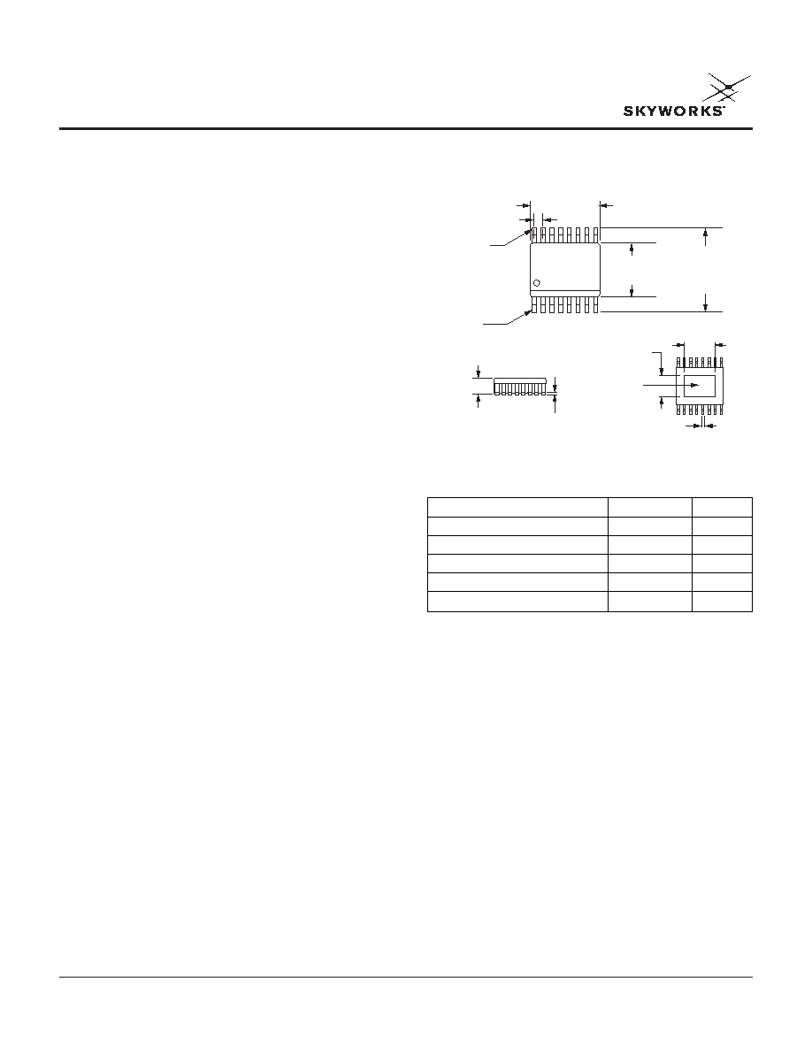
SSOP-16 with Exposed Pad
AP121-89
Description
The AP121-89 is a low cost IC power amplifier designed for
the 880≠915 MHz frequency band. It features single supply,
3.5 V battery operation and exceptional efficiency. Drive level
requirements are minimized with 3 stages of amplification,
thereby reducing the cost of the VCO. The AP121-89 is
designed to be stable over a temperature range of -40 to
+85∞C and over a 10:1 output VSWR load. External
matching is used for improved performance and flexibility.
0.197 (5.00 mm)
0.189 (4.80 mm)
0.158 (4.00 mm)
0.150 (3.80 mm)
0.244
(6.20 mm)
0.228
(5.80 mm)
0.025
(0.635 mm) TYP.
PIN 1
PIN 16
0.063
(1.60 mm) MAX.
0.004 (0.10 mm)
0.000 (0.00 mm)
0.095 (2.42 mm)
0.085 (2.16 mm)
EXPOSED
PAD
0.12 (0.30 mm)
0.008 (0.20 mm)
0.135 (3.43 mm)
0.125 (3.17 mm)
Preliminary
Quantity
Value
Unit
Amplifier Supply Voltage (V
DS
)
10
V
Input RF Power (P
IN
)
14
dBm
Duty Cycle
50
%
Operating Temperature (T
OP
)
-40 to +85
∞C
Storage Temperature (T
ST
)
-65 to +150
∞C
Absolute Maximum Ratings
Output Matching Circuit
The output match for the AP121-89 is provided externally
in order to improve performance, reduce cost, and add
flexibility. By making use of ceramic surface mount
components with better Qs than GaAs matching
elements, a lower loss matching network can be made.
This lower loss results in higher power and efficiency for
the amplifier. Also, by keeping these elements external the
GaAs die size is reduced and the overall cost is less. This
approach also permits the flexibility to tweak the amplifier
for optimum performance at different powers, and/or
frequencies.

GaAs IC 3 Stage GSM Power Amplifier
AP121-89
2
Skyworks Solutions, Inc. [978] 241-7000
∑
Fax [978] 241-7906
∑
Email sales@skyworksinc.com
∑
www.skyworksinc.com
Specifications subject to change without notice. 3/99A
Parameter
Symbol
Condition
Min.
Typ.
Max.
Unit
Output Power
P
OUT
T
OP
= +25∞C
34.5
35
dBm
V
DS
= 2.8 V,
32.5
33
T
OP
= (-40 to +85∞C)
Power Added Efficiency
n
PAE
50
55
%
Control Voltage Range
V
GG
-3
-1
V
2nd Harmonic
H
2
-43
-40
dBc
3rd Harmonic
H
3
-48
-45
dBc
Input VSWR
VSWR
IN
P
OUT
(5≠35 dBm), Controlled by V
GG
3:1
2:1
Forward Isolation
P
OUT, STANDBY
P
IN
= 10 dBm, V
GG
= -3.0 V
-49
-40
dBm
Switching Time
t
R
, t
F
Time from P
OUT
= -10 dBm
1
2
µ
S
to P
OUT
= 34.5 dBm
Burn Out
BO
V
DS
= 2.8 V to 6.0 V,
No Module Damage
P
IN
= 0 dBm to 10 dBm,
or Permanent Degradation
Z
S
= 50
, Load
VSWR = 10:1, All Phase Angles
Stability
Stab.
All Combinations of the Following
No Parasitic Oscillations
Parameters: I
DS
= 0A to xA,
Above -36 dBm
x = Current at P
OUT
= 34.5 dBm in 50
P
IN
= 3 dBm to 10 dBm,
V
DS
= 2.5 V to 4.5 V,
T
OP
= -40 to +85∞C,
Load VSWR = 10:1, All Phase Angles
Slope P
OUT
/V
GG
P
OUT
= -15 dBm to 35 dBm
10
100
150
dB/V
Noise Power
100 KHz BW
-90
-85
dBm
925-960 MHz Band
Phase Change
AM-PM
The Change in Phase When
5
10
Deg.
P
OUT
Changes from 33 dBm to 34 dBm
Electrical Specifications at 25∞C
Characteristic Values:
P
IN
= 3 dBm
fc = 880≠915 MHz
V
DS
= 3.5 V
T
OP
= +25∞C
V
GG
= Switched at 217 Hz with Duty Cycle of 12.5%

GaAs IC 3 Stage GSM Power Amplifier
AP121-89
Skyworks Solutions, Inc. [978] 241-7000
∑
Fax [978] 241-7906
∑
Email sales@skyworksinc.com
∑
www.skyworksinc.com
3
Specifications subject to change without notice. 3/99A
PAE (%)
GSM PA - Gate Sweep
P
IN
= 3 dBm, V
DD
= 3.5 V,
Frequency = 902 MHz
-30
-25
-20
-15
-10
-5
0
5
10
15
20
25
30
35
40
0
10
20
30
40
50
60
70
V
GG
- Gate Voltage (V)
Output Power (dBm)
-3.0
-2.8
-2.6
-2.4
-2.2
-2.0
-1.8
-1.6
P
OUT
PAE
Input Power (dBm)
P
OUT
(dBm) & Gain (dB)
PAE (%)
GSM PA - Power Sweep
V
G
= -1.9 V, V
DD
= 3.5 V,
Frequency = 902 MHz
-10
-5
0
5
10
15
20
25
30
35
40
45
50
-15 -13 -11 -9 -7 -5 -3 -1
1
3
5
7
0
10
20
30
40
50
60
P
OUT
Gain
PAE
PAE (%)
GSM PA - Gate Sweep
P
IN
= 3 dBm, V
DD
= 2.8 V,
Frequency = 902 MHz
-30
-25
-20
-15
-10
-5
0
5
10
15
20
25
30
35
40
0
10
20
30
40
50
60
70
V
GG
- Gate Voltage (V)
Output Power (dBm)
-3.0
-2.8
-2.6
-2.4
-2.2
-2.0
-1.8
-1.6
P
OUT
PAE
Input Power (dBm)
P
OUT
(dBm) & Gain (dB)
PAE (%)
GSM PA - Power Sweep
V
G
= -1.9 V, V
DD
= 2.8 V,
Frequency = 902 MHz
-10
-5
0
5
10
15
20
25
30
35
40
45
50
-15 -13 -11 -9 -7 -5 -3 -1
1
3
5
7
0
10
20
30
40
50
60
P
OUT
Gain
PAE
Typical Performance Data

GaAs IC 3 Stage GSM Power Amplifier
AP121-89
4
Skyworks Solutions, Inc. [978] 241-7000
∑
Fax [978] 241-7906
∑
Email sales@skyworksinc.com
∑
www.skyworksinc.com
Specifications subject to change without notice. 3/99A
1
GND
V
DS2
N/C
V
DS1
GND
GND
RF In
V
GS1
RF Out/V
DS3
RF Out
RF Out
RF Out
GND
GND
V
GS3
V
GS2
23
45
6
8
16
15
14
13
12
11
9
7
10
Pin Out
Pin Configuration
Terminal
Symbol
Function
1 GND
Ground
2 V
DS2
Stage 2 Drain Voltage
3 N/C
No
Connect
4 V
DS1
Stage 1 Drain Voltage
5 GND
Ground
6 GND
Ground
7
RF IN
RF Input
8 V
GS1
Stage 1 Gate Voltage
9 V
GS2
Stage 2 Gate Voltage
10
V
GS3
Stage 3 Gate Voltage
11
GND Ground
12
GND Ground
13
RF Out
RF Output
14
RF Out
RF Output
15
RF Out
RF Output
16
RF Out/V
DS3
RF Output/Stage 3 Drain Voltage