Skyworks Solutions, Inc. [781] 376-3000
∑ Fax [781] 376-3100 ∑ Email sales@skyworksinc.com ∑ www.skyworksinc.com
1
Specifications subject to change without notice. 2/03A
Parameter
Condition
Symbol
Min.
Typ.
Max.
Unit
Frequency Range
MHz
1800
2500
dB
Small Signal Gain
F = 2.45 GHz
S
21
17
19
22
dB
Output Power at 1 dB compression
F = 2.45 GHz
P
1 dB
26
27
dBm
Linear Output Power
1
F = 2.45 GHz, I
C
= 186 mA
P
Out
23
23.5
dBm
First Sidelobe
1
F = 2.45 GHz, I
C
= 170 mA,
-40
dBc
P
Out
= 22.5 dBm
Second Sidelobe
1
F = 2.45 GHz, I
C
= 186 mA,
-54
dBc
P
Out
= 22.5 dBm
Operating Voltage
Amplifier DC voltage
V
D
2.5
3.3
4.5
V
Reverse Isolation
Isol.
30
dB
Current Consumption
P
Out
= 23.5 dBm
186
mA
P
Out
= 22.5 dBm
170
mA
P
Out
= 17 dBm
120
mA
Quiescent
I
QO
90
mA
3.3 V, 802.11b/g
Linear Power Amplifier
Features
High Linearity @ 23 dBm
DC Current: 180 mA @ 3.3 V
802.11b/g Compliant
1800≠2500 MHz Operation
19 dB Small Signal Gain
27 dBm P
1 dB
@ 2.4 GHz
Uses Single DC Bias Supply
Low Cost Plastic Package
Available on Tape & Reel
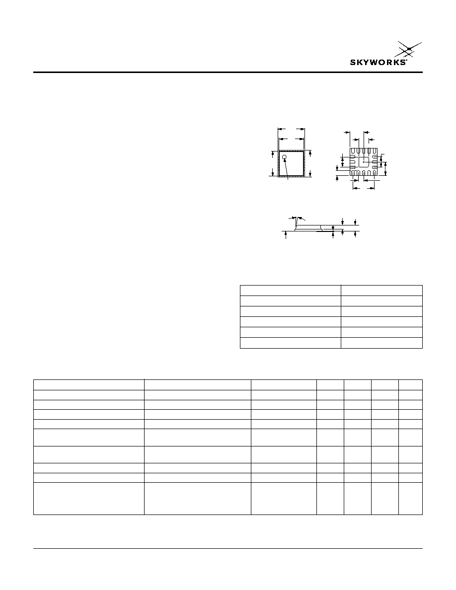
AP163-317
Description
The AP163-317 is a linear, medium power amplifier
designed for low voltage operation in 2.4≠2.5 GHz ISM
band having linear and high-efficiency performance with
802.11b/g signals. The device is manufactured on
advanced InGap HBT process and housed in a 16 Pin
4 x 4 mm micro lead package.
Electrical Specifications at 25∞C
Preliminary
Characteristic
Value
RF Input Power
20 dBm
Supply Current
800 mA
Supply Voltage
5 V
Operating Temperature
-65∞C to +125∞C
Storage Temperature
-65∞C to +125∞C
Absolute Maximum Ratings
-317
SEATING PLANE
12∞ MAX.
0.058
(1.47mm)
PIN
INDICATOR
0.058
(1.47 mm)
0.079
(2.00 mm)
0.025 (0.65 mm)
+ 0.004 (0.10 mm)
0.001 (0.025 mm)
+ 0.001 (0.025 mm)
0.039
(1.00 mm) MAX.
2
0.148
(3.75 mm)
BSC
0.157
(4.00 mm)
BSC
0.157
(4.00 mm) BSC
0.148
(3.75 mm)
BSC
1
16 1
2
0.062
(0.16 mm)
0.079
(2.00 mm)
0.031
(0.80 mm)
BSC
0.024
(0.60 mm)
REF.
0.124
(0.32 mm)
V
CC
= 3.3 V, I
C
= 90 mA (unless otherwise specified)
1. Specifications are defined for the evaluations board below with the 802.11b
signal at 11Mbit/s and having Cosine (0.95) filtering.
Pin Out
GND
N/C
V
REG
RF In
V
B
Q1
2
4
3
12
10
11
RF Out
RF Out
RF Out
V
CC1
V
CC1
V
CC1
V
B
Q2
N/C
GND
N/C
N/C
1
16
15
14
13
5
6
7
8
9
3.3 V, 802.11b/g Linear Power Amplifier
AP163-317
2
Skyworks Solutions, Inc. [781] 376-3000
∑ Fax [781] 376-3100 ∑ Email sales@skyworksinc.com ∑ www.skyworksinc.com
Specifications subject to change without notice. 2/03A
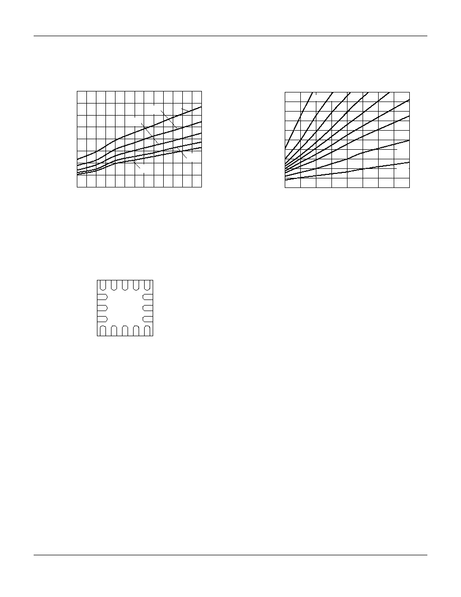
Quiescent Current of the 1st
Stage vs. V
Reg
and RQ1
0
20
40
60
80
100
120
140
160
2.0
2.2
2.4
2.6
2.8
3.0
3.2
75
100
130
150
240
V
Reg
(V)
IQ1 (mA)
Quiescent Current of the 2nd
Stage vs. V
Reg
and RQ2
V
Reg
(V)
IQ1 (mA)
0
20
40
60
80
100
120
140
160
180
200
2.5
2.6
2.7
2.8
2.9
3.0 3.1
3.2
3.3
30
39
50
75
100
10
20
240
INF
Typical Performance Data

3.3 V, 802.11b/g Linear Power Amplifier
AP163-317
Skyworks Solutions, Inc. [781] 376-3000
∑ Fax [781] 376-3100 ∑ Email sales@skyworksinc.com ∑ www.skyworksinc.com
3
Specifications subject to change without notice. 2/03A
C
10
1.5 pF
L
5
1.2 pF
C
9
C
11
20 pF
GND
GND
1
Input
2
V
B
Q1
3
V
REG
4
V
B
Q2
5
N/A
6
N/A
7
N/A
8
GND
9
Output
10
Output
11
Output
12
NC
13
V
CC1
14
V
CC1
15
V
CC1
16
AP163-317
L
4
22 nH
(0603)
10 p
0.1
µF
4.7
µF
0.1
µF
GND
V
CC
Output
C
5
2 p
C
7
560 p
GND
GND
C
6
20 p
Input
PA_PE
R
4
270
R
5
N/A
L
3
22 nH
T
1
0.35 x 0.6 mm
GND
GND
R
1
560
R
2
4.3
R
3
12 k
GND
L
1
R
6
3 k
C
12
10 pF
D
2
SMS7630
D
1
GND
C
13
100 p
R
7
56 k
+VDet
Q
1
PUMZ1
Q
2
C
1
47
µF
C
3
1 n
GND
BLM11HA471
3.3 V
3.2 V
GND
C
2
GND
C
8
C
4
GND
GND
0.35 x 6 mm
T
2
Evaluation Board Schematic
Evaluation Board Layout (Top View)
Evaluation Board Layout (Bottom View)