Skyworks Solutions, Inc. [978] 241-7000
∑ Fax [978] 241-7906 ∑ Email sales@skyworksinc.com ∑ www.skyworksinc.com
1
Specifications subject to change without notice. 10/02A
PHEMT GaAs IC High Power
SP4T Switch 0.1≠2.5 GHz
Features
4 Symmetric RF Paths
Positive Voltage Control
High IP3
Excellent Harmonic Performance
Handles GSM Power Levels
Available in 100% RF Tested Chip Form
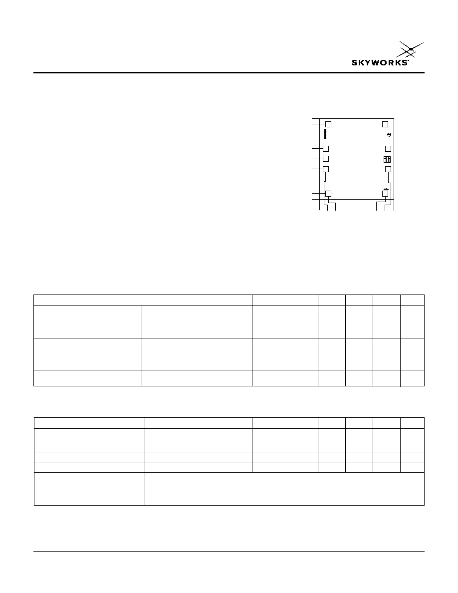
Outline Drawing
AS192-000
V
4
J
4
J
3
V
3
V
2
J
2
J
1
V
1
ANT
0.0417 (1.06 mm)
0.0387 (0.98 mm)
0.0261 (0.66 mm)
0.0209 (0.53 mm)
0.0156 (0.40 mm)
0.0030 (0.08 mm)
0.0000 (0.00 mm)
0.0000 (0.00 mm)
0.0031 (0.08 mm)
0.0045 (0.11 mm)
0.0337 (0.86 mm)
0.0351 (0.89 mm)
0.0382 (0.97 mm)
Description
The AS192-000 is a reflective SP4T switch. It is an ideal
switch for higher power applications. It can be used for
GSM dual-band handset applications where both low loss,
low current and small size are critical parameters.
Parameter
Frequency
Min.
Typ.
Max.
Unit
Insertion Loss
Ant-J
1
, J
2
, J
3
, J
4
0.1≠0.5 GHz
0.90
1.1
dB
0.5≠1.0 GHz
0.95
1.1
dB
1.0≠2.0 GHz
1.00
1.2
dB
2.0≠2.5 GHz
1.10
1.3
dB
Isolation
Ant-J
1
, J
2
, J
3
, J
4
0.1≠0.5 GHz
30
34
dB
0.5≠1.0 GHz
25
29
dB
1.0≠2.0 GHz
19
23
dB
2.0≠2.5 GHz
18
21
dB
VSWR
0.1≠1.0 GHz
1.3:1
1.0≠2.5 GHz
1.4:1
Electrical Specifications at 25∞C (0, +4.5 V)
Parameter
Condition
Frequency
Min.
Typ.
Max.
Unit
Switching Characteristics
Rise, Fall (10/90% or 90/10% RF)
50
ns
On, Off (50% CTL to 90/10% RF)
100
ns
Video Feedthru
50
mV
IP3
13 dBm/Tone
+55
dBm
2nd and 3rd Harmonics
34 dBm Input 900 MHz
+65
dBc
Control Voltages
V
Low
= 0
V
High
= +4.5 V @ 200
µA Max. for RF power > 30 dBm
V
High
= +3.0 V @ 200
µA Max. for RF power 20≠30 dBm
V
High
= +2.7 V @ 200
µA Max. for RF power < 20 dBm
Operating Characteristics at 25∞C (0, +4.5 V)
Chip thickness 0.008 ± 0.001 (0.203 ± 0.025).
PHEMT GaAs IC High Power SP4T Switch 0.1≠2.5 GHz
AS192-000
2
Skyworks Solutions, Inc. [978] 241-7000
∑ Fax [978] 241-7906 ∑ Email sales@skyworksinc.com ∑ www.skyworksinc.com
Specifications subject to change without notice. 10/02A
ANT
V
1
J
1
J
2
V
2
V
3
J
3
J
4
V
4
Pin Out
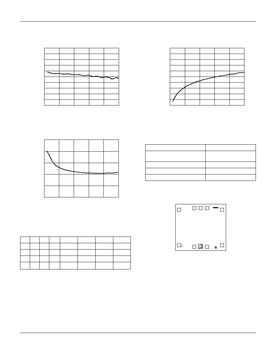
Typical Performance Data
Notes:
DC blocking caps required on RF lines for positive voltage operation
bond pad metalization: gold
backside metalization: none
bond pad dimensions: 0.003 (0.075 mm) x 0.003 (0.075 mm)
See application note, Handling GaAs MMIC Die.
Characteristic
Value
RF Input Power
4 W > 0.5 GHz
0/+6 V Control
Control Voltage
+6 V
Operating Temperature
-40∞C to +85∞C
Storage Temperature
-65∞C to +150∞C
Absolute Maximum Ratings
0
0.5
1.0
1.5
2.0
2.5
Loss (dB)
Frequency (GHz)
Typical Insertion Loss vs. Frequency
-2.0
-1.8
-1.6
-1.4
-1.2
-1.0
-0.8
-0.6
-0.4
-0.2
0
0
0.5
1.0
1.5
2.0
2.5
VSWR
Frequency (GHz)
Typical VSWR
0
0.5
1.0
1.5
2.0
2.5
0
0.5
1.0
1.5
2.0
2.5
Isolation (dB)
Frequency (GHz)
Typical Isolation vs. Frequency
-50
-45
-40
-35
-30
-25
-20
-15
-10
-5
0
V
1
V
2
V
3
V
4
Ant-J
1
Ant-J
2
Ant-J
3
Ant-J
4
V
High
V
Low
V
Low
V
Low
Ins. Loss
Isolation
Isolation
Isolation
V
Low
V
High
V
Low
V
Low
Isolation
Ins. Loss
Isolation
Isolation
V
Low
V
Low
V
High
V
Low
Isolation
Isolation
Ins. Loss
Isolation
V
Low
V
Low
V
Low
V
High
Isolation
Isolation
Isolation
Ins. Loss
Truth Table
V
Low
= 0.
V
High
= 4.5 to 5.0 V for RF power > 30 dBm.
V
High
= 3.0 to 5.0 V for RF power 20≠30 dBm.
V
High
= 2.7 to 5.0 V for RF power < 20 dBm.