 | –≠–ª–µ–∫—Ç—Ä–æ–Ω–Ω—ã–π –∫–æ–º–ø–æ–Ω–µ–Ω—Ç: AS212-93 | –°–∫–∞—á–∞—Ç—å:  PDF PDF  ZIP ZIP |
Skyworks Solutions, Inc. [781] 376-3000
∑ Fax [781] 376-3100 ∑ Email sales@skyworksinc.com ∑ www.skyworksinc.com
1
Specifications subject to change without notice. 12/02A
GaAs IC 4 x 2 Switch Matrix 0.7≠3.0 GHz
Features
Four Inputs, Two Output Switches
Any Input Can Be Directed To Either
Output
Only Requires 4 Control Lines
Low DC Power Consumption
Small Low Cost TSSOP-16 Plastic
Package
High Isolation Between Ports
Applications:
DBS Switching Applications, Cable
Modems, Cable TV
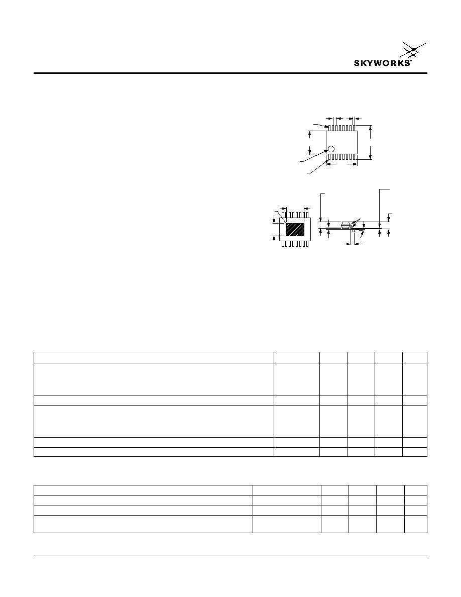
TSSOP-16
AS212-93
R 0.004
(0.09 mm) MIN.
0.010
(0.25 mm)
0∞≠8∞
A
A
0.024 (0.60 mm)
± 0.006 (0.15 mm)
0.252 (6.4 mm)
BSC
0.173 (4.40 mm)
± 0.004 (0.10 mm)
0.197 (5.00 mm)
± 0.004 (0.10 mm)
0.035 (0.90 mm)
+ 0.006 (0.15 mm)/
-0.004(-0.10 mm)
0.047
(1.20 mm)
MAX.
0.006
(0.15 mm)
MAX.
0.002
(0.05 mm)
MIN.
0.009 (0.22 mm) REF.
PIN 16
PIN 1
INDICATOR
PIN 1
0.0256 (0.65 mm) BSC
EXPOSED
PAD
0.118
(3.0 mm)
MAX.
0.118
(3.0 mm)
MAX.
Description
The AS212-93 is an IC FET 4 x 2 matrix switch in a low
cost TSSOP-16 exposed paddle plastic package. The
exposed paddle should be grounded. The AS212-93
enables 16 states directing any of the four inputs to any
of the two outputs. DC block capacitors are required at
Parameter
1
Frequency
Min.
Typ.
Max.
Unit
Insertion Loss
0.70≠0.95
6.50
7.00
dB
0.95≠1.45
6.50
7.00
dB
1.45≠2.15
6.75
7.30
dB
2.15≠3.00
7.00
7.50
dB
Insertion Loss Flatness
0.70≠3.00
1.0
2.0
dB
Isolation
0.70≠0.95
25.0
33.0
dB
0.95≠1.45
23.0
28.5
dB
1.45≠2.15
22.5
28.5
dB
2.15≠3.00
19.5
25.5
dB
Return Loss Insertion Loss State
0.70≠3.00
9
11
dB
Return Loss Isolation State
0.70≠3.00
9
11
dB
Electrical Specifications at 25∞C (0, +5 V)
1. All measurements made in a 50
system.
Parameter
Condition
Min.
Typ.
Max.
Unit
P
-1 dB
0, +5 V
12
dBm
V
CC
@ 400
µA Max.
4.5
5.5
V
Control Voltages V
1
, V
2
, V
3
, V
4
Low @ 50
µA Max.
0
0.2
V
High @ 50
µA Max.
2.5
V
CC
V
Operating Characteristics at 25∞C (0, +5 V)
each RF port. States are selected by 4 positive controls.
All ports are absorptive. The AS212-93 switch is suitable
for DBS switching applications.
2
Skyworks Solutions, Inc. [781] 376-3000
∑ Fax [781] 376-3100 ∑ Email sales@skyworksinc.com ∑ www.skyworksinc.com
Specifications subject to change without notice. 12/02A
GaAs IC 4 x 2 Switch Matrix 0.7≠3.0 GHz
AS212-93
Characteristic
Value
RF Input Power
15 dBm
Supply Voltage
+6 V
Control voltage
+6 V
Operating Temperature
-40 to +85∞C
Storage Temperature
-65 to +150∞C
Absolute Maximum Ratings
Note: Exceeding these parameters may cause irreversible damage.
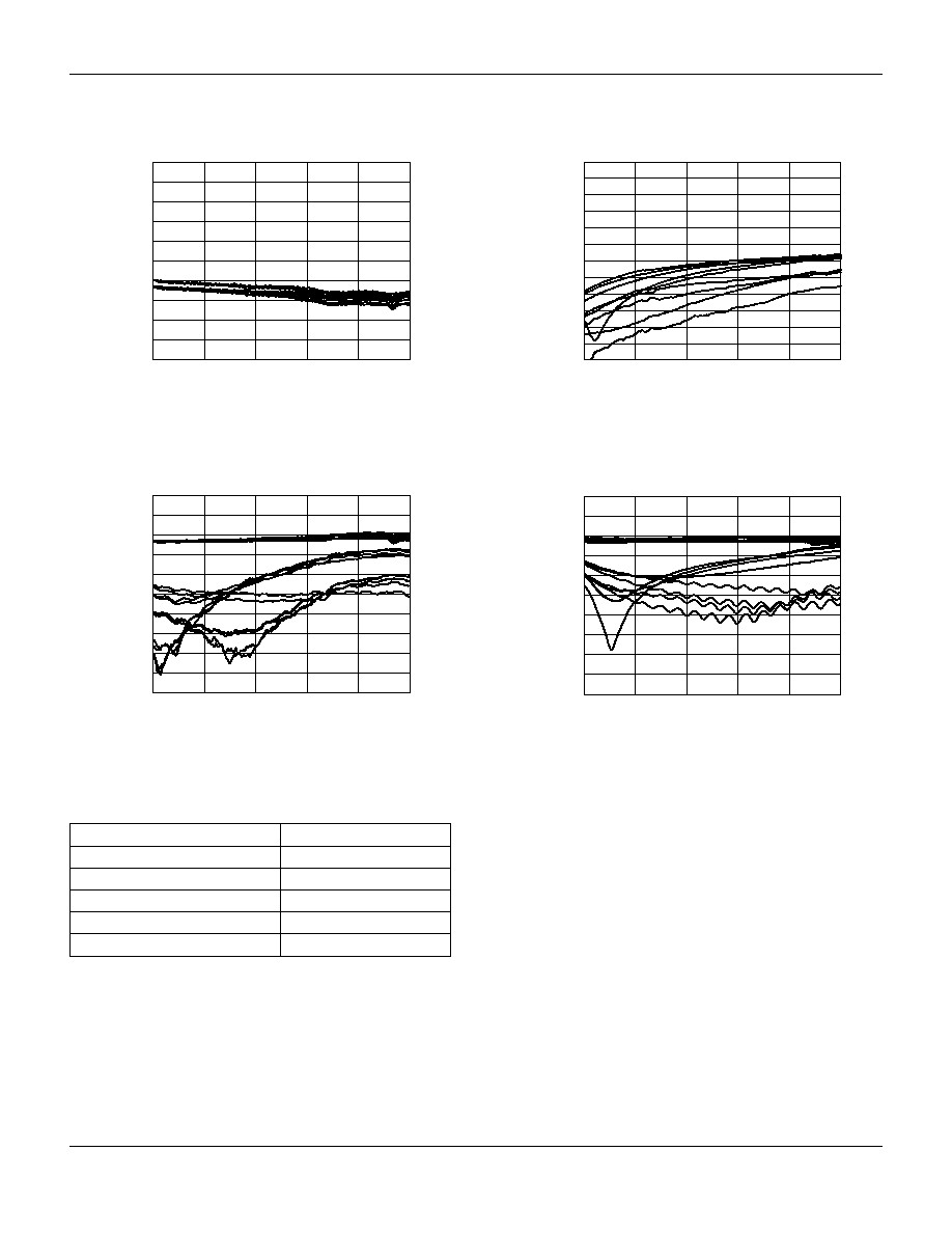
Loss (dB)
Frequency (GHz)
Typical Insertion Loss
(Various States Shown)
-10
-9
-8
-7
-6
-5
-4
-3
-2
-1
0
0.5
1.0
1.5
2.0
2.5
3.0
Return Loss S
11
and S
22
(dB)
Frequency (GHz)
Return Loss Insertion Loss State
0.5
1.0
1.5
2.0
2.5
3.0
-50
-45
-40
-35
-30
-25
-20
-15
-10
-5
0
Return Loss S
11
and S
22
(dB)
Frequency (GHz)
Return Loss Isolation State
0.5
1.0
1.5
2.0
2.5
3.0
-50
-45
-40
-35
-30
-25
-20
-15
-10
-5
0
Isolaiton (dB)
Frequency (GHz)
Typical Isolation
(Including Worst Case)
0.5
1.0
1.5
2.0
2.5
3.0
-60
-55
-50
-45
-40
-35
-30
-25
-20
-15
-10
-5
0
Typical Performance Data (0, +3 V)

Skyworks Solutions, Inc. [781] 376-3000
∑ Fax [781] 376-3100 ∑ Email sales@skyworksinc.com ∑ www.skyworksinc.com
3
Specifications subject to change without notice. 12/02A
GaAs IC 4 x 2 Switch Matrix 0.7≠3.0 GHz
AS212-93
LO
I4
RO
B1
B2
V
CC
GND
GND
A2
A1
GND
GND
GND
I3
I1
I2
1
2
34
56
8
16
15
14
13
12
11
9
7
10
Pin Out
Controls
For LO
For RO
(Left Output)
(Right Output)
Signal Path
(Insertion SW
SW
SW
SW
State #
Loss Path)
1
A1
A2
B1
B2
0
I1->LO & I1->RO
0
0
0
0
1
I1->LO & I2->RO
0
0
0
1
2
I1->LO & I3->RO
0
0
1
0
3
I1->LO & I4->RO
0
0
1
1
4
I2->LO & I1->RO
0
1
0
0
5
I2->LO & I2->RO
0
1
0
1
6
I2->LO & I3->RO
0
1
1
0
7
I2->LO & I4->RO
0
1
1
1
8
I3->LO & I1->RO
1
0
0
0
9
I3->LO & I2->RO
1
0
0
1
10
I3->LO & I3->RO
1
0
1
0
11
I3->LO & I4->RO
1
0
1
1
12
I4->LO & I1->RO
1
1
0
0
13
I4->LO & I2->RO
1
1
0
1
14
I4->LO & I3->RO
1
1
1
0
15
I4->LO & I4->RO
1
1
1
1
Truth Table
Unused leads and package bottom should be well grounded.
All paths are bidirectional.
1. All other paths are in isolation.
"1" = 5 V.
"0" = 0 V.
Bias V
CC
before applying bias to control lines.
Control lines need to be grounded for "0 V".
Control lines can not be left open circuit.
Control A1
GND
Back of Board
Control B1
SK39616
In2
In4
LO
REV 2
In3
1
Control A2
A1
A2
B1
In1
V
CC
RO
Control B2
B2
V
CC
Test Board
4
Skyworks Solutions, Inc. [781] 376-3000
∑ Fax [781] 376-3100 ∑ Email sales@skyworksinc.com ∑ www.skyworksinc.com
Specifications subject to change without notice. 12/02A
GaAs IC 4 x 2 Switch Matrix 0.7≠3.0 GHz
AS212-93
ALPHA INDUSTRIES 17540
SM
P1
30
7-
99
4
RE
V.
A
W
AF
ER
-M
UL
TI
DA
TE
C
O
DE
-9
90
3
Q
TY
. 3
00
0
CU
ST
. P
/N
- 1
33
8-
14
0-
00
0
VIS
UA
L_
_
_
_
_
_
RE
V.
C
PE
EL
T
ES
T
_
_
_
_
_
CA
UTION
ST
AT
IC
S
EN
SIT
IV
E
DE
VI
CE
S
M
AD
E I
N
U.
S.
A.
4
31
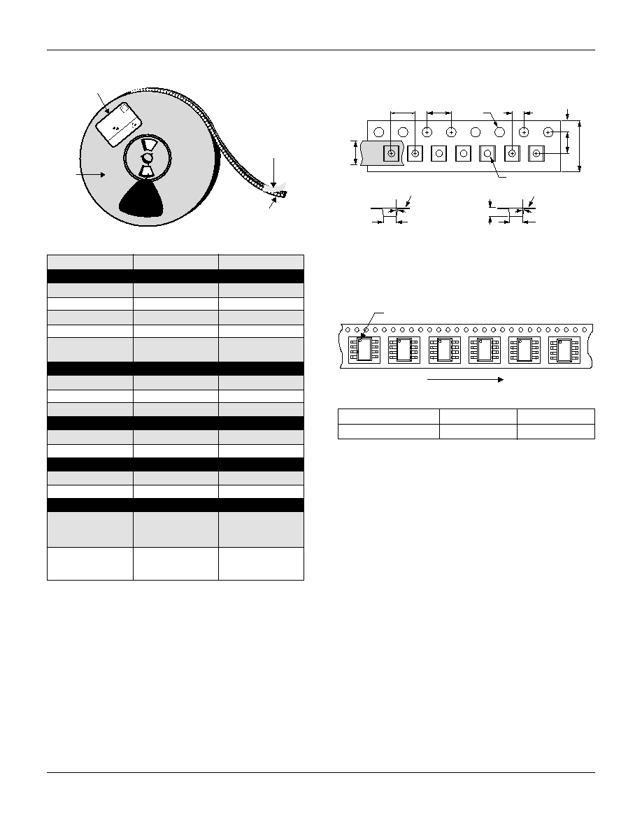
Cover Tape
Carrier Tape
Label
Reel
P
2
E
1
D
0
P
0
P
1
W
1
8∞ MAX.
A
0
B
0
D
1
W
F
T
1
(Cover Tape Thickness)
K
0
5∞ MAX.
T (Carrier Tape Thickness)
Tape Dimensions
Description
Symbol
TSSOP-16
Cavity
Length
A
0
0.80±0.10
Width
B
0
5.40±0.10
Depth
K
0
1.60±0.10
Pitch
P
1
8.00±0.10
Bottom Hole
D
1
1.60±0.10
Diameter
Perforation
Diameter
D
0
1.50±0.10
Pitch
P
0
4.00±0.10
Position
E
1
1.75±0.10
Carrier Tape
Width
W
12.0±0.30
Thickness
T
0.30±0.05
Cover Tape
Width
W
1
9.20±0.10
Tape Thickness
T
1
0.062±0.01
Distance
Cavity to
F
7.50±0.10
Perforation
(Width Direction)
Cavity to
P
2
2.00±0.1
Perforation
(Length Direction)
Note: All dimensions are in mm.
SOIC, MSOP, QSOP, SSOP and
TSSOP Devices
8, 10, 14, 16, 20, 28 Leads
User Direction of Feed
Pin 1
Standard Reel Size
7"
13"
Standard Reel Quantity
1,000
3,000