 | –≠–ª–µ–∫—Ç—Ä–æ–Ω–Ω—ã–π –∫–æ–º–ø–æ–Ω–µ–Ω—Ç: AV131-315 | –°–∫–∞—á–∞—Ç—å:  PDF PDF  ZIP ZIP |
Skyworks Solutions, Inc. [781] 376-3000
∑ Fax [781] 376-3100 ∑ Email sales@skyworksinc.com ∑ www.skyworksinc.com
1
Specifications subject to change without notice. 3/03A
HIP3TM Variable Attenuator
for AMPS and GSM Base Stations
Features
23 dB Attenuation Range
1.5 dB Insertion Loss, 1.5 SWR
0≠12 V Control Voltage
43 dBm IP3
Small Footprint LGA Package
Designed for AMPS and GSM
Base Stations
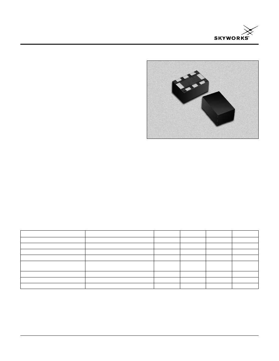
AV131-315
Description
The AV131-315 is a voltage controlled variable attenuator
from Skyworks' series of HIP3TM components. It is
specifically designed and specified for use as a wide
dynamic range low distortion attenuator for AMPS and
GSM base station applications centered at 881.5 MHz and
942.5 MHz. The AV131-315 employs a monolithic
quadrature hybrid and a pair of silicon PIN diodes to
achieve the specified low distortion performance. It
operates from 0≠12 V at 1.6 mA typical control current at
maximum attenuation. The AV131-315 is packaged in a
small outline LGA (Land Grid Array) surface mount
package with the internal elements affixed to an organic
BT substrate.
Preliminary
Parameter
Condition
Min.
Typ.
Max.
Unit
AMPS Frequency Range (BW)
869
894
MHz
GSM Frequency Range (BW)
925
960
MHz
Control Voltage (C
V
) Range
0
12
V
Insertion Loss in BW
C
V
= 0 V
1.5
dB
Attenuation Range
At F
O
, C
V
= 10 V
18
22
dB
At F
O
, C
V
= 12 V
23
≠
dB
VSWR in BW
1.5
IP3
900/905 MHz, C
V
= 0 V
43
dBm
IM3
8 dBm
-70
dBc
Electrical Specifications at 25∞C
2
Skyworks Solutions, Inc. [781] 376-3000
∑ Fax [781] 376-3100 ∑ Email sales@skyworksinc.com ∑ www.skyworksinc.com
Specifications subject to change without notice. 3/03A
HIP3TM Variable Attenuator for AMPS and GSM Base Stations
AV131-315
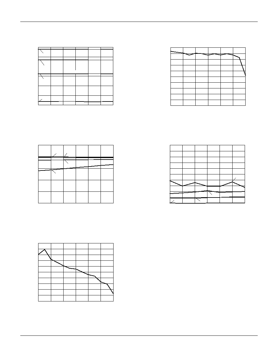
Typical Performance Data
Insertion Loss vs. Frequency and
Control Voltage -- AMPS Band
Frequency (GHz)
Loss (dB)
-30
-25
-20
-15
-10
-5
0
0.865
0.875
0.885
0.895
0 V
4 V
8 V
12 V
Input/Output Return Loss vs. Frequency
and Control Voltage -- AMPS Band
Frequency (GHz)
Return Loss (dB)
-35
-30
-25
-20
-15
-10
0.865
0.875
0.885
0.895
0 V
4 V
8 V
12 V
Insertion Loss Flatness vs.
Control Voltage -- AMPS Band
0
4
2
6
8
10
12
Control Voltage (V)
Flatness (dB)
-0.50
-0.45
-0.40
-0.35
-0.30
-0.25
-0.20
-0.15
-0.10
-0.05
0
Phase vs. Frequency and
Control Voltage -- AMPS Band
Frequency (GHz)
Phase (Degrees)
0
1
2
3
4
5
6
7
8
9
10
0.865
0.875
0.885
0.895
0 V
4 V
8 V
12 V
3rd Order Intermod vs. Control Voltage
RF
1
= 0.900 GHz, RF
2
= 0.905 GHz @ 8 dBm
0
4
2
6
8
10
12
Control Voltage (V)
IP3 (dBm)
30
32
34
36
38
40
42
44
46
48
50
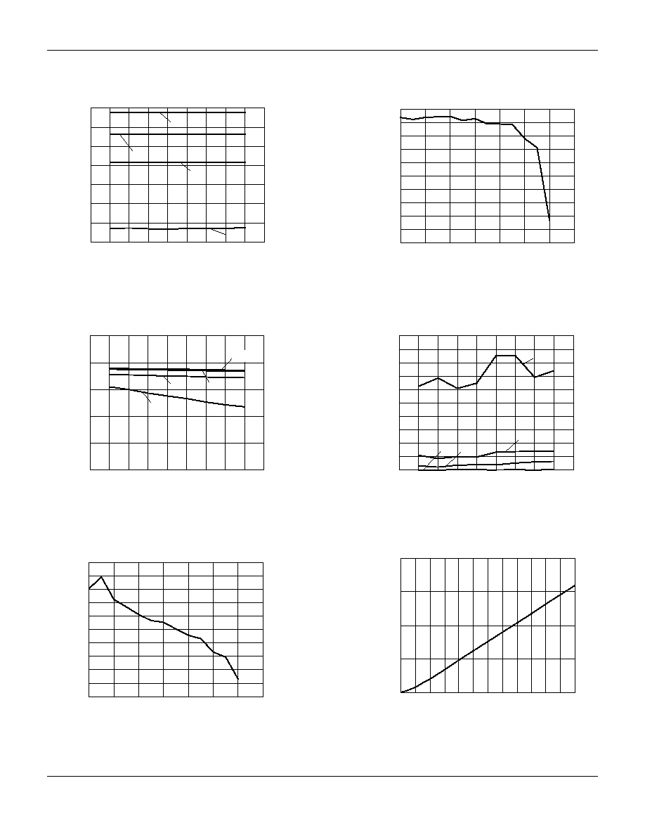
HIP3TM Variable Attenuator for AMPS and GSM Base Stations
AV131-315
Skyworks Solutions, Inc. [781] 376-3000
∑ Fax [781] 376-3100 ∑ Email sales@skyworksinc.com ∑ www.skyworksinc.com
3
Specifications subject to change without notice. 3/03A
Insertion Loss vs. Frequency and
Control Voltage -- GSM Band
Frequency (GHz)
Loss (dB)
-35
-30
-25
-20
-15
-10
-5
0
0.920
0.930
0.940
0.950
0.960
0 V
4 V
8 V
12 V
Input/Output Return Loss vs. Frequency
and Control Voltage -- GSM Band
Frequency (GHz)
Return Loss (dB)
-35
-30
-25
-20
-15
-10
0.920
0.930
0.940
0.950
0.960
0 V
4 V
8 V
12 V
Insertion Loss Flatness vs.
Control Voltage -- GSM Band
0
4
2
6
8
10
14
12
Control Voltage (V)
Flatness (dB)
-0.50
-0.45
-0.40
-0.35
-0.30
-0.25
-0.20
-0.15
-0.10
-0.05
0
Phase vs. Frequency and
Control Voltage -- GSM Band
Frequency (GHz)
Phase (Degrees)
0
1
2
3
4
5
6
7
8
9
10
0.92
0.93
0.94
0.95
0.96
0 V 4 V
8 V
12 V
3rd Order Intermod vs. Control Voltage
RF
1
= 0.900 GHz, RF
2
= 0.905 GHz @ 8 dBm
0
4
2
6
8
10
14
12
Control Voltage (V)
IP3 (dBm)
30
32
34
36
38
40
42
44
46
48
50
Total Current vs. Control Voltage
Control Voltage (V)
Total Current (mA)
0
0.5
1.0
1.5
2.0
0
3
6
9
12
4
Skyworks Solutions, Inc. [781] 376-3000
∑ Fax [781] 376-3100 ∑ Email sales@skyworksinc.com ∑ www.skyworksinc.com
Specifications subject to change without notice. 3/03A
HIP3TM Variable Attenuator for AMPS and GSM Base Stations
AV131-315
Characteristic
Value
RF Input Power
0.5 W CW, 4 W @ 12.5%
Duty Cycle
Control Voltage
15 V
Control Current
50 mA Each Diode
Operating Temperature
-40 to +85∞C
Storage Temperature
-40 to +85∞C
Maximum Reverse Diode Voltage
-10 V
Electrostatic Discharge
+125 V
Absolute Maximum Ratings
Note: Operating this device above any of these parameters may cause
irreversible damage.
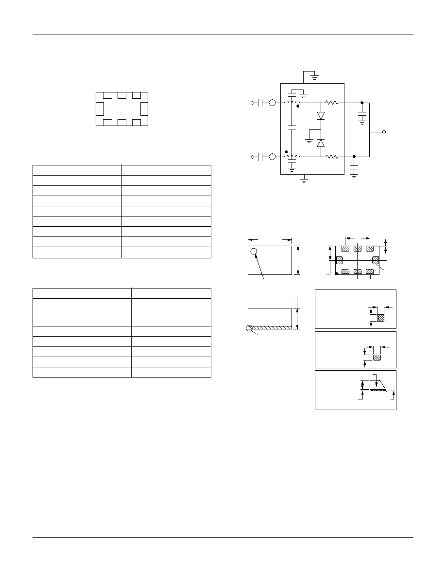
Terminal No.
Terminal Name
A
1
(Pin 1)
IN/OUT
A
2
GND
A
3
IN/OUT
B
1
GND
B
3
GND
C
1
Vcontrol
C
2
GND
C
3
Vcontrol
-315
0.091 (2.32 mm)
± 0.003 (0.091 mm)
0.193 (4.90 mm)
± 0.004 (0.10 mm)
0.126
(3.20 mm)
± 0.004
(0.10 mm)
L
C
L
C
PIN 1 INDICATOR
0.107 (2.740 mm)
± 0.004 (0.100 mm)
0.063
(1.60 mm)
8X 0.004
(0.100 mm)
± 0.001
(0.02 mm)
0.030 (0.775 mm)
± 0.002 (0.050 mm)
0.031 (0.800 mm)
± 0.002 (0.050 mm)
DETAIL
A
DETAIL A
DETAIL C
DETAIL B
0.024 (0.600 mm)
± 0.002 (0.050 mm)
0.031 (0.800 mm)
± 0.002 (0.050 mm)
DETAIL B
DETAIL C
MOLD
SEATING
PLANE
0.078 (2.00 mm)
± 0.002 (0.05 mm)
0.013 (0.32 mm)
± 0.002 (0.4 mm)
B
3
B
1
C
1
C
2
C
3
A
1
A
2
A
3
IN/OUT
GND
IN/OUT
GND
GND
Vcontrol
Vcontrol
GND
AV131
Pin Out (Bottom View)
Vcontrol
CONTROL
VOLTAGE
10 pF
10 pF
10 pF
Vcontrol
RF
IN/OUT
RF
IN/OUT
10 pF
Connection Diagram