Skyworks Solutions, Inc. [978] 241-7000
∑
Fax [978] 241-7906
∑
Email sales@skyworksinc.com
∑
www.skyworksinc.com
1
Specifications subject to change without notice. 8/01A
Silicon Step Recovery Diode Chips
Features
For Frequency Multiplying and Pulse
Shaping
Fast Transition Time for Multiplication to
18 GHz
Long Carrier Lifetime for Input Frequencies
Below 50 MHz
Rugged, Passivated Chip Design
CVB1031 and CVB1151
Characteristic
Value
Reverse Voltage (V
R
)
Breakdown Voltage
Forward Current (I
F
)
100 mA
Power Dissipation (P
D
) @ 25∞C
250 mW
Operating Temperature (T
OP
)
-55 to +150∞C
Storage Temperature (T
ST
)
-65 to +200∞C
Absolute Maximum Ratings
Electrical Characteristics at 25∞C
1. Breakdown voltage specified at 10
µ
A.
2. Capacitance specified at 1 MHz.
3. Carrier lifetime specified at 10 mA.
4. Transition time specified at V
R
= 10 V and I
F
= 10 mA.
5. Cutoff frequency calculated from C
J
@ 6 V and R
S
at 100 mA, 100 MHz.
Breakdown
Carrier Transition Cutoff
Input
Outut
Part Voltage
C
J
@ 6 V
C
J
@ 0 V
Lifetime
Time
Frequency Frequency Frequency
Outline
Number
(V)
(pF)
(pF)
(nS)
(pS)
(GHz)
(MHz)
(GHz)
Drawing
Min.
Min.
Max.
Typ.
Min.
Max.
Min.
Typ.
Typ.
CVB1031-000
30
0.25
0.5
0.5
20
100
300
50≠1000
5≠12
150-801
CVB1151-000
15
0.25
0.5
0.4
10
70
300
100≠3000
9≠18
150-806
Description
Alpha's product line of silicon step recovery diode chips are
designed for use in high order frequency multiplier, comb
generator and pulse shaping applications. These mesa
designed chips have a small outline (12 x 12 mils nominal)
and are fully passivated resulting in low leakage current and
high reliability. The CVB1031-000 may be used at input
frequencies below 50 MHz and will generate harmonics
beyond 12 GHz. The CVB1151-000 may be used at input
frequencies below 100 MHz and will generate harmonics
beyond 18 GHz.

Silicon Step Recovery Diode Chips
CVB1031 and CVB1151
2
Skyworks Solutions, Inc. [978] 241-7000
∑
Fax [978] 241-7906
∑
Email sales@skyworksinc.com
∑
www.skyworksinc.com
Specifications subject to change without notice. 8/01A
ANODE
METALIZED
GOLD DOT
SILICON
CATHODE METALIZED BACK
CONTACT GOLD
0.004 (0.127 mm) MIN.
0.006 (0.152 mm) MAX.
0.010 (0.251 mm) MIN.
0.014 (0.356 mm) MAX. SQ.
150-801:
0.002 (0.051 mm) MIN.
150-806:
0.0011 (0.028 mm) MIN.
Chip
Bonding Pad
Chip Size (In.)
Style
Nominal (In.)
Min.
Max.
150-801
0.002 (Min.)
0 .010
0.014
150-806
0.0011 (Min.)
0 .010
0.014
Outline Drawing
Parameter
CVB1031-000
CVB1151-000
Units
IS
3E-17
3E-17
A
R
S
0.12
0.13
N
1.02
1.03
-
TT
2E-8
1E-8
s
C
J0
0.20
0.30
pF
C
P
0.31
0.25
pF
M
0.70
1.00
-
E
G
0.69
0.69
eV
XTI
2
2
-
F
C
0.50
0.50
-
B
V
30
15
V
I
BV
1.00E-05
1.00E-05
A
V
J
1
2
V
SPICE Model
SPICE model parameters extracted from measured values may not reflect
exact electronic or physical properties. See application note APN1004.
DIODE
Varactor_Diode
AREA = 1
MODEL = Diode_Model
MODE = nonlinear
RES
R
S
R = R
S
CAP
C
P
C = C
P
PORT
P_anode
port = 1
PORT
P_Cathode
port = 2
DIODEM
Diode_Model
I
S
= 1.00e-14
0.5e-12
R
S
= 0
N = 1
T
T
= 0
C
JO
= C
JO
M = M
V
J
= V
J
E
G
= 1.11
1.43
X
TI
= 3
2
K
F
=0
A
F
=1
F
C
= 0.5
B
V
= 0
I
BV
= 1e-3
I
SR
= 0
N
R
= 2
I
KF
= 0
N
BV
= 1
I
BVL
= 0
N
BVL
= 1
T
BV1
= 0
T
NOM
= 27
F
FE
= 1
C
V
=
+ C
P
1+
C
J0
M
V
R
V
J
0
10
20
30
Capacitance (pF)
Reverse Voltage (V)
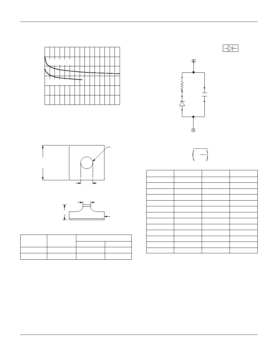
Capacitance vs. Reverse Voltage
0
0.1
0.2
0.3
0.4
0.5
0.6
CVB1151-000
CVB1031-000
Typical Performance Data

