 | ÐлекÑÑоннÑй компоненÑ: CX77107 | СкаÑаÑÑ:  PDF PDF  ZIP ZIP |
Microsoft Word - 101782a.doc
Skyworks Solutions, Inc., Proprietary Information
1
101782A
781] 376-7000 · FAX [781] 376-3100 · SALES@SKYWORKSINC.COM · WWW.SKYWORKSINC.COM
JULY 3, 2003
DATA SHEET
DATA SHEET
DATA SHEET
DATA SHEET
CX77107: PA Module for CDMA / PCS (18501910 MHz)
APPLICATIONS
APPLICATIONS
APPLICATIONS
APPLICATIONS
·
Personal Communications Services
(PCS)
·
Wireless local loop (WLL)
DISTINGUISHING FEATU
DISTINGUISHING FEATU
DISTINGUISHING FEATU
DISTINGUISHING FEATURES
RES
RES
RES
·
Low voltage positive bias supply
(3.2 V to 4.2 V)
·
Good linearity
·
High efficiency
·
Large dynamic range
·
10-pin package
4 mm x 4 mm x 1.5 mm
·
Power down control
·
Low power-state control
·
InGaP
·
IS95/CDMA2000
·
Full U.S. PCS coverage
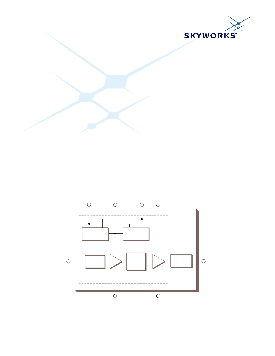
The CX77107 Power Amplifier Module (PAM) is a fully matched 10-pin surface mount
module developed for Personal Communications Service (PCS) and Wireless Local Loop
(WLL) applications. This small and efficient Power Amplifier packs full 18501910 MHz
bandwidth coverage into a single compact package. The CX77107 meets the stringent
spectral linearity requirements of Code Division Multiple Access (CDMA) PCS transmission,
with high power added efficiency for power output of up to 28 dBm. A low current (VCONT)
pin is provided to improve efficiency for the low RF power range of operation.
The single Gallium Arsenide (GaAs) Microwave Monolithic Integrated Circuit (MMIC) contains
all active circuitry in the module. The MMIC contains on-board bias circuitry, as well as
input and interstage matching circuits. The output match is realized off-chip within the
module package to optimize efficiency and power performance into a 50 W load. This
device is manufactured with Skyworks' GaAs Heterojunction Bipolar Transistor (HBT)
process that provides for all positive voltage DC supply operation while maintaining high
efficiency and good linearity. Primary bias to the CX77107 is supplied directly from a three-
cell nickel cadmium, a single-cell lithium ion, or other suitable battery with an output in the
3 to 4 volt range. Power down is accomplished by setting the voltage on the low current
reference pin to zero volts. No external supply side switch is needed as typical "off" leakage
is a few microamperes with full primary voltage supplied from the battery.
MMIC
MODULE
(8) RF OUT
VCC1
VCC2
VREF
(5)
(1)
(10)
(3, 6, 7, 9)
GND
VCONT
(4)
(3, 6, 7, 9)
GND
RF IN (2)
DA
Driver
Stage Bias
Power
Stage Bias
Input
Match
Inter
Stage
Match
PA
Output
Match
101782_001
Figure
Figure
Figure
Figure 1
1
1
1. Functional Block Diagram
. Functional Block Diagram
. Functional Block Diagram
. Functional Block Diagram
Data Sheet · CX77107
PA Module for CDMA / PCS (18501910 MHz)
2
Skyworks Solutions, Inc., Proprietary Information
JULY 3, 2003
781] 376-7000 · FAX [781] 376-3100 · SALES@SKYWORKSINC.COM · WWW.SKYWORKSINC.COM
101782A
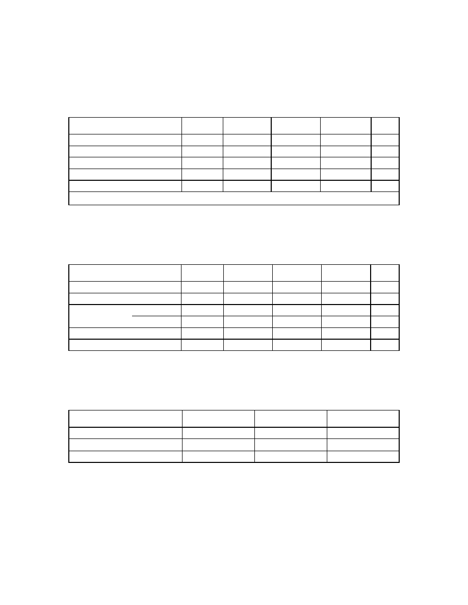
Electrical Specifications
Electrical Specifications
Electrical Specifications
Electrical Specifications
The following tables list the electrical characteristics of the
CX77107 Power Amplifier.
Table 1
lists the absolute maximum
ratings, while
Table 2
shows the recommended operating
conditions to achieve the performance characteristics listed in
Table 4
.
Table 3
presents a truth table for the power ranges.
Table
Table
Table
Table 1
1
1
1. Absolute Maximum Ratings
. Absolute Maximum Ratings
. Absolute Maximum Ratings
. Absolute Maximum Ratings
(1)
(1)
(1)
(1)
Parameter
Parameter
Parameter
Parameter Symbol
Symbol
Symbol
Symbol Minimum
Minimum
Minimum
Minimum Nominal
Nominal
Nominal
Nominal Maximum
Maximum
Maximum
Maximum Unit
Unit
Unit
Unit
RF Input Power
P
IN
--
0.0
7.0
dBm
Supply Voltage
V
CC
--
3.4
6.0
Volts
Reference Voltage
V
REF
--
3.0
3.1
Volts
Case Operating Temperature
T
C
30
25
+110
°C
Storage Temperature
T
STG
55
--
+125
°C
(1)
No damage assuming only one parameter is set at limit at a time with all other parameters set at or below nominal value.
Table
Table
Table
Table 2
2
2
2. Recommended Operating Conditi
. Recommended Operating Conditi
. Recommended Operating Conditi
. Recommended Operating Conditions
ons
ons
ons
Parameter
Parameter
Parameter
Parameter Symbol
Symbol
Symbol
Symbol Minimum
Minimum
Minimum
Minimum Nominal
Nominal
Nominal
Nominal Maximum
Maximum
Maximum
Maximum Unit
Unit
Unit
Unit
Supply Voltage
V
CC
3.2
3.4
4.2
Volts
Reference Voltage
V
REF
2.95
3.0
3.05
Volts
Low Mode
V
CONT
2.5 -- 3.0
Volts
Control voltage
High Mode
V
CONT
0.0 -- 0.5
Volts
Operating Frequency
F
O
1850.0
1880.0
1910.0
MHz
Case Operating Temperature
T
C
30
+25
+85
°C
Table
Table
Table
Table 3
3
3
3. Power Range Truth Table
. Power Range Truth Table
. Power Range Truth Table
. Power Range Truth Table
Power Mode
Power Mode
Power Mode
Power Mode
V
V
V
V
REF
REF
REF
REF
V
V
V
V
CONT
CONT
CONT
CONT
Range
Range
Range
Range
High Power
3.0 V
0.0 V0.5 V
16 dBm28 dBm
Low Power
3.0 V
2.5 V3.0 V
16 dBm
Shut Down
0.0 V
0.0 V
--
PA Module for CDMA / PCS (18501910 MHz)
Data Sheet · CX77107
Skyworks Solutions, Inc., Proprietary Information
3
101782A
781] 376-7000 · FAX [781] 376-3100 · SALES@SKYWORKSINC.COM · WWW.SKYWORKSINC.COM
JULY 3, 2003
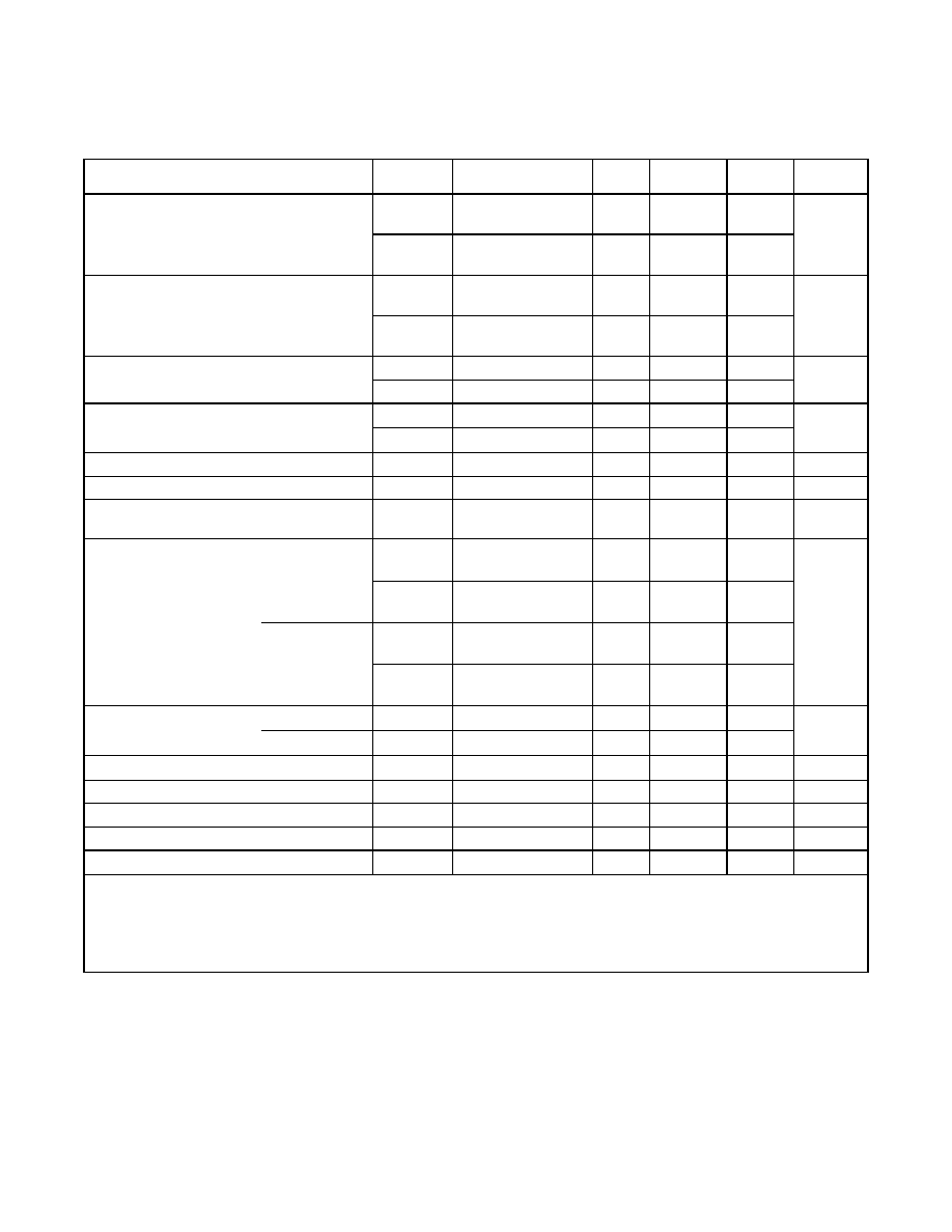
Ta
Ta
Ta
Table
ble
ble
ble 4
4
4
4. Electrical Specifications for CDMA Nominal Operating Conditions
. Electrical Specifications for CDMA Nominal Operating Conditions
. Electrical Specifications for CDMA Nominal Operating Conditions
. Electrical Specifications for CDMA Nominal Operating Conditions
(1)
(1)
(1)
(1)
Characteristics
Characteristics
Characteristics
Characteristics Symbol
Symbol
Symbol
Symbol Condition
Condition
Condition
Condition Min.
Min.
Min.
Min. Typical
Typical
Typical
Typical Max.
Max.
Max.
Max. Unit
Unit
Unit
Unit
G
LOW
V
CONT
2.5 V
P
O
= 16 dBm
22.0 24.0 26.5
Gain conditions
Digital Mode
G
HIGH
V
CONT
0.5 V
P
O
= 28 dBm
26.5 28.0 30.0
dB
PAE
LOW
V
CONT
2.5 V
P
O
= 16 dBm
7.5 9.0 --
Power Added Efficiency
Digital Mode
PAE
HIGH
V
CONT
0.5 V
P
O
= 28 dBm
37.0 39.0 --
%
I
CC_LOW
P
O
= 16 dBm
--
125
150
Total Supply current
I
CC_HIGH
P
O
= 28 dBm
--
475
500
mA
I
Q_LOW
V
CONT
2.5 V
-- 50 --
Quiescent current
I
Q_HIGH
V
CONT
0.5 V
-- 90 --
mA
Reference Current
I
REF
--
--
6.0
--
mA
Control Current
I
CTRL
V
CONT
= 2.5 V
--
140
--
mA
Total Supply current in Power-down Mode
I
PD
V
CC
= 3.4V
V
REF
= 0 V
-- 3.0 5.0 mA
ACP1
LOW
V
CONT
2.5 V
P
O
16 dBm
-- 48.0 45.0
1.25 MHz offset
ACP1
HIGH
V
CONT
0.5 V
P
O
28 dBm
-- 50.0 48.0
ACP3
LOW
V
CONT
2.5 V
P
O
16 dBm
-- 73.0 58.0
Adjacent Channel Power
(2) (3)
2.25 MHz offset
ACP3
HIGH
V
CONT
0.5 V
P
O
28 dBm
-- 58.5 56.5
dBc
Second F
O
2
P
O
28 dBm
-- 40.0 35.0
Harmonic Suppression
Third F
O
3
P
O
28 dBm
-- 55.0 40.0
dBc
Noise Power in RX Band 1930-1990 MHz
RxBN
P
O
28 dBm
-- 138.0 137.0
dBm/Hz
Noise Figure
NF
--
--
4.0
5.0
dB
Input Voltage Standing Wave Ratio (VSWR)
VSWR
--
--
--
2.0:1
--
Stability (Spurious output)
S
5:1 VSWR All phases
--
--
70.0
dBc
Ruggedness No damage
(4)
Ru
P
O
28 dBm
10:1 -- -- VSWR
(1)
V
CC
= +3.4 V, V
REF
= +3.0 V, Freq = 1880 MHz, T
C
= 25 °C, unless otherwise specified
(2)
ACP is specified per IS95 as the ratio of the total in-band power (1.23 MHz BW) to adjacent power in a 30 kHz BW.
(3)
CDMA2000 is configured as DCCH = 9600, SCHO = 9600, PCH (Walsh 0) = 3.75 dB, and Peak-to-Average Ratio (CCDF = 1%) = 4.5 dB. For CDMA2000, 0.5 dB
back-off in output power is required.
(4)
All phases, time = 10 seconds.
Data Sheet · CX77107
PA Module for CDMA / PCS (18501910 MHz)
4
Skyworks Solutions, Inc., Proprietary Information
JULY 3, 2003
781] 376-7000 · FAX [781] 376-3100 · SALES@SKYWORKSINC.COM · WWW.SKYWORKSINC.COM
101782A
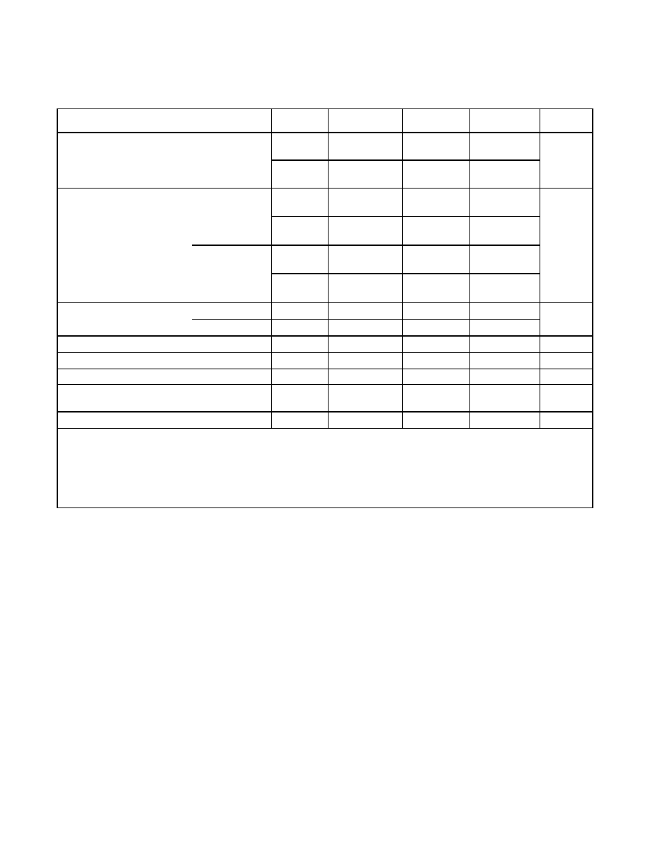
Table
Table
Table
Table 5
5
5
5. Electrical Specifications for CDMA Recommended Operating Conditions
. Electrical Specifications for CDMA Recommended Operating Conditions
. Electrical Specifications for CDMA Recommended Operating Conditions
. Electrical Specifications for CDMA Recommended Operating Conditions
(1)
(1)
(1)
(1)
Characteristics
Characteristics
Characteristics
Characteristics Symbol
Symbol
Symbol
Symbol Condition
Condition
Condition
Condition Minimum
Minimum
Minimum
Minimum Maximum
Maximum
Maximum
Maximum Unit
Unit
Unit
Unit
G
LOW
V
CONT
2.5 V
P
O
= 16 dBm
21.0 29.5
Gain conditions
Digital Mode
G
HIGH
V
CONT
0.5 V
P
O
= 28 dBm
24.5 33.0
dB
ACP1
LOW
V
CONT
2.5 V
P
O
16 dBm
-- 44
1.25 MHz offset
ACP1
HIGH
V
CONT
0.5 V
P
O
28 dBm
-- 44
ACP3
LOW
V
CONT
2.5 V
P
O
16 dBm
-- 56
Adjacent Channel Power
(2) (3) (4)
2.25 MHz offset
ACP3
HIGH
V
CONT
0.5 V
P
O
28 dBm
-- 56
dBc
Second F
O
2
P
O
28 dBm
-- 30
Harmonic Suppression
Third F
O
3
P
O
28 dBm
-- 40
dBc
Noise Power in RX Band 1840-1895 MHz
RxBN
P
O
28 dBm
-- 136.0
dBm/Hz
Noise Figure
NF
--
--
7.0
dB
Input Voltage Standing Wave Ratio (VSWR)
VSWR
--
--
2.5:1
--
Stability (Spurious output)
S
5:1 VSWR
All phases
-- 70.0
dBc
Ruggedness No damage
(5)
Ru
P
O
28 dBm
10:1 --
VSWR
(1)
Per Table 2, unless otherwise specified.
(2)
ACP is specified per IS95 as the ratio of the total in-band power (1.23 MHz BW) to adjacent power in a 30 kHz BW.
(3)
CDMA2000 is configured as DCCH = 9600, SCHO = 9600, PCH (Walsh 0) = 3.75 dB, and Peak-to-Average Ratio (CCDF = 1%) = 4.5 dB. For CDMA2000, 0.5 dB
back-off in output power is required.
(4)
Worst case ACPR is 43dBc at +85 °C, V
CC
= 3.2 V.
(5)
All phases, time = 10 seconds.
PA Module for CDMA / PCS (18501910 MHz)
Data Sheet · CX77107
Skyworks Solutions, Inc., Proprietary Information
5
101782A
781] 376-7000 · FAX [781] 376-3100 · SALES@SKYWORKSINC.COM · WWW.SKYWORKSINC.COM
JULY 3, 2003
Characterization Data
Characterization Data
Characterization Data
Characterization Data
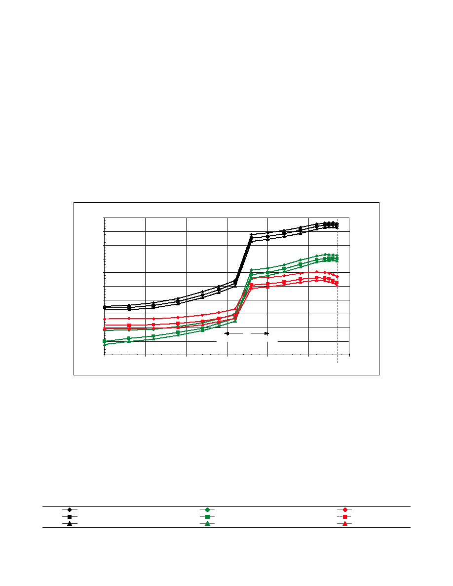
The graphs from
Figure 2
through
Figure 10
illustrate the
characteristics of a typical CX77107 power amplifier designed for
operation in the PCS frequency band (18501910 MHz). This
amplifier was selected by characterizing a group of devices and
choosing a part with average electrical performance for both
nominal and the full range of recommended operating conditions,
including worst case limits.
The graphs illustrate the digital signal characteristics of the
CX77107. Shown are power sweep characteristics for key
performance parameters over temperature and frequency, up to
28.5 dBm output power. The data was taken up to and including
16 dBm output power with the bias mode control pin setting of
V
CONT
= 2.5 volts. Beyond 16 dBm output power, the V
CONT
was set
to 0 volts.
21
22
23
24
25
26
27
28
29
30
31
0
5
10
15
20
25
30
Output Power (dBm)
Gain (dB)
V
REF
= 3.0 V V
CC
= 3.4 V
30 °C
28.5 dBm
+25 °C
+85 °C
V
CONT
> 2.5 V V
CONT
< 0.5 V
101782_010
Figure
Figure
Figure
Figure 2
2
2
2. Digital Mode Gain vs. Output Power
. Digital Mode Gain vs. Output Power
. Digital Mode Gain vs. Output Power
. Digital Mode Gain vs. Output Power
1880 @ +25 °C
1850 @ 30 °C
1850 @ +25 °C
1850 @ +85 °C
1880 @ 30 °C
1880 @ +85 °C
1910 @ 30 °C
1910 @ +25 °C
1910 @ +85 °C
Legend
Document Outline