 | –≠–ª–µ–∫—Ç—Ä–æ–Ω–Ω—ã–π –∫–æ–º–ø–æ–Ω–µ–Ω—Ç: CX77301 | –°–∫–∞—á–∞—Ç—å:  PDF PDF  ZIP ZIP |

Skyworks Solutions, Inc. Proprietary Information
1
100956E
[781] 376-7000 ∑ FAX [781] 376-3100 ∑ SALES@SKYWORKSINC.COM ∑
WWW.SKYWORKSINC.COM
SEPTEMBER 19, 2003
DATA SHEET
DATA SHEET
DATA SHEET
DATA SHEET
CX77301: PA Module Dual-band EGSM900 DCS1800 / GPRS
APPLICATIONS
APPLICATIONS
APPLICATIONS
APPLICATIONS
∑
Dual-band cellular handsets
encompassing
-
Class 4 EGSM900,
-
Class 1 DCS1800
-
up to Class 10 GPRS multi-slot
operation.
FEATURES
FEATURES
FEATURES
FEATURES
∑
High efficiency
-
EGSM 55%
-
DCS 50%
∑
Input/output matching
-
50
internal
∑
Small outline 9.1 mm x 11.6 mm
∑
Low profile 1.5 mm maximum
∑
Low APC current 10
µA typical
The CX77301 is a dual-band Power Amplifier Module (PAM) designed in a compact form
factor for Class 4 EGSM900 and Class 1 DCS1800 operation that also supports multi-slot
transmission for Class 10 General Packet Radio Service (GPRS) operation.
The module consists of an EGSM900 PA block, a DCS1800 PA block, impedance matching
circuitry for 50
input and output impedances, and bias control circuitry. Two separate
Heterojunction Bipolar Transistor (HBT) PA blocks are fabricated on a single Gallium
Arsenide (GaAs) die. One PA block operates in the EGSM900 band and the other PA block
supports the DCS1800 band. Optimized for lithium ion battery operation, both PA blocks
share common power supply pins to distribute current. A custom CMOS integrated circuit
provides the internal interface circuitry, including a current amplifier that minimizes the
required power control current (I
APC
) to 10
µA, typical. The GaAs die, the Silicon (Si) die, and
passive components are mounted on a multi-layer laminate substrate. The assembly is
encapsulated with plastic overmold.
The RF input and output ports are internally matched to 50
to reduce the number of
external components for a dual-band design. Extremely low leakage current (2
µA, typical)
of the dual PA module maximizes handset standby time. The CX77301 also contains band-
select switching circuitry to select EGSM (logic 0) or DCS (logic 1) as determined from the
Band Select (BS) signal. In the Functional Block Diagram shown below, the BS pin selects
the PA output (DCS OUT or EGSM OUT) while the Analog Power Control (APC) controls the
level of output power.
CMOS
Bias
Controller
EGSM IN
EGSM OUT
DCS IN
DCS OUT
Power Control
Band Select
HBT
Match
Match
Match
Match
100956_001
Figure
Figure
Figure
Figure 1
1
1
1. Functional Block Diagram
. Functional Block Diagram
. Functional Block Diagram
. Functional Block Diagram

Data Sheet ∑ CX77301
PA Module for Dual-band EGSM900 DCS1800 / GPRS
2
Skyworks Solutions, Inc. Proprietary Information
SEPTEMBER 19, 2003
[781] 376-7000 ∑ FAX [781] 376-3100 ∑ SALES@SKYWORKSINC.COM ∑
WWW.SKYWORKSINC.COM
100956E
ELECTRICAL SPECIFICA
ELECTRICAL SPECIFICA
ELECTRICAL SPECIFICA
ELECTRICAL SPECIFICATIONS
TIONS
TIONS
TIONS
The following tables list the electrical characteristics of the
CX77301 Power Amplifier.
Table 1
lists the absolute maximum
ratings and
Table 2
shows the recommended operating
conditions.
Table 3
shows the electrical characteristics of the
CX77301 for EGSM and DSC modes. A typical CX77301
application diagram appears in
Figure 2
.
The CX77301 is a static-sensitive electronic device and should
not be stored or operated near strong electrostatic fields. Detailed
ESD precautions along with information on device dimensions,
pin descriptions, packaging and handling can be found in later
sections of this data sheet.
Table
Table
Table
Table 1
1
1
1. Absolute Maximum Ratings
. Absolute Maximum Ratings
. Absolute Maximum Ratings
. Absolute Maximum Ratings
Parameter
Parameter
Parameter
Parameter
Minimum
Minimum
Minimum
Minimum
Maximum
Maximum
Maximum
Maximum
Unit
Unit
Unit
Unit
Input power (P
IN
)
--
15
dBm
Supply voltage (V
CC
), standby, V
APC
0.3 V
--
7
V
Control voltage (V
APC
)
≠0.5
V
CC_MAX
≠ 0.2
(See
Table 3
)
V
Storage Temperature
≠55
+100
∞C
Table
Table
Table
Table 2
2
2
2. CX77301 Recommended Operating C
. CX77301 Recommended Operating C
. CX77301 Recommended Operating C
. CX77301 Recommended Operating Conditions
onditions
onditions
onditions
Parameter
Parameter
Parameter
Parameter
Minimum
Minimum
Minimum
Minimum
Typical
Typical
Typical
Typical
Maximum
Maximum
Maximum
Maximum
Unit
Unit
Unit
Unit
Supply Voltage (V
CC
)
2.9
3.5
4.8 V
(1)
V
Supply Current (I
CC
)
0
--
2.5
(1)
A
Operating Case Temperature (T
CASE
)
1-Slot (12.5% duty cycle)
≠20
--
100
2-Slot (25% duty cycle)
≠20
--
90
3-Slot (37.5% duty cycle)
≠20
--
75
4-Slot ( 50% duty cycle)
≠20
--
60
∞C
(1)
For charging conditions with V
CC
> 4.8 V, derate I
CC
linearly down to 0.5 A max at V
CC
= 5.5 V

PA Module for Dual-band EGSM900 DCS1800 / GPRS
Data Sheet ∑ CX77301
Skyworks Solutions, Inc. Proprietary Information
3
100956E
[781] 376-7000 ∑ FAX [781] 376-3100 ∑ SALES@SKYWORKSINC.COM ∑
WWW.SKYWORKSINC.COM
SEPTEMBER 19, 2003
T
T
T
Table
able
able
able 3
3
3
3. CX77301 Electrical Specifications
. CX77301 Electrical Specifications
. CX77301 Electrical Specifications
. CX77301 Electrical Specifications(1)
(1)
(1)
(1) (1 of 3)
(1 of 3)
(1 of 3)
(1 of 3)
Parameter
Parameter
Parameter
Parameter
Sy
Sy
Sy
Symbol
mbol
mbol
mbol
Test Condition
Test Condition
Test Condition
Test Condition
Min
Min
Min
Min
Typical
Typical
Typical
Typical
Max
Max
Max
Max
Units
Units
Units
Units
General
General
General
General
Supply Voltage
V
CC
--
2.9
3.5
4.8V
V
Power Control Current
I
APC
--
--
10
100
µA
Leakage Current
I
Q
V
CC
= 4.5 V
V
APC
= 0.3 V
T
CASE
= +25 ∞C
P
IN
≠60 dBm
--
--
5
µA
APC Enable Threshold
V
APCTH
--
200
--
600
mV
APC Enable Switching Delay
SW
Time from V
APC
V
APCTH
until
P
OUT
(P
OUT_FINAL
≠3 dB)
5
8
µs
EGSM Mode (f = 880 to 915 MHz and
EGSM Mode (f = 880 to 915 MHz and
EGSM Mode (f = 880 to 915 MHz and
EGSM Mode (f = 880 to 915 MHz and P
P
P
P
IN
IN
IN
IN
= 6 to 12 dBm)
= 6 to 12 dBm)
= 6 to 12 dBm)
= 6 to 12 dBm)
Frequency Range
f
--
880
--
915
MHz
Input Power
P
IN
--
6
--
12
dBm
Analog Power Control Voltage
V
APC
P
OUT
= 32 dBm
1.2
1.7
2.1
V
Power Added Efficiency
PAE
V
CC
= 3.5 V
P
OUT
34.5 dBm
V
APC
2.0 V
pulse width = 577
µs
duty cycle = 1:8
T
CASE
= +25 ∞C
50
55
--
%
2nd to 13th Harmonics
2f0 to 13f0
BW = 3 MHz
5 dBm
P
OUT
35 dBm
--
--
≠7
dBm
P
OUT
V
CC
= 3.5 V
V
APC
2.0 V
T
CASE
= +25 ∞C
34.5
35.0
--
P
OUT MAX
V
CC
= 2.9 V
V
APC
2.6 V
T
CASE
= ≠20 ∞C to +100 ∞C
(See
Table 2
for multi-slot)
P
IN
= 6 dBm
32
33
--
Output Power
P
OUT MAX
V
CC
= 4.8 V
V
APC
2.6 V
T
CASE
= ≠20 ∞C to +100 ∞C
(See
Table 2
for multi-slot)
P
IN
= 6 dBm
32
33
--
dBm
Input VSWR
IN
P
OUT
= 5 to 35 dBm, controlled by V
APC
--
1.5:1
2:1
--
Forward Isolation
P
OUT STANDBY
P
IN
= 12 dBm
V
APC
= 0.3 V
--
≠35
≠30
dBm
Time from P
OUT
= ≠10 dBm to
P
OUT
= +5 dBm,
90%
--
5
8
Time from P
OUT
= ≠10 dBm to
P
OUT
= +20 dBm,
90%
--
5
8
Switching Time
RISE
,
FALL
Time from P
OUT
= ≠10 dBm to
P
OUT
= +34.5 dBm,
90%
--
2
4
µs

Data Sheet ∑ CX77301
PA Module for Dual-band EGSM900 DCS1800 / GPRS
4
Skyworks Solutions, Inc. Proprietary Information
SEPTEMBER 19, 2003
[781] 376-7000 ∑ FAX [781] 376-3100 ∑ SALES@SKYWORKSINC.COM ∑
WWW.SKYWORKSINC.COM
100956E
Table 3. CX77301 Electrical Specifications
Table 3. CX77301 Electrical Specifications
Table 3. CX77301 Electrical Specifications
Table 3. CX77301 Electrical Specifications(1)
(1)
(1)
(1) (2 of 3)
(2 of 3)
(2 of 3)
(2 of 3)
Parameter
Parameter
Parameter
Parameter
Symbol
Symbol
Symbol
Symbol
Test Condition
Test Condition
Test Condition
Test Condition
Min
Min
Min
Min
Typical
Typical
Typical
Typical
Max
Max
Max
Max
Units
Units
Units
Units
Spurious
Spur
All combinations of the following parameters:
V
APC
= Controlled
(2)
P
IN
= Min. to Max.
V
CC
= 2.9 V to 4.8 V
Load VSWR = 8:1, all phase angles
No parasitic oscillation > ≠36 dBm
Load Mismatch
Load
All combinations of the following parameters:
V
APC
= Controlled
(2)
P
IN
= Min. to Max.
V
CC
= 2.9 V to 4.8 V
Load VSWR = 10:1, all phase angles
No module damage or permanent
degradation
At f0 + 20 MHz:
RBW = 100 kHz
V
CC
= 3.5 V
5 dBm
P
OUT
34.5 dBm
--
--
≠82
At f0 + 10 MHz:
RBW = 100 kHz
V
CC
= 3.5 V
5 dBm
P
OUT
34.5 dBm
--
--
≠76
Noise Power
P
NOISE
At 1805 to 1880 MHz:
RBW = 100 kHz
V
CC
= 3.5 V
5 dBm
P
OUT
34.5 dBm
--
--
≠90
dBm
Coupling of 2nd and 3rd Harmonic
from the EGSM Band into the DCS
Band
2f0, 3f0
Measured at the DCS output,
≠15 dBm
P
OUT
34 dBm
--
≠25
≠20
dBm
DCS Mode (f = 1710 to 1785 MHz and
DCS Mode (f = 1710 to 1785 MHz and
DCS Mode (f = 1710 to 1785 MHz and
DCS Mode (f = 1710 to 1785 MHz and P
P
P
P
IN
IN
IN
IN
= 5 to 11 dBm)
= 5 to 11 dBm)
= 5 to 11 dBm)
= 5 to 11 dBm)
Frequency Range
f
--
1710
--
1785
MHz
Input Power
P
IN
--
5
--
11
dBm
Analog Power Control Voltage
V
APC
P
OUT
= 29.5 dBm
1.35
1.7
2.1
V
Power Added Efficiency
PAE
V
CC
= 3.5 V
P
OUT
31.5 dBm
V
APC
2.0 V
pulse width = 577
µs
duty cycle = 1:8
T
CASE
= +25 ∞C
45
50
--
%
2nd to 7th Harmonics
2f0 to 7f0
BW = 3 MHz
0 dBm
P
OUT
32 dBm
--
--
≠7
DBm
P
OUT
V
CC
= 3.5 V
V
APC
2.0 V
T
CASE
= +25 ∞C
31.5
32.0
--
P
OUT MAX
V
CC
= 2.9 V
V
APC
2.6 V
T
CASE
= ≠20 ∞C to +100 ∞C
(See
Table 2
for multi-slot)
P
IN
= 5 dBm
29.5
30.5
--
Output Power
P
OUT MAX
V
CC
= 4.8 V
V
APC
2.6 V
T
CASE
= ≠20 ∞C to +100 ∞C
(See
Table 2
for multi-slot)
P
IN
= 5 dBm
29.5
30.5
--
DBm

PA Module for Dual-band EGSM900 DCS1800 / GPRS
Data Sheet ∑ CX77301
Skyworks Solutions, Inc. Proprietary Information
5
100956E
[781] 376-7000 ∑ FAX [781] 376-3100 ∑ SALES@SKYWORKSINC.COM ∑
WWW.SKYWORKSINC.COM
SEPTEMBER 19, 2003
Table 3. CX77301 Electrical Specifications
Table 3. CX77301 Electrical Specifications
Table 3. CX77301 Electrical Specifications
Table 3. CX77301 Electrical Specifications(1)
(1)
(1)
(1) (3 of 3)
(3 of 3)
(3 of 3)
(3 of 3)
Parameter
Parameter
Parameter
Parameter
Symbol
Symbol
Symbol
Symbol
Test Condition
Test Condition
Test Condition
Test Condition
Min
Min
Min
Min
Typical
Typical
Typical
Typical
Max
Max
Max
Max
Units
Units
Units
Units
Input VSWR
IN
P
OUT
= 0 to 32 dBm, controlled by V
APC
--
--
2:1
--
Forward Isolation
P
OUT STANDBY
P
IN
= 10.5 dBm
V
APC
= 0.3 V
--
≠40
≠35
dBm
Time from P
OUT
= ≠10 dBm to
P
OUT
= 0 dBm,
90%
--
10
12
Time from P
OUT
= ≠10 dBm to
P
OUT
= +20 dBm,
90%
--
5
8
Switching Time
RISE
,
FALL
Time from P
OUT
= ≠10 dBm to
P
OUT
= +31.5 dBm,
90%
--
2
5
µs
Spurious
Spur
All combinations of the following parameters:
V
APC
= Controlled
(3)
P
IN
= min. to max.
V
CC
= 2.9 V to 4.8 V
Load VSWR = 8:1, all phase angles
No parasitic oscillation > ≠36 dBm
Load Mismatch
Load
All combinations of the following parameters:
V
APC
= Controlled
(3)
P
IN
= Min. to Max.
V
CC
= 2.9 V to 4.8 V
Load VSWR = 10:1, all phase angles
No module damage or permanent
degradation
At f0 + 20 MHz:
RBW = 100 kHz
V
CC
= 3.5 V
0 dBm
P
OUT
31.5 dBm
--
--
≠80
Noise Power
P
NOISE
At 925 to 960 MHz:
RBW = 100 kHz
V
CC
= 3.5 V
0 dBm
P
OUT
31.5 dBm
--
--
≠95
dBm
(1)
Unless specified otherwise: T
CASE
= ≠20 ∞C to maximum operating temperature (see
Table 2
), RL = 50
, pulsed operation with pulse width 2308 µs, duty cycle
4:8, V
CC
= 2.9 V to 4.8 V
(2)
I
C
= 0A to xA, where x = current at P
OUT
= 34.5 dBm, 50
load, and V
CC
= 3.5 V.
(3)
l
C
= 0A to xA, where x = current at P
OUT
= 32.0 dBm, 50
load, and V
CC
= 3.5 V.

Data Sheet ∑ CX77301
PA Module for Dual-band EGSM900 DCS1800 / GPRS
6
Skyworks Solutions, Inc. Proprietary Information
SEPTEMBER 19, 2003
[781] 376-7000 ∑ FAX [781] 376-3100 ∑ SALES@SKYWORKSINC.COM ∑
WWW.SKYWORKSINC.COM
100956E
BS in from Baseband
EGSM IN
DCS / PCS IN
APC from PAC
10 pF
10 pF
33 pF
DCS / PCS OUT
EGSM OUT
2
4
10
12
16
14
VCC2 output stages
VCC1 drivers
8
6
100 pF
Note 1
10 uF
electrolytic
Vbat
APC IN
Note 2
Note 2
Note 1 - Should be very close to PA module
Note 2 - Optional depending on PAC circuit
10 nF
Note 1
100956_003
C X 7 7 3 0 1
Figure
Figure
Figure
Figure 2
2
2
2. Typical CX77301 Application
. Typical CX77301 Application
. Typical CX77301 Application
. Typical CX77301 Application

PA Module for Dual-band EGSM900 DCS1800 / GPRS
Data Sheet ∑ CX77301
Skyworks Solutions, Inc. Proprietary Information
7
100956E
[781] 376-7000 ∑ FAX [781] 376-3100 ∑ SALES@SKYWORKSINC.COM ∑
WWW.SKYWORKSINC.COM
SEPTEMBER 19, 2003
PACKAGE DIMENSIONS A
PACKAGE DIMENSIONS A
PACKAGE DIMENSIONS A
PACKAGE DIMENSIONS AND PIN DESCRIPTIONS
ND PIN DESCRIPTIONS
ND PIN DESCRIPTIONS
ND PIN DESCRIPTIONS
Figure 3
displays the dimensions of the 16-pin leadless CX77301
dual-band PAM.
Figure 4
provides a recommended phone board
layout footprint for the PAM to help the designer attain optimum
thermal conductivity, good grounding, and minimum RF
discontinuity for the 50 ohm terminals.
Figure 5
shows the device
pin configuration, and
Table 4
describes the pin names and
signals.
BOTTOM VIEW
SIDE VIEW
TOP VIEW
SOLDER MASK EDGES
0.1 A B C
2X R0.3
2X R0.2
1.145
0.145
0.9
0.76
0.96
METAL PAD EDGES
0.05 A B C
DETAIL
A
PAD
SCALE: 2X
3X THIS ROTATION
3X ROTATED 180∞
5X ROTATED 90∞ CW
5X ROTATED 90∞ CCW
4X R0.2
SOLDER MASK OPENING
0.15 A B C
(3.33)
METAL PAD - PIN 1
( / 0.15)
SOLDER MASK OPENING
( / 0.30)
(4.43)
4X 1.905
2X 3.514
2X 2.261
4X 1.905
4X 3.81
(0.465)
A
MCM SUBSTRATE
MOLD
A
A
0.025
1.5±0.1
0.08
0.10 A B C
9.14
C
B
11.64
PIN 1 INDICATOR
NOTES: unless otherwise specified
1. ALL DIMENSIONS ARE IN MILLIMETERS.
2. DIMENSIONING AND TOLERANCING IN ACCORDANCE WITH ASME Y14.5M≠1994
3. SEE APPLICABLE BONDING DIAGRAM AND DEVICE ASSEMBLY DRAWING FOR DIE AND COMPONENT PLACEMENT.
4. PADS ARE METAL DEFINED. THE CENTER PAD IS SOLDER MASK DEFINED.
100956_004
Figure
Figure
Figure
Figure 3
3
3
3. CX77301 Package Dimensions
. CX77301 Package Dimensions
. CX77301 Package Dimensions
. CX77301 Package Dimensions≠
≠
≠
≠16
16
16
16----pin Module (All Vi
pin Module (All Vi
pin Module (All Vi
pin Module (All Views)
ews)
ews)
ews)

Data Sheet ∑ CX77301
PA Module for Dual-band EGSM900 DCS1800 / GPRS
8
Skyworks Solutions, Inc. Proprietary Information
SEPTEMBER 19, 2003
[781] 376-7000 ∑ FAX [781] 376-3100 ∑ SALES@SKYWORKSINC.COM ∑
WWW.SKYWORKSINC.COM
100956E
0.86
1.42
5.00
PIN 1
PIN
16
3.20 9.8
1.905
12.3
STENCIL APERTURE
TOP VIEW
APPROACH 1
Component
Outline
Common Ground Pad
0.762
1.32
9.70
1.905 TYP
0.250
12.20
METALLIZATION
TOP VIEW
Thermal Via Array
/ 0.3 mm on 0.8 mm pitch
Additional vias will improve
thermal performance.
NOTE: Thermal vias should be
tented and filled with solder mask,
30≠35 µm Cu plating recommended.
o
SOLDER MASK OPENING
TOP VIEW
12.3
7
4X 0.82
1.91 TYP
9.8
1.42
0.05 ALL AROUND
0.86
4.5
1.42
0.86
1.8
1
0.3
9.8
1.91
12.3
STENCIL APERTURE
TOP VIEW
APPROACH 2
Component
Outline
Component
Outline
Component
Outline
PIN 1
PIN
16
PIN 1
PIN
16
PIN 1
PIN
16
100956_014
Figure
Figure
Figure
Figure 4
4
4
4. Phone Board Layout Footprint for 9.1 mm x 11.6 mm Package
. Phone Board Layout Footprint for 9.1 mm x 11.6 mm Package
. Phone Board Layout Footprint for 9.1 mm x 11.6 mm Package
. Phone Board Layout Footprint for 9.1 mm x 11.6 mm Package

PA Module for Dual-band EGSM900 DCS1800 / GPRS
Data Sheet ∑ CX77301
Skyworks Solutions, Inc. Proprietary Information
9
100956E
[781] 376-7000 ∑ FAX [781] 376-3100 ∑ SALES@SKYWORKSINC.COM ∑
WWW.SKYWORKSINC.COM
SEPTEMBER 19, 2003
GND
EGSMIN
DCS IN
GND
GND
GND
GND
GND
GND
GND
VCC1
VCC2
EGSM OUT
DCS OUT
APC
BS
2
3
4
5
14
16
15
13
12
11
10
9
1
100956_002
6
7
8
Figure
Figure
Figure
Figure 5
5
5
5. CX77301 Package and Pin Configuration (Top View)
. CX77301 Package and Pin Configuration (Top View)
. CX77301 Package and Pin Configuration (Top View)
. CX77301 Package and Pin Configuration (Top View)
Table
Table
Table
Table 4
4
4
4. CX77301 Pin Names and Signal
. CX77301 Pin Names and Signal
. CX77301 Pin Names and Signal
. CX77301 Pin Names and Signal Descriptions
Descriptions
Descriptions
Descriptions
Pin
Pin
Pin
Pin
Name
Name
Name
Name
Description
Description
Description
Description
1
GND
Ground
2
DCS IN
RF input to DCS PA (DC coupled)
3
GND
Ground
4
EGSM IN
RF input to EGSM PA
5
GND
Ground
6
VCC1
Power supply for PA driver stages
7
GND
Ground
8
VCC2
Power supply for PA output stages
9
GND
Ground
10
EGSM OUT
EGSM RF output (DC coupled)
11
GND
Ground
12
DCS OUT
DCS RF output (DC coupled)
13
GND
Ground
14
APC
Analog Power Control
15
GND
Ground
16
BS
Band select
PACKAGE AND HANDLING
PACKAGE AND HANDLING
PACKAGE AND HANDLING
PACKAGE AND HANDLING INFORMATION
INFORMATION
INFORMATION
INFORMATION
Because of its sensitivity to moisture absorption, this device
package is baked and vacuum packed prior to shipment.
Instructions on the shipping container label must be followed
regarding exposure to moisture after the container seal is broken,
otherwise, problems related to moisture absorption may occur
when the part is subjected to high temperature during solder
assembly.
The SKY77301 is capable of withstanding an MSL 3/240 ∞C
solder reflow. Care must be taken when attaching this product,
whether it is done manually or in a production solder reflow
environment. If the part is attached in a reflow oven, the
temperature ramp rate should not exceed 5 ∞C per second;
maximum temperature should not exceed 240 ∞C. If the part is
manually attached, precaution should be taken to insure that the
part is not subjected to temperatures exceeding 240 ∞C for more
than 10 seconds. For details on attachment techniques,
precautions, and handling procedures recommended by
Skyworks, please refer to
Application Note: PCB Design and SMT
Assembly/Rework, Document Number 101752
. Additional
information on standard SMT reflow profiles can also be found in
the
JEDEC Standard J≠STD≠020B
.
Production quantities of this product are shipped in the standard
tape-and-reel format. For packaging details, refer to
Application
Note: Tape and Reel, Document Number 101568.

Data Sheet ∑ CX77301
PA Module for Dual-band EGSM900 DCS1800 / GPRS
10
Skyworks Solutions, Inc. Proprietary Information
SEPTEMBER 19, 2003
[781] 376-7000 ∑ FAX [781] 376-3100 ∑ SALES@SKYWORKSINC.COM ∑
WWW.SKYWORKSINC.COM
100956E
ELECTROSTATIC DISCHA
ELECTROSTATIC DISCHA
ELECTROSTATIC DISCHA
ELECTROSTATIC DISCHARGE SENSITIVITY
RGE SENSITIVITY
RGE SENSITIVITY
RGE SENSITIVITY
The CX77301 is a Class I device.
Figure 6
lists the Electrostatic
Discharge (ESD) immunity level for each pin of the CX77301
product. The numbers for each pin in
Figure 6
specify the ESD
threshold level where the I-V curve between the pin and ground
starts to show degradation. If ESD damage threshold magnitude
is found to consistently exceed 2000 volts on a given pin, this so
is indicated. If ESD damage threshold below 2000 volts is
measured for either polarity, numbers are indicated that
represent worst case values observed in product
characterization.
+450 V
≠500 V
GND 1
EGSM IN
DCS IN
> +2000 V
< ≠2000 V
GND 2
GND 3
GND 4
GND 5
GND 6
GND 7
GND 8
VCC1
VCC2
EGSM OUT
DCS OUT
APC
BS
> +2000 V
< ≠2000 V
> +2000 V
< ≠2000 V
100956_007
> +2000 V
< ≠2000 V
> +2000 V
< ≠2000 V
> +2000 V
< ≠2000 V
> +2000 V
< ≠2000 V
2
3
4
5
6
7
8
14
16
15
13
12
11
10
9
1
Figure
Figure
Figure
Figure 6
6
6
6. ESD Sensitivity Areas (Top View)
. ESD Sensitivity Areas (Top View)
. ESD Sensitivity Areas (Top View)
. ESD Sensitivity Areas (Top View)
Various failure criteria can be utilized when performing ESD
testing. Many vendors employ relaxed ESD failure standards
which fail devices only after "the pin fails the electrical
specification limits" or "the pin becomes completely non-
functional". Skyworks employs most stringent criteria, fails
devices as soon as the pin begins to show any degradation on a
curve tracer.
To avoid ESD damage, both latent and visible, it is very important
that the product assembly and test areas follow the Class-1 ESD
handling precautions listed in
Table
5.
Table
Table
Table
Table 5
5
5
5.
.
.
. Precautions for Handling GaAs IC
Precautions for Handling GaAs IC
Precautions for Handling GaAs IC
Precautions for Handling GaAs IC----based Products to Avoid Induced Damage
based Products to Avoid Induced Damage
based Products to Avoid Induced Damage
based Products to Avoid Induced Damage
Personne
Personne
Personne
Personnel Grounding
l Grounding
l Grounding
l Grounding
Facility
Facility
Facility
Facility
Wrist Straps
Conductive Smocks, Gloves and Finger Cots
Antistatic ID Badges
Relative Humidity Control and Air Ionizers
Dissipative Floors (less than 10
9
to GND)
Protective Workstation
Protective Workstation
Protective Workstation
Protective Workstation
Protective Packaging & Transportation
Protective Packaging & Transportation
Protective Packaging & Transportation
Protective Packaging & Transportation
Dissipative Table Tops
Protective Test Equipment (Properly Grounded)
Grounded Tip Soldering Irons
Conductive Solder Suckers
Static Sensors
Bags and Pouches (Faraday Shield)
Protective Tote Boxes (Conductive Static Shielding)
Protective Trays
Grounded Carts
Protective Work Order Holders
PA Module for Dual-band EGSM900 DCS1800 / GPRS
Data Sheet ∑ CX77301
Skyworks Solutions, Inc. Proprietary Information
11
100956E
[781] 376-7000 ∑ FAX [781] 376-3100 ∑ SALES@SKYWORKSINC.COM ∑
WWW.SKYWORKSINC.COM
SEPTEMBER 19, 2003
TECHNICAL INFORMATIO
TECHNICAL INFORMATIO
TECHNICAL INFORMATIO
TECHNICAL INFORMATION
N
N
N
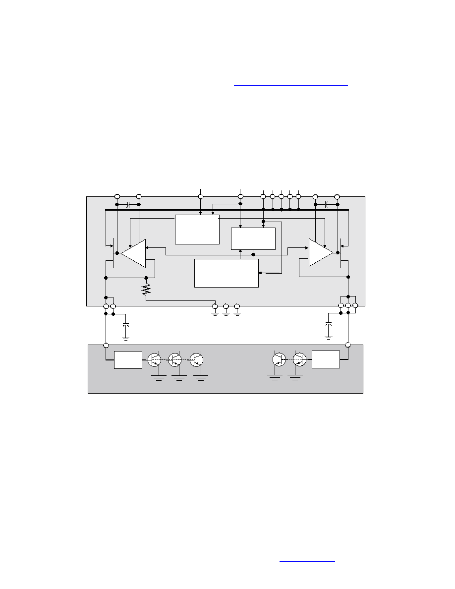
CMOS Bias Controller Characteristics
CMOS Bias Controller Characteristics
CMOS Bias Controller Characteristics
CMOS Bias Controller Characteristics
The CMOS die within the PAM performs several functions that are
important to the overall module performance. Some of these
functions must be considered for development of the power
ramping features in a 3GPP compliant transmitter power control
loop.
Please refer to 3GPP TS 05.05, Digital Cellular Communica
Please refer to 3GPP TS 05.05, Digital Cellular Communica
Please refer to 3GPP TS 05.05, Digital Cellular Communica
Please refer to 3GPP TS 05.05, Digital Cellular Communica----
tions System (Phase 2+); Radio Transmission and Reception.
tions System (Phase 2+); Radio Transmission and Reception.
tions System (Phase 2+); Radio Transmission and Reception.
tions System (Phase 2+); Radio Transmission and Reception.
All GSM specifications are now the responsibility of 3
All GSM specifications are now the responsibility of 3
All GSM specifications are now the responsibility of 3
All GSM specifications are now the responsibility of 3GPP.
GPP.
GPP.
GPP.
The standards are available at
The standards are available at
The standards are available at
The standards are available at
http://www.3GPP.org/specs/specs.htm
http://www.3GPP.org/specs/specs.htm
http://www.3GPP.org/specs/specs.htm
http://www.3GPP.org/specs/specs.htm
.
.
.
.
Power ramping considerations will be discussed later in this sec-
tion. The four main functions that will be described in this section
are Standby Mode Control, Band Select, Voltage Clamp, and
Current Buffer. The functional block diagram is shown in
Figure
7.
Dual Band GaAs Power Amplifier Die
Bandgap
Reference
Combinational
Logic
CMOS bias controller
ground
Supply
(pin 6)
C
bypass
C
bypass
RF
Isolation
RF
Isolation
Voltage Clamp
APC input
(pin 14)
Band
Select
(pin 16)
GSM900
bias out
DCS1800/
PCS1900
bias out
C
Comp
C
Comp
cpdcs
vodcs
vogsm
cpgsm
100956_008
Figure
Figure
Figure
Figure 7
7
7
7. Functional Block Diagram
. Functional Block Diagram
. Functional Block Diagram
. Functional Block Diagram
Standby Mode Control
Standby Mode Control
Standby Mode Control
Standby Mode Control
The Combinational Logic cell includes enable circuitry that
monitors the APC ramping voltage from the power amplifier con-
troller (PAC) circuit in the GSM transmitter. Typical handset de-
signs directly connect the PA V
CC
to the battery at all times, and
for some PA manufacturers this requires a control signal to set
the device in or out of standby mode. The Skyworks PAM does
not require a Transmit Enable input because it contains a standby
detection circuit that senses the V
APC
to enable or disable the PA.
This feature helps minimize battery discharge when the PA is in
standby mode. When V
APC
is below the enable threshold voltage,
the PA goes into a standby mode, which reduces battery current
(I
CC
)
to 6
µA, typical, under nominal conditions.
For voltages less than 700 mV at the APC input (pin 14), the PA
bias is held at ground. As the APC input exceeds the enable
threshold, the bias will activate. After an 8
µs delay, the amplifier
internal bias will ramp quickly to match the ramp voltage applied
to the APC input. In order for the internal bias to precisely follow
the APC ramping voltage, it is critical that a ramp pedestal is set
to the APC input at or above the enable threshold level with a
timing at least 8
µs prior to ramp-up. This will be discussed in
more detail in the following section, "Power Ramping Considera-
tions for 3GPP Compliance".
Data Sheet ∑ CX77301
PA Module for Dual-band EGSM900 DCS1800 / GPRS
12
Skyworks Solutions, Inc. Proprietary Information
SEPTEMBER 19, 2003
[781] 376-7000 ∑ FAX [781] 376-3100 ∑ SALES@SKYWORKSINC.COM ∑
WWW.SKYWORKSINC.COM
100956E
Band Select
Band Select
Band Select
Band Select
The Combinational Logic cell also includes a simple gate ar-
rangement that selects the desired operational band by activating
the appropriate current buffer. The voltage threshold level at the
Band Select input (pin 16) will determine the active path of the
bias output to the GaAs die.
Voltage Clamp
Voltage Clamp
Voltage Clamp
Voltage Clamp
The Voltage Clamp circuit will limit the maximum bias voltage
output applied to the bases of the HBT devices on the GaAs die.
This provides protection against electrical overstress (EOS) of the
active devices during high voltage and/or load mismatch condi-
tions.
Figure 8
shows the typical transfer function of the APC
input to buffer output under resistively loaded conditions. Notice
the enable function near 600 mV, and the clamp acting at 2.15 V,
corresponding to a supply voltage of 4.0 V.
0.0
0.5
1.0
1.5
2.0
2.5
0.0
0.5
1.0
1.5
2.0
2.5
3.0
APC Input (volts)
Base Bias (volts)
clamping
occurs
100956_009
Figure
Figure
Figure
Figure 8
8
8
8. Base Bias Voltage vs. APC Input, V
. Base Bias Voltage vs. APC Input, V
. Base Bias Voltage vs. APC Input, V
. Base Bias Voltage vs. APC Input, V
CC
CC
CC
CC
= 4.0 V
= 4.0 V
= 4.0 V
= 4.0 V
Due to output impedance effects, the bias of the GaAs devices
increases as the supply voltage increases. The Voltage Clamp is
designed to gradually decrease in level as the battery voltage
increases. The performance of the clamp circuit is enhanced by
the band gap reference that provides a supply-, process-, and
temperature-independent reference voltage. The transfer function
relative to V
BAT
is shown in
Figure 9
. For battery voltages below
3.4 V, the base bias voltage is limited by the common mode
range of the buffer amplifier. For battery voltages above 3.4 V,
the clamp limits the base bias.
1.7
1.8
1.9
2.0
2.1
2.2
2.3
2.4
2.5
2.6
3.00
3.25
3.50
3.75
4.00
4.25
4.50
V
cc
(Volts)
Base Bias Clamp (Volts)
clam p
100956_010
Figure
Figure
Figure
Figure 9
9
9
9. Base Bias Clamp vs. Supply Voltage
. Base Bias Clamp vs. Supply Voltage
. Base Bias Clamp vs. Supply Voltage
. Base Bias Clamp vs. Supply Voltage
Current Buffer
Current Buffer
Current Buffer
Current Buffer
The output buffer amplifier performs a vital function in the CMOS
device by transferring the APC input voltage ramp to the base of
the GaAs power devices. This allows the APC input to be a high
impedance port, sinking only 10
µA, typical, assuring no loading
effects on the PAC circuit. The buffers are designed to source the
high GaAs base currents required, while allowing a settling time
of less than 8
µs for a 1.5 V ramp.
POWER RAMPING CONSID
POWER RAMPING CONSID
POWER RAMPING CONSID
POWER RAMPING CONSIDERATIONS FOR 3GPP
ERATIONS FOR 3GPP
ERATIONS FOR 3GPP
ERATIONS FOR 3GPP
COMPLIANCE
COMPLIANCE
COMPLIANCE
COMPLIANCE
These are the primary variables in the power control loop that the
system designer must control:
∑ software control of the DSP / DAC
∑ software control of the transmitter timing signals
∑ ramp profile attributes - pedestal, number of steps, duration of
steps
∑ layout of circuit / parasitics
∑ RC time constants within the PAC circuit design
All of these variables will directly influence the ability of a GSM
transmitter power control loop to comply with 3GPP
specifications.
Although there is a specific time mask template in which the
transmitter power is allowed to ramp up, the method is very
critical. The 3GPP system specification for switching transients
results in a requirement to limit the edge rate of output power
transitions of the mobile. Switching transients are caused by the
transition from minimum output power to the desired output
power, and vice versa. The spectrum generated by this transition
is due to the ramping waveform amplitude modulation imposed
on the carrier. Sharper transitions tend to produce more spectral
"splatter" than smooth transitions. If the transmit output power is
ramped up too slowly, the radio will violate the time mask
specification. In this condition, the radio may not successfully
initiate or maintain a phone call. If the transmit output power is
ramped up too quickly, this will cause RF "splatter" at certain
frequency offsets from the carrier as dictated by the 3GPP
specification. This splatter, known as Output RF Spectrum (ORFS)
due to Switching Transients, will increase the system noise level,
which may knock out other users on the system. The main
difficulty with TDMA power control is allowing the transmitter to
ramp the output power up and down gradually so switching
transients are not compromised while meeting the time mask
template at all output power levels in all operational bands. The
transmitter has 28
µs to ramp up power from an off state to the
desired power level.
The GSM transmitter power control loop generally involves
feedback around the GaAs PA, which limits the bandwidth of
signals that can be applied to the PA bias input. Since the PA is
within the feedback loop, its own small-signal frequency
response must exhibit a bandwidth 5 to 10 times that of the
power control loop. As discussed in the previous section, the PA
bias is held at ground for inputs less than 700 mV. As the APC
input exceeds the enable threshold, the bias will activate. After

PA Module for Dual-band EGSM900 DCS1800 / GPRS
Data Sheet ∑ CX77301
Skyworks Solutions, Inc. Proprietary Information
13
100956E
[781] 376-7000 ∑ FAX [781] 376-3100 ∑ SALES@SKYWORKSINC.COM ∑
WWW.SKYWORKSINC.COM
SEPTEMBER 19, 2003
an 8
µs delay, the amplifier internal bias will quickly ramp to
match the ramp voltage applied to the VAPC input. Since the bias
must be wide band relative to the power control loop, the ramp
will exhibit a fast edge rate. If the APC input increases beyond 1
volt before the 8
µs switching delay is allowed to occur after the
bias is enabled, the PA will have significant RF output as the
internal bias approaches the applied bias. During this ramp, the
internal power control is running "open loop" and the edge rates
are defined by the frequency response of the PA bias rather than
that of the power control loop. This open loop condition will result
in switching transients that are directly correlated to the PA bias
bandwidth.
Application of an initial APC voltage, which enables the bias at
least 8
µs before the VAPC voltage is ramped, will ensure that the
internal bias of the PAM will directly follow the applied VAPC. As a
result, the power control loop will define all edge transitions
rather than the PA internal bandwidth defining the transition.
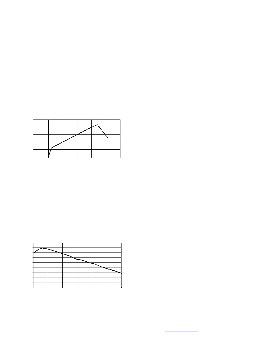
Figure 10
and
Figure 11
show the relationship of the internal bias
relative to the applied APC in two cases. One case has ramping
starting from ground; the other case has ramping starting with an
initial enable pedestal of 700 mV. It is evident that the pedestal
level is critical to ensure a predictable and well behaved power
control loop.
To enable the CMOS driver in the PAM prior to ramp-up, a PAC
output pedestal level to the APC input of the PAM (pin 14) should
be set to about 700 mV. This pedestal level should have a
duration of at least 8
µs directly prior to the start of ramp up.
Figure 12
shows typical signals and timings measured in a GSM
transmitter power control loop. This particular example is at GSM
Power Level 5, Channel 62. The oscilloscope traces are
TxVCO_enable, PAC_enable, DAC Ramp, and VAPC (pin 14).
NOTE:
When the TxVCO is enabled, the pedestal becomes set
at the APC input of the PAM, then the PAC is enabled, and finally
the DAC ramp begins.
The device specifications for enable threshold level and switching
delay are shown in
Table 3
.
0.0
0.2
0.4
0.6
0.8
1.0
1.2
1.4
1.6
0
5
10
15
20
25
30
35
Time (sec)
Bias Voltage (V)
V
APC
In (V)
Internal Bias (V)
100956_011
Figure
Figure
Figure
Figure 10
10
10
10. PAM Internal Bias Performance
. PAM Internal Bias Performance
. PAM Internal Bias Performance
. PAM Internal Bias Performance ≠
≠
≠
≠ No Pedestal Applied
No Pedestal Applied
No Pedestal Applied
No Pedestal Applied
0.0
0.2
0.4
0.6
0.8
1.0
1.2
1.4
1.6
0
5
10
15
20
25
30
35
Time (sec)
Bias Voltage (V)
V
APC
In (V)
Internal Bias (V)
100956_012
Figure
Figure
Figure
Figure 11
11
11
11. PAM Internal Bias Performance
. PAM Internal Bias Performance
. PAM Internal Bias Performance
. PAM Internal Bias Performance ≠
≠
≠
≠ Pedestal Applied
Pedestal Applied
Pedestal Applied
Pedestal Applied
PAC_enable
V
APC
DAC Ramp
V
APC
Pedestal
TxVCO_enable
100956_013
Ch1
4
3
2
1
Ch3
A
M
Ch2
Ch4
200 mV
1.00 V
BW
500 mV
Ch2
10.0 µs
1.00 V
500 mV
T
Figure
Figure
Figure
Figure 12
12
12
12. GSM Transmitter
. GSM Transmitter
. GSM Transmitter
. GSM Transmitter ≠
≠
≠
≠ Typical Ramp
Typical Ramp
Typical Ramp
Typical Ramp----up Signals
up Signals
up Signals
up Signals

ORDERING INFORMATION
ORDERING INFORMATION
ORDERING INFORMATION
ORDERING INFORMATION
Model Number
Model Number
Model Number
Model Number
Manufacturing
Manufacturing
Manufacturing
Manufacturing
Part Number
Part Number
Part Number
Part Number
Product Revision
Product Revision
Product Revision
Product Revision
Package
Package
Package
Package
Operating Temperature
Operating Temperature
Operating Temperature
Operating Temperature
CX77301
CX77301
≠13
9.1 x 11.6 x 1.5 mm
≠20 ◊C to +100 ◊C
REVISION HISTORY
REVISION HISTORY
REVISION HISTORY
REVISION HISTORY
Revision
Revision
Revision
Revision
Level
Level
Level
Level
Date
Date
Date
Date
Description
Description
Description
Description
A
June 2000
Initial Release
B
January 2001
Add: Tables 3,4
Revise: Figure 4.
C
March 2001
Add: ESD data, revised format to add chapter headings
D
January 2, 2002
Add: Technical Information Section
Revise: Functional Block Diagram; ESD data (+/≠ thresholds),
Figure 10.
E
September 19, 2003
New format
Add: Figure 4
Revise: Figures 3, 5, 6
REFERENCES
REFERENCES
REFERENCES
REFERENCES
Application Note: PCB Design and SMT Assembly/Rework, Document Number 101752
Application Note: Tape and Reel, Document Number 101568
JEDEC Standard J≠STD≠020B
© 2001≠2003, Skyworks Solutions, Inc. All Rights Reserved.
Information in this document is provided in connection with Skyworks Solutions, Inc. ("Skyworks") products. These materials are provided by Skyworks as a service to its
customers and may be used for informational purposes only. Skyworks assumes no responsibility for errors or omissions in these materials. Skyworks may make changes
to its products, specifications and product descriptions at any time, without notice. Skyworks makes no commitment to update the information and shall have no
responsibility whatsoever for conflicts, incompatibilities, or other difficulties arising from future changes to its products and product descriptions.
No license, express or implied, by estoppel or otherwise, to any intellectual property rights is granted by this document. Except as may be provided in Skyworks' Terms
and Conditions of Sale for such products, Skyworks assumes no liability whatsoever.
THESE MATERIALS ARE PROVIDED "AS IS" WITHOUT WARRANTY OF ANY KIND, EITHER EXPRESS OR IMPLIED, RELATING TO SALE AND/OR USE OF SKYWORKSTM
PRODUCTS INCLUDING WARRANTIES RELATING TO FITNESS FOR A PARTICULAR PURPOSE, MERCHANTABILITY, PERFORMANCE, QUALITY OR NON-INFRINGEMENT OF ANY
PATENT, COPYRIGHT OR OTHER INTELLECTUAL PROPERTY RIGHT. SKYWORKS FURTHER DOES NOT WARRANT THE ACCURACY OR COMPLETENESS OF THE
INFORMATION, TEXT, GRAPHICS OR OTHER ITEMS CONTAINED WITHIN THESE MATERIALS. SKYWORKS SHALL NOT BE LIABLE FOR ANY SPECIAL, INDIRECT, INCIDENTAL,
OR CONSEQUENTIAL DAMAGES, INCLUDING WITHOUT LIMITATION, LOST REVENUES OR LOST PROFITS THAT MAY RESULT FROM THE USE OF THESE MATERIALS.
SkyworksTM products are not intended for use in medical, lifesaving or life-sustaining applications. Skyworks' customers using or selling SkyworksTM products for use in
such applications do so at their own risk and agree to fully indemnify Skyworks for any damages resulting from such improper use or sale.
The following are trademarks of Skyworks Solutions, Inc.: SkyworksTM, the Skyworks symbol, and "Breakthrough Simplicity"TM. Product names or services listed in this
publication are for identification purposes only, and may be trademarks of third parties. Third-party brands and names are the property of their respective owners.
Additional information, posted at www.skyworksinc.com, is incorporated by reference.
General Information
Skyworks Solutions, Inc.
20 Sylvan Rd.
Woburn, MA 01801
www.skyworksinc.com
www.skyworksinc.com
www.skyworksinc.com
www.skyworksinc.com