
Skyworks Solutions, Inc. ∑ Phone [781] 376-3000 ∑ Fax [781] 376-3100 ∑ sales@skyworksinc.com ∑ www.skyworksinc.com
200046 Rev. C ∑ Skyworks Proprietary Information ∑ Products and Product Information are Subject to Change Without Notice. ∑ February 21, 2005
1
SMP1345 Series: Very Low Capacitance
Plastic Packaged Silicon PIN Diodes
DATA SHEET
Characteristic
Value
Reverse voltage (V
R
)
50 V
Power dissipation @ 25 ∞C lead
250 mW
temperature (P
D
)
Storage temperature (T
ST
)
-65 ∞C to +150 ∞C
Operating temperature (T
OP
)
-65 ∞C to +150 ∞C
ESD human body model
Class 1B
Absolute Maximum Ratings
Features
Designed for high isolation LNB, WLAN and wireless
switch applications
Very low insertion loss (0.4 dB)
0.15 pF capacitance
Available lead (Pb)-free MSL-1 @ 250 ∞C per JEDEC J-STD-020
Available in tape and reel packaging
Description
The SMP1345 series of plastic packaged, surface mountable PIN
diodes is designed for high volume LNB, WLAN and switch applica-
tions from 10 MHz to 6 GHz. The short carrier lifetime of typically
100 ns, combined with its thin I region width of nominally, 10
µm,
results in a fast speed RF switching PIN diode. The RF performance
of the SMP1345 series is assured by virtue of its very low capaci-
tance (0.15 pF) and low resistance (1.5
at 10 mA).
The SMP1345-518 has been specifically designed for WLAN
802.11 a, b, and g applications. It is ideally used for diversity
switch applications.
Skyworks offers lead (Pb)-free "environmentally
friendly" packaging that is RoHS compliant
(European Parliament for the Restriction of
Hazardous Substances).
NEW
Performance is guaranteed only under the conditions listed in the specifications table and is
not guaranteed under the full range(s) described by the Absolute Maximum specifications.
Exceeding any of the absolute maximum/minimum specifications may result in permanent
damage to the device and will void the warranty.
CAUTION: Although this device is designed to be as robust as
possible, Electrostatic Discharge (ESD) can damage
this device. This device must be protected at all times
from ESD. Static charges may easily produce poten-
tials of several kilovolts on the human body or
equipment, which can discharge without detection.
Industry-standard ESD precautions must be employed
at all times.
Skyworks Solutions, Inc. ∑ Phone [781] 376-3000 ∑ Fax [781] 376-3100 ∑ sales@skyworksinc.com ∑ www.skyworksinc.com
February 21, 2005 ∑ Skyworks Proprietary Information ∑ Products and Product Information are Subject to Change Without Notice. ∑ 200046 Rev. C
DATA SHEET ∑ SMP1345 SERIES
2
Total Capacitance vs. Reverse Voltage
Measured in an SC-79 Package
Reverse Voltage (V)
Capacitance (pF)
0
5
10
15
25
20
30
0.05
0.10
0.15
0.20
Series Resistance vs. Current @ 100 MHz
0.01
0.1
1
10
100
Forward Current (mA)
Series Resistance (
)
0.01
0.1
1
10
100
Typical Performance Data
Parameter
Condition
Typ.
Max.
Unit
Reverse current (I
R
)
V
R
= 50 V
10
µA
Capacitance (C
T
)
F = 1 MHz, V = 1 V
0.19
pF
Capacitance (C
T
)
F = 1 MHz, V = 5 V
0.18
0.20
pF
Resistance (R
S
)
F = 100 MHz, I = 1 mA
3.50
Resistance (R
S
)
F = 100 MHz, I = 10 mA
1.50
2.00
Forward voltage (V
F
)
I
F
= 10 mA
0.89
V
Carrier lifetime (TI)
I
F
= 10 mA
100
ns
I region width
10
µm
Electrical Specifications at 25 ∞C
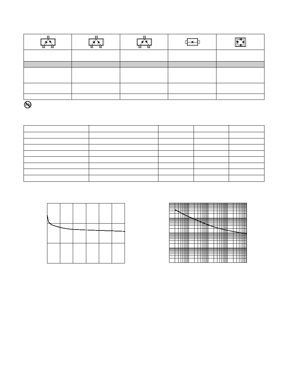
Common Common
Series
Anode
Cathode
Pair
Single
Ring
SOT-23
SOT-23
SOT-23
SC-79
LGA
SMP1345-003
SMP1345-004
SMP1345-005
SMP1345-079
SMP1345-518
Marking: PU9
Marking: PU3
Marking: PU2
Lead (Pb)-Free
Marking: 0
SMP1345-003LF
SMP1345-004LF
SMP1345-005LF
SMP1345-079LF
Marking: RU9
Marking: RU3
Marking: RU2
L
S
= 1.5 nH
L
S
= 1.5 nH
L
S
= 1.5 nH
L
S
= 0.7 nH
L
S
= 0.6 nH
LF denotes lead (Pb)-free packaging option as an alternative to our standard
tin/lead (Sn/Pb) packaging.

DATA SHEET ∑ SMP1345 SERIES
Skyworks Solutions, Inc. ∑ Phone [781] 376-3000 ∑ Fax [781] 376-3100 ∑ sales@skyworksinc.com ∑ www.skyworksinc.com
200046 Rev. C ∑ Skyworks Proprietary Information ∑ Products and Product Information are Subject to Change Without Notice. ∑ February 21, 2005
3
R
4
L
4
C
8
CTR2
V
DC
= 3.3 V
RF1
C
4
C
7
L
3
R
3
V
DC
= 3.3 V
CTR1
RF
4
R
1
≠R
4
0402 200
L
1
≠L
4
0603 18 nH
C
1
≠C
8
0402 10 pF
C
3
C
6
V
DC
= 3.3 V
CTR2
R
2
L
2
C
2
RF2
C
5
CTR1
R
1
L
1
V
DC
= 3.3 V
C
1
U
1
RF3
SMP1345-518
WLAN Application Circuit for DPDT Diversity
Switch Using SMP1345-518
SMP1345-518
EVAL BOARD
REV 1
SK40253
RF4
C
3
RF2
C
2
RF3
C
1
R
2
C
6
L
2
R
4
C
8
L
4
C
7
R
3
RF1
C
4
L
3
CTR2
CTR1
C
5
R
1
L
1
2.000
1.500
0.014
Evaluation Board
Bridge Switch Schematic
CTR1
CTR2
Low Loss Paths
3.3 V
0 V
RF1≠RF4
RF2≠RF3
0 V
3.3 V
RF1≠RF3
RF2≠RF4
Truth Table

Skyworks Solutions, Inc. ∑ Phone [781] 376-3000 ∑ Fax [781] 376-3100 ∑ sales@skyworksinc.com ∑ www.skyworksinc.com
February 21, 2005 ∑ Skyworks Proprietary Information ∑ Products and Product Information are Subject to Change Without Notice. ∑ 200046 Rev. C
DATA SHEET ∑ SMP1345 SERIES
4
Insertion Loss vs. Frequency
Frequency (GHz)
Insertion Loss
1.0
2.0
3.0
4.0
-2.4
-1.0
-1.2
-1.4
-1.6
-1.8
-2.0
-2.2
-0.4
-0.6
-0.8
-0.2
Isolation vs. Frequency
Frequency (GHz)
Isolation
1.0
2.0
3.0
4.0
-32
-18
-20
-22
-24
-26
-28
-30
Return Loss vs. Frequency
Frequency (GHz)
Return Loss
1.0
2.0
3.0
4.0
-20
-21
-22
-23
-24
-25
-13
-14
-15
-16
-17
-18
-19
Typical Performance Data For SMP1345-518

DATA SHEET ∑ SMP1345 SERIES
Skyworks Solutions, Inc. ∑ Phone [781] 376-3000 ∑ Fax [781] 376-3100 ∑ sales@skyworksinc.com ∑ www.skyworksinc.com
200046 Rev. C ∑ Skyworks Proprietary Information ∑ Products and Product Information are Subject to Change Without Notice. ∑ February 21, 2005
5
SOT-23
3
2
1
0.035 (0.89 mm) Min.
0.044 (1.12 mm) Max.
0.0005 (0.01 mm) Min.
0.004 (0.10 mm) Max.
0.012 (0.30 mm) Min.
0.020 (0.50 mm) Max.
0.003 (0.080 mm) Min.
0.008 (0.20 mm) Max.
8∞ Max.
0.022 (0.55 mm) Ref.
0.110 (2.80 mm) Min.
0.120 (3.04 mm) Max.
0.083 (2.10 mm) Min.
0.104 (2.64 mm) Max.
0.037 (0.95 mm) Ref.
0.047 (1.20 mm) Min.
0.055 (1.40 mm) Max.
0.076 (1.92 mm) Ref.
0.020 (0.51 mm) Ref.
SC-79
0.060 (1.50 mm) Min.
0.067 (1.70 mm) Max.
0.010
(0.25 mm) Min.
0.014
(0.35 mm) Max.
0.043 (1.10 mm) Min.
0.051 (1.30 mm) Max.
0.020
(0.50 mm) Min.
0.028
(0.70 mm) Max.
0.003
(0.07 mm) Min.
0.008
(0.20 mm) Max.
10∞ Max.
10∞ Max.
0.028
(0.70 mm) Min.
0.035
(0.90 mm) Max.
0.006 (0.15 mm) Min.
Cathode
Indicator
1
2
LGA
Pin 2
Pin 1
Pin 3
Pin 1
Pin 3
Pin 4
Pin 4
(1.03)
(0.73)
(0.30)
(0.00)
Pin 2
0.058 (1.47 mm)
0.054 (1.39 mm)
0.028 (0.70 mm)
0.023 (0.58 mm)
Side View
Top View
0.048 (1.23 mm)
0.044 (1.13 mm)
(0.138 x 45)
(1.27)
(0.87)
(0.40)
(0.00)
Bottom View
(0.076) All Around
Recommended Solder Reflow Profiles
Refer to the "Recommended Solder Reflow Profile"
Application Note.