
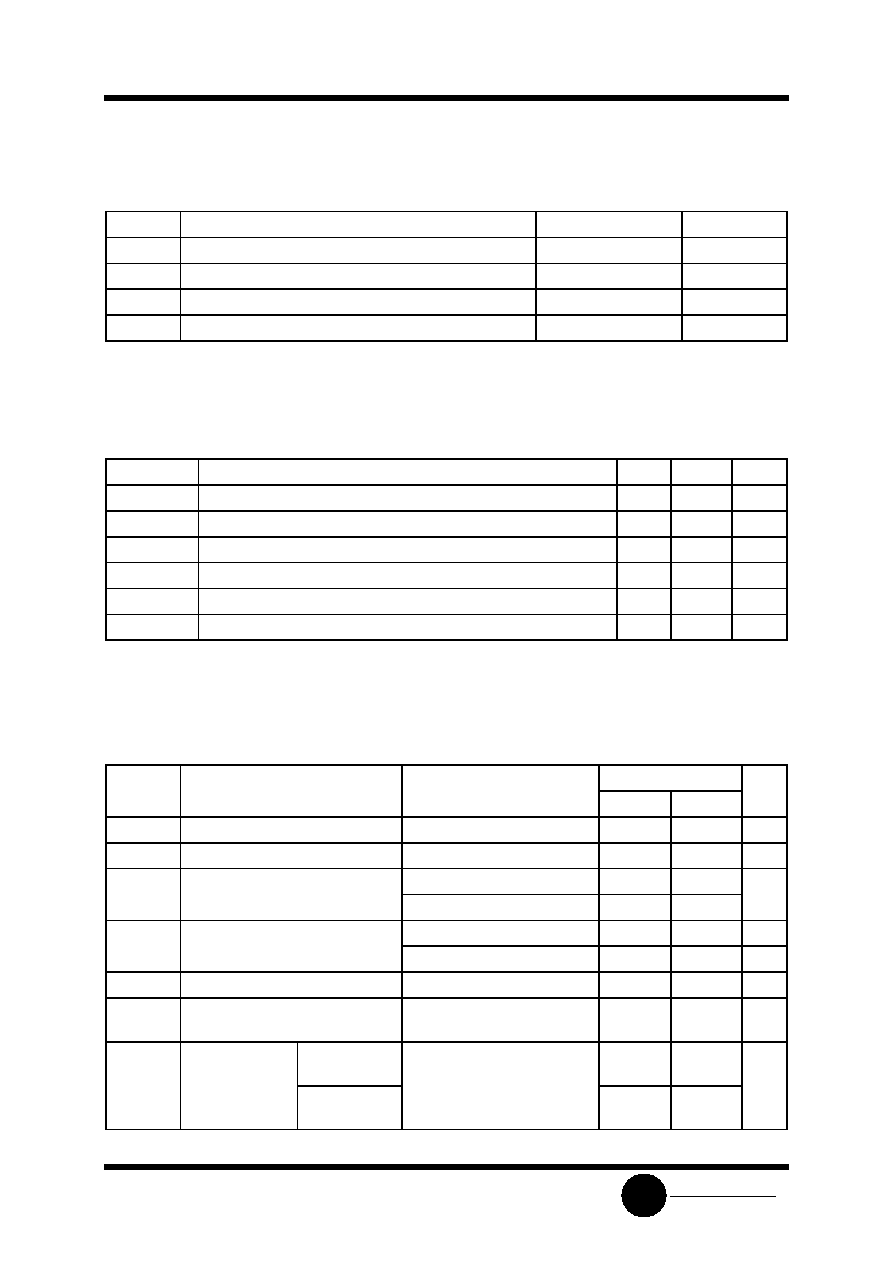
SL74LS86
System Logic
Semiconductor
SLS
Quad 2-Input Exclusive OR
Gate
This device contains four independent 2-input Exclusive-OR gates.
It performs the Boolean functions Y=A
B=AB+AB in positive logic.
ORDERING INFORMATION
SL74LS86N Plastic
SL74LS86D SOIC
T
A
= 0
∞
to 70
∞
C for all
packages
LOGIC DIAGRAM
PIN 14 =V
CC
PIN 7 = GND
PIN ASSIGNMENT
FUNCTION TABLE
Inputs
Output
A
B
Y
L
L
L
L
H
H
H
L
H
H
H
L
SL74LS86
System Logic
Semiconductor
SLS
MAXIMUM RATINGS
*
Symbol
Parameter
Value
Unit
V
CC
Supply Voltage
7.0
V
V
IN
Input Voltage
7.0
V
V
OUT
Output Voltage
5.5
V
Tstg
Storage Temperature Range
-65 to +150
∞
C
*
Maximum Ratings are those values beyond which damage to the device may occur.
Functional operation should be restricted to the Recommended Operating Conditions.
RECOMMENDED OPERATING CONDITIONS
Symbol
Parameter
Min
Max
Unit
V
CC
Supply Voltage
4.75
5.25
V
V
IH
High Level Input Voltage
2.0
V
V
IL
Low Level Input Voltage
0.8
V
I
OH
High Level Output Current
-0.4
mA
I
OL
Low Level Output Current
8.0
mA
T
A
Ambient Temperature Range
0
+70
∞
C
DC ELECTRICAL CHARACTERISTICS
over full operating conditions
Guaranteed Limit
Symbol
Parameter
Test Conditions
Min
Max
Unit
V
IK
Input Clamp Voltage
V
CC
= min, I
IN
= -18 mA
-1.5
V
V
OH
High Level Output Voltage
V
CC
= min, I
OH
= -0.4 mA
2.7
V
V
OL
Low Level Output Voltage
V
CC
= min, I
OL
= 4 mA
0.4
V
V
CC
= min, I
OL
= 8 mA
0.5
I
IH
High Level Input Current
V
CC
= max, V
IN
= 2.7 V
40
µ
A
V
CC
= max, V
IN
= 7.0 V
0.2
mA
I
IL
Low Level Input Current
V
CC
= max, V
IN
= 0.4 V
-0.8
mA
I
O
Output Short Circuit Current
V
CC
= max, V
O
= 0 V
(Note 1)
-20
-100
mA
I
CC
Supply Current
Total with
outputs high
V
CC
= max
10
mA
Total with
outputs low
15
Note 1: Not more than one output should be shorted at a time, and duration should not exceed one second.
SL74LS86
System Logic
Semiconductor
SLS
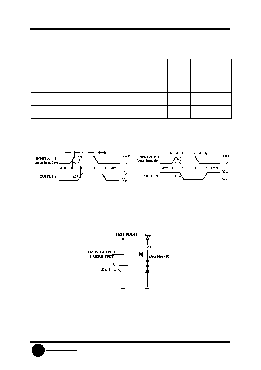
AC ELECTRICAL CHARACTERISTICS
(T
A
=25
∞
C, V
CC
= 5.0 V, C
L
= 15 pF, R
L
= 2 k
, t
r
=15
ns, t
f
= 6.0 ns)
Symbol
Parameter
Min
Max
Unit
t
PLH
Propagation Delay, Input A or B to Output Y
(Other input low)
23
ns
t
PHL
Propagation Delay, Input A or B to Output Y
(Other input low)
17
ns
t
PLH
Propagation Delay, Input A or B to Output Y
(Other input high)
30
ns
t
PHL
Propagation Delay, Input A or B to Output Y
(Other input high)
22
ns
Figure 1. Switching Waveforms
Figure 2. Switching Waveforms
NOTES A. C
L
includes probe and jig capacitance.
B. All diodes are 1N916 or 1N3064.
Figure 3. Test Circuit