 | –≠–ª–µ–∫—Ç—Ä–æ–Ω–Ω—ã–π –∫–æ–º–ø–æ–Ω–µ–Ω—Ç: SL503BN | –°–∫–∞—á–∞—Ç—å:  PDF PDF  ZIP ZIP |
SL4503B
System Logic
Semiconductor
SLS
Hex Buffer
High-Voltage Silicon-Gate CMOS
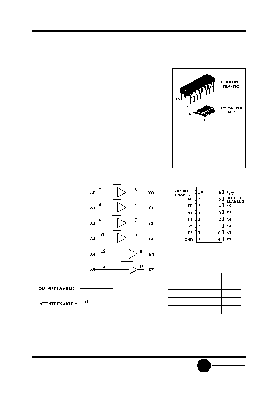
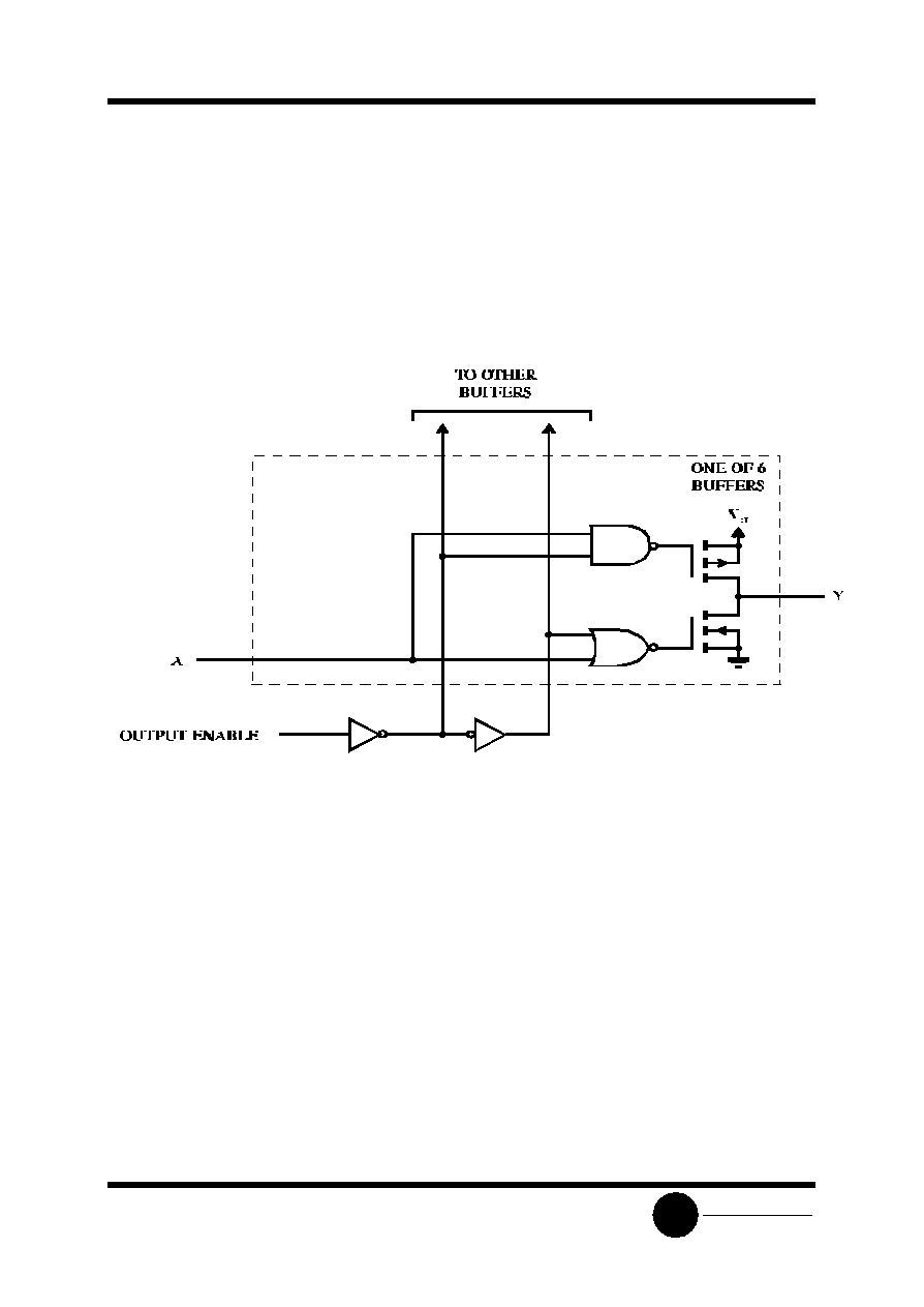
The SL4503B is a hex noninverting buffer with 3-state outputs
having high sink- and source-current capability. Two output ENABLE
controls are provided, one of which controls four buffers and the other
controls the remaining two buffers.
∑
Operating Voltage Range: 3.0 to 18 V
∑
Maximum input current of 1
µ
A at 18 V over full package-
temperature range; 100 nA at 18 V and 25
∞
C
∑
Nois e margin (over full package temperature range):
1.0 V min @ 5.0 V supply
2.0 V min @ 10.0 V supply
2.5 V min @ 15.0 V supply
ORDERING INFORMATION
SL503BN Plastic
SL4503BD SOIC
T
A
= -55
∞
to 125
∞
C for all packages
LOGIC DIAGRAM
PIN 16=V
CC
PIN 8= GND
PIN ASSIGNMENT
FUNCTION TABLE
Inputs
Output
Enable 1,Enable 2
A
Y
L
L
L
L
H
H
H
X
Z
Z = high impedance
X = don't care

SL4503B
System Logic
Semiconductor
SLS
MAXIMUM RATINGS
*
Symbol
Parameter
Value
Unit
V
CC
DC Supply Voltage (Referenced to GND)
-0.5 to +20
V
V
IN
DC Input Voltage (Referenced to GND)
-0.5 to V
CC
+0.5
V
V
OUT
DC Output Voltage (Referenced to GND)
-0.5 to V
CC
+0.5
V
I
IN
DC Input Current, per Pin
±
10
mA
P
D
Power Dissipation in Still Air, Plastic DIP+
SOIC Package+
750
500
mW
P
D
Power Dissipation per Output Transistor
100
mW
Tstg
Storage Temperature
-65 to +150
∞
C
T
L
Lead Temperature, 1 mm from Case for 10 Seconds
(Plastic DIP or SOIC Package)
260
∞
C
*
Maximum Ratings are those values beyond which damage to the device may occur.
Functional operation should be restricted to the Recommended Operating Conditions.
+Derating - Plastic DIP: - 10 mW/
∞
C from 65
∞
to 125
∞
C
SOIC Package: : - 7 mW/
∞
C from 65
∞
to 125
∞
C
RECOMMENDED OPERATING CONDITIONS
Symbol
Parameter
Min
Max
Unit
V
CC
DC Supply Voltage (Referenced to GND)
3.0
18
V
V
IN
, V
OUT
DC Input Voltage, Output Voltage (Referenced to GND)
0
V
CC
V
T
A
Operating Temperature, All Package Types
-55
+125
∞
C
This device contains protection circuitry to guard against damage due to high static voltages or electric
fields. However, precautions must be taken to avoid applications of any voltage higher than maximum rated
voltages to this high-impedance circuit. For proper operation, V
IN
and V
OUT
should be constrained to the range
GND
(V
IN
or V
OUT
)
V
CC
.
Unused inputs must always be tied to an appropriate logic voltage level (e.g., either GND or V
CC
).
Unused outputs must be left open.

SL4503B
System Logic
Semiconductor
SLS
DC ELECTRICAL CHARACTERISTICS
(Voltages Referenced to GND)
V
CC
Guaranteed Limit
Symbol
Parameter
Test Conditions
V
-55
∞
C
25
∞
C
125
∞
C
Unit
V
IH
Minimum High-Level
Input Voltage
V
OUT
= V
CC
- 0.5V
V
OUT
= V
CC
- 1.0 V
V
OUT
= V
CC
- 1.5V
5.0
10
15
3.5
7
11
3.5
7
11
3.5
7
11
V
V
IL
Maximum Low -Level
Input Voltage
V
OUT
=0.5 V
V
OUT
=1 V
V
OUT
=1.5
5.0
10
15
1.5
3
4
1.5
3
4
1.5
3
4
V
V
OH
Minimum High-Level
Output Voltage
V
IN
= V
CC
5.0
10
15
4.95
9.95
14.95
4.95
9.95
14.95
4.95
9.95
14.95
V
V
OL
Maximum Low-Level
Output Voltage
V
IN
=GND
5.0
10
15
0.05
0.05
0.05
0.05
0.05
0.05
0.05
0.05
0.05
V
I
IN
Maximum Input
Leakage Current
V
IN
= GND or V
CC
18
±
0.1
±
0.1
±
1.0
µ
A
I
CC
Maximum Quiescent
Supply Current
(per Package)
V
IN
= GND or V
CC
5.0
10
15
20
1
2
4
20
1
2
4
20
30
60
120
600
µ
A
I
OL
Minimum Output Low
(Sink) Current
V
IN
= GND or V
CC
U
OL
=0.4 V
U
OL
=0.5 V
U
OL
=1.5 V
5.0
10
15
2.6
6.5
19.2
2.1
5.5
16.1
1.3
3.8
11.2
mA
I
OH
Minimum Output High
(Source) Current
V
IN
= GND or V
CC
U
OH
=2.5 V
U
OH
=4.6 V
U
OH
=9.5 V
U
OH
=13.5 V
5.0
5.0
10
15
-1.2
-5.8
-3.1
-8.2
-1.02
-4.8
-2.6
-6.8
-0.7
-3
--1.8
-4.8
mA
I
OZ
Maximum Tree-State
Leakage Current
Output in High-Impedance
State
V
IN
= GND or V
CC
V
OUT
= GND or V
CC
18
±
0.4
±
0.4
±
12
µ
A
SL4503B
System Logic
Semiconductor
SLS
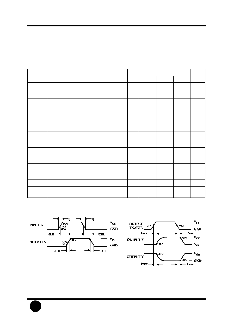
AC ELECTRICAL CHARACTERISTICS
(C
L
=50pF, R
L
=200k
unless otherwise specified, Input
t
r
=t
f
=20 ns)
V
CC
Guaranteed Limit
Symbol
Parameter
V
-55
∞
C
25
∞
C
125
∞
C
Unit
t
PLH
Maximum Propagation Delay, Input A to Output
Y (Figure 1)
5.0
10
15
150
70
50
150
70
50
300
140
100
ns
t
PHL
Maximum Propagation Delay, Input A to Output
Y (Figure 1)
5.0
10
15
110
50
35
110
50
35
220
100
70
ns
t
PHZ
, t
PZH
Maximum Propagation Delay, Output Enable to
Output Y (Figure 2)
R
L
= 1 k
5.0
10
15
140
60
50
140
60
50
280
120
100
ns
t
PZL
, t
PLZ
Maximum Propagation Delay, Output Enable to
Output Y (Figure 2)
R
L
= 1 k
5.0
10
15
180
80
70
180
80
70
360
160
140
ns
t
TLH
Maximum Output Transition Time, Any Output
(Figure 1)
5.0
10
15
90
45
35
90
45
35
180
90
70
ns
t
THL
Maximum Output Transition Time, Any Output
(Figure 1)
5.0
10
15
70
40
25
70
40
25
140
80
50
ns
C
IN
Maximum Input Capacitance
-
7.5
pF
C
OUT
Maximum Tree-State Output Capacitance
(Output in High-Impedance State)
-
15
pF
Figure 1. Switching Waveforms
Figure 2. Switching Waveforms
SL4503B
System Logic
Semiconductor
SLS
EXPANDED LOGIC DIAGRAM
(1/6 of the Device)