
SL74HC151
System Logic
Semiconductor
SLS
8-Input Data Selector/Multiplexer
High-Performance Silicon-Gate CMOS
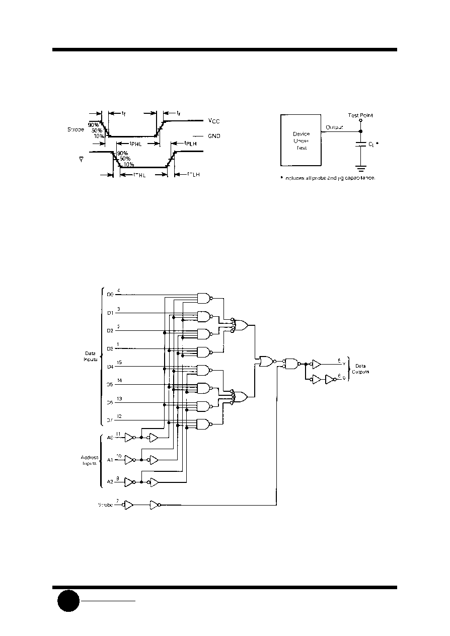
The SL74HC151 is identical in pinout to the LS/ALS151. The device
inputs are compatible with standard CMOS outputs; with pullup
resistors, they are compatible with LS/ALSTTL outputs.
The device selects one of the eight binary Data Inputs, as
determined by the Address Inputs. The Strobe pin must be at a low
level for the selected data to appear at the outputs. If Strobe is high,
the Y output is forced to a low level and the Y output is forced to a
high level.
∑
Outputs Directly Interface to CMOS, NMOS, and TTL
∑
Operating Voltage Range: 2.0 to 6.0 V
∑
Low Input Current: 1.0
µ
A
∑
High Noise Immunity Characteristic of CMOS Devices
ORDERING INFORMATION
SL74HC151N Plastic
SL74HC151D SOIC
T
A
= -55
∞
to 125
∞
C for all packages
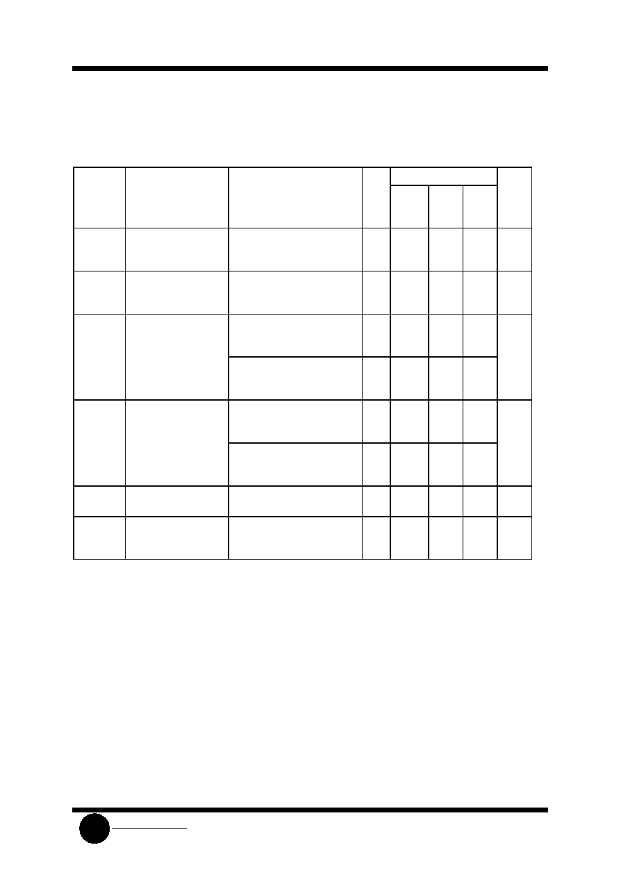
FUNCTION TABLE
Inputs
Outputs
A2 A1 A0
Strobe
Y
Y
X
X
X
H
L
H
L
L
L
L
D0
D0
L
L
H
L
D1
D1
L
H
L
L
D2
D2
L
H
H
L
D3
D3
H
L
L
L
D4
D4
H
L
H
L
D5
D5
H
H
L
L
D6
D6
H
H
H
L
D7
D7
D0,D1...D7=the level of the respective D
input
X = don't care
LOGIC DIAGRAM
PIN 16 =V
CC
PIN 8 = GND
PIN ASSIGNMENT

SL74HC151
System Logic
Semiconductor
SLS
MAXIMUM RATINGS
*
Symbol
Parameter
Value
Unit
V
CC
DC Supply Voltage (Referenced to GND)
-0.5 to +7.0
V
V
IN
DC Input Voltage (Referenced to GND)
-1.5 to V
CC
+1.5
V
V
OUT
DC Output Voltage (Referenced to GND)
-0.5 to V
CC
+0.5
V
I
IN
DC Input Current, per Pin
±
20
mA
I
OUT
DC Output Current, per Pin
±
25
mA
I
CC
DC Supply Current, V
CC
and GND Pins
±
50
mA
P
D
Power Dissipation in Still Air, Plastic DIP+
SOIC Package+
750
500
mW
Tstg
Storage Temperature
-65 to +150
∞
C
T
L
Lead Temperature, 1 mm from Case for 10 Seconds
(Plastic DIP or SOIC Package)
260
∞
C
*
Maximum Ratings are those values beyond which damage to the device may occur.
Functional operation should be restricted to the Recommended Operating Conditions.
+Derating - Plastic DIP: - 10 mW/
∞
C from 65
∞
to 125
∞
C
SOIC Package: : - 7 mW/
∞
C from 65
∞
to 125
∞
C
RECOMMENDED OPERATING CONDITIONS
Symbol
Parameter
Min
Max
Unit
V
CC
DC Supply Voltage (Referenced to GND)
2.0
6.0
V
V
IN
, V
OUT
DC Input Voltage, Output Voltage (Referenced to GND)
0
V
CC
V
T
A
Operating Temperature, All Package Types
-55
+125
∞
C
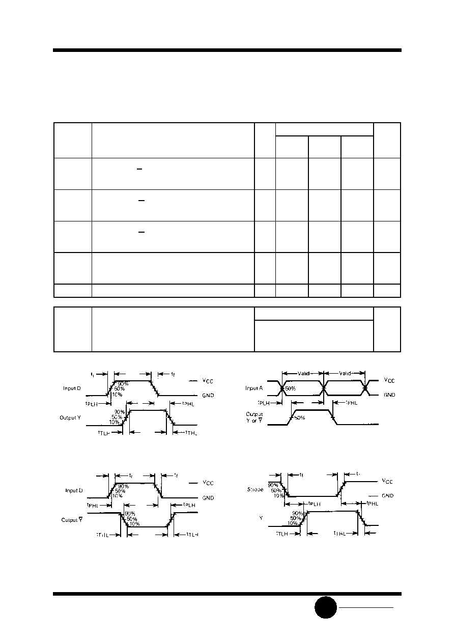
t
r
, t
f
Input Rise and Fall Time (Figure 1)
V
CC
=2.0 V
V
CC
=4.5 V
V
CC
=6.0 V
0
0
0
1000
500
400
ns
This device contains protection circuitry to guard against damage due to high static voltages or electric
fields. However, precautions must be taken to avoid applications of any voltage higher than maximum rated
voltages to this high-impedance circuit. For proper operation, V
IN
and V
OUT
should be constrained to the range
GND
(V
IN
or V
OUT
)
V
CC
.
Unused inputs must always be tied to an appropriate logic voltage level (e.g., either GND or V
CC
).
Unused outputs must be left open.
SL74HC151
System Logic
Semiconductor
SLS
DC ELECTRICAL CHARACTERISTICS
(Voltages Referenced to GND)
V
CC
Guaranteed Limit
Symbol
Parameter
Test Conditions
V
25
∞
C
to
-55
∞
C
85
∞
C
125
∞
C
Unit
V
IH
Minimum High-Level
Input Voltage
V
OUT
=0.1 V or V
CC
-0.1 V
I
OUT
20
µ
A
2.0
4.5
6.0
1.5
3.15
4.2
1.5
3.15
4.2
1.5
3.15
4.2
V
V
IL
Maximum Low -Level
Input Voltage
V
OUT
=0.1 V or V
CC
-0.1 V
I
OUT
20
µ
A
2.0
4.5
6.0
0.3
0.9
1.2
0.3
0.9
1.2
0.3
0.9
1.2
V
V
OH
Minimum High-Level
Output Voltage
V
IN
=V
IH
or V
IL
I
OUT
20
µ
A
2.0
4.5
6.0
1.9
4.4
5.9
1.9
4.4
5.9
1.9
4.4
5.9
V
V
IN
=V
IH
or V
IL
I
OUT
4.0 mA
I
OUT
5.2 mA
4.5
6.0
3.98
5.48
3.84
5.34
3.7
5.2
V
OL
Maximum Low-Level
Output Voltage
V
IN
=V
IH
or V
IL
I
OUT
20
µ
A
2.0
4.5
6.0
0.1
0.1
0.1
0.1
0.1
0.1
0.1
0.1
0.1
V
V
IN
=V
IH
or V
IL
I
OUT
4.0 mA
I
OUT
5.2 mA
4.5
6.0
0.26
0.26
0.33
0.33
0.4
0.4
I
IN
Maximum Input
Leakage Current
V
IN
=V
CC
or GND
6.0
±
0.1
±
1.0
±
1.0
µ
A
I
CC
Maximum Quiescent
Supply Current
(per Package)
V
IN
=V
CC
or GND
I
OUT
=0
µ
A
6.0
8.0
80
160
µ
A
SL74HC151
System Logic
Semiconductor
SLS
AC ELECTRICAL CHARACTERISTICS
(C
L
=50pF,Input t
r
=t
f
=6.0 ns)
V
CC
Guaranteed Limit
Symbol
Parameter
V
25
∞
C to
-55
∞
C
85
∞
C
125
∞
C
Unit
t
PLH
, t
PHL
Maximum Propagation Delay, Input D to
Output Y or Y (Figures 1,3 and 6)
2.0
4.5
6.0
185
37
31
230
46
39
280
56
48
ns
t
PLH
, t
PHL
Maximum Propagation Delay , Input A to
Output Y or Y (Figures 2 and 6)
2.0
4.5
6.0
205
41
35
255
51
43
310
62
53
ns
t
PLH
, t
PHL
Maximum Propagation Delay , Strobe to
Output Y or Y (Figures 4,5 and 6)
2.0
4.5
6.0
125
25
21
155
31
26
190
38
32
ns
t
TLH
, t
THL
Maximum Output Transition Time, Any Output
(Figures 1 and 6)
2.0
4.5
6.0
75
15
13
95
19
16
110
22
19
ns
C
IN
Maximum Input Capacitance
-
10
10
10
pF
Power Dissipation Capacitance (Per Package)
Typical @25
∞
C,V
CC
=5.0 V
C
PD
Used to determine the no-load dynamic power
consumption:
P
D
=C
PD
V
CC
2
f+I
CC
V
CC
36
pF
Figure 1. Switching Waveforms
Figure 2. Switching Waveforms
Figure 3. Switching Waveforms
Figure 4. Switching Waveforms
SL74HC151
System Logic
Semiconductor
SLS
Figure 5. Switching waveforms
Figure 6.Test Circuit
EXPANDED LOGIC DIAGRAM