 | –≠–ª–µ–∫—Ç—Ä–æ–Ω–Ω—ã–π –∫–æ–º–ø–æ–Ω–µ–Ω—Ç: SL74HCT74 | –°–∫–∞—á–∞—Ç—å:  PDF PDF  ZIP ZIP |
SL74HCT74
System Logic
Semiconductor
SLS
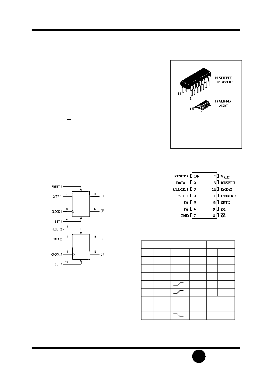
Dual D Flip-Flop with Set and Reset
High-Performance Silicon-Gate CMOS
The SL74HCT74 is identical in pinout to the LS/ALS74. This device
may be used as a level converter for interfacing TTL or NMOS outputs
to High Speed CMOS inputs.
This device consists of two D flip-flops with individual Set, Reset,
and Clock inputs. Information at a D-input is transferred to the
corresponding Q output on the next positive going edge of the clock
input. Both Q and Q outputs are available from each flip-flop. The Set
and Reset inputs are asynchronous.
∑
TTL/NMOS Compatible Input Levels
∑
Outputs Directly Interface to CMOS, NMOS, and TTL
∑
Operating Voltage Range: 4.5 to 5.5 V
∑
Low Input Current: 1.0
µ
A
ORDERING INFORMATION
SL74HCT74N Plastic
SL74HCT74D SOIC
T
A
= -55
∞
to 125
∞
C for all packages
LOGIC DIAGRAM
PIN 14 =V
CC
PIN 7 = GND
PIN ASSIGNMENT
FUNCTION TABLE
Inputs
Outputs
Set
Reset
Clock
Data
Q
Q
L
H
X
X
H
L
H
L
X
X
L
H
L
L
X
X
H
*
H
*
H
H
H
H
L
H
H
L
L
H
H
H
L
X
No Change
H
H
H
X
No Change
H
H
X
No Change
*Both outputs will remain high as long as Set and
Reset are low, but the output states are
unpredictable if Set and Reset go high
simultaneously.
X = don't care
SL74HCT74
System Logic
Semiconductor
SLS
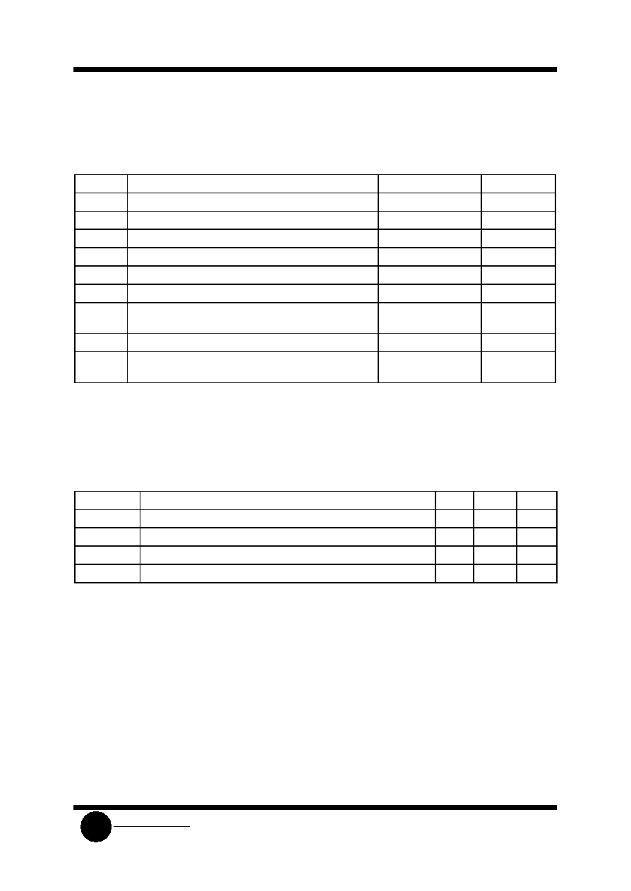
MAXIMUM RATINGS
*
Symbol
Parameter
Value
Unit
V
CC
DC Supply Voltage (Referenced to GND)
-0.5 to +7.0
V
V
IN
DC Input Voltage (Referenced to GND)
-1.5 to V
CC
+1.5
V
V
OUT
DC Output Voltage (Referenced to GND)
-0.5 to V
CC
+0.5
V
I
IN
DC Input Current, per Pin
±
20
mA
I
OUT
DC Output Current, per Pin
±
25
mA
I
CC
DC Supply Current, V
CC
and GND Pins
±
50
mA
P
D
Power Dissipation in Still Air, Plastic DIP+
SOIC Package+
750
500
mW
Tstg
Storage Temperature
-65 to +150
∞
C
T
L
Lead Temperature, 1 mm from Case for 10 Seconds
(Plastic DIP or SOIC Package)
260
∞
C
*
Maximum Ratings are those values beyond whitch damage to the device may occur.
Functional operation should be restricted to the Recommended Operating Conditions.
+Derating - Plastic DIP: - 10 mW/
∞
C from 65
∞
to 125
∞
C
SOIC Package: : - 7 mW/
∞
C from 65
∞
to 125
∞
C
RECOMMENDED OPERATING CONDITIONS
Symbol
Parameter
Min
Max
Unit
V
CC
DC Supply Voltage (Referenced to GND)
4.5
5.5
V
V
IN
, V
OUT
DC Input Voltage, Output Voltage (Referenced to GND)
0
V
CC
V
T
A
Operating Temp erature, All Package Types
-55
+125
∞
C
t
r
, t
f
Input Rise and Fall Time (Figure 1)
0
500
ns
This device contains protection circuitry to guard against damage due to high static voltages or electric
fields. However, precautions must be taken to avoid applications of any voltage higher than maximum rated
voltages to this high-impedance circuit. For proper operation, V
IN
and V
OUT
should be constrained to the range
GND
(V
IN
or V
OUT
)
V
CC
.
Unused inputs must always be tied to an appropriate logic voltage level (e.g., either GND or V
CC
).
Unused outputs must be left open.
SL74HCT74
System Logic
Semiconductor
SLS
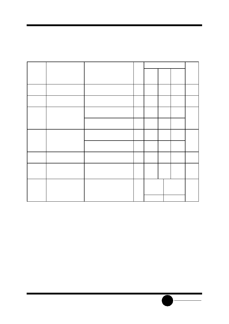
DC ELECTRICAL CHARACTERISTICS
(Voltages Referenced to GND)
V
CC
Guaranteed Limit
Symbol
Parameter
Test Conditions
V
25
∞
C
to
-55
∞
C
85
∞
C
125
∞
C
Unit
V
IH
Minimum High-Level
Input Voltage
V
OUT
=0.1 V or V
CC
-0.1 V
I
OUT
20
µ
A
4.5
5.5
2.0
2.0
2.0
2.0
2.0
2.0
V
V
IL
Maximum Low -Level
Input Voltage
V
OUT
=0.1 V or V
CC
-0.1 V
I
OUT
20
µ
A
4.5
5.5
0.8
0.8
0.8
0.8
0.8
0.8
V
V
OH
Minimum High-Level
Output Voltage
V
IN
=V
IH
or V
IL
I
OUT
20
µ
A
4.5
5.5
4.4
5.4
4.4
5.4
4.4
5.4
V
V
IN
=V
IH
or V
IL
I
OUT
4.0 mA
4.5
3.98
3.84
3.7
V
OL
Maximum Low-Level
Output Voltage
V
IN
=V
IH
or V
IL
I
OUT
20
µ
A
4.5
5.5
0.1
0.1
0.1
0.1
0.1
0.1
V
V
IN
=V
IH
or V
IL
I
OUT
4.0 mA
4.5
0.26
0.33
0.4
I
IN
Maximum Input
Leakage Current
V
IN
=V
CC
or GND
5.5
±
0.1
±
1.0
±
1.0
µ
A
I
CC
Maximum Quiescent
Supply Current
(per Package)
V
IN
=V
CC
or GND
I
OUT
=0
µ
A
5.5
1.0
10
40
µ
A
I
CC
Additional Quiescent
Supply Current
V
IN
=2.4 V, Any One Input
V
IN
=V
CC
or GND, Other
Inputs
-55
∞
C
25
∞
C to
125
∞
C
mA
I
OUT
=0
µ
A
5.5
2.9
2.4

SL74HCT74
System Logic
Semiconductor
SLS
AC ELECTRICAL CHARACTERISTICS
(V
CC
=5.0 V
±
10%,C
L
=50pF,Input t
r
=t
f
=6.0 ns)
Guaranteed Limit
Symbol
Parameter
25
∞
C
to
-55
∞
C
85
∞
C
125
∞
C
Unit
f
max
Maximum Clock Frequency (50% Duty Cycle)
(Figures 1 and 4)
30
24
20
MHz
t
PLH
, t
PHL
Maximum Propagation Delay, Clock to Q or Q
(Figures 1 and 4)
24
30
36
ns
t
PLH
, t
PHL
Maximum Propagation Delay, Set or Reset to Q or Q
(Figures 2 and 4)
24
30
36
ns
t
TLH
, t
THL
Maximum Output Transition Time, Any Output
(Figures 1 and 4)
15
19
22
ns
C
IN
Maximum Input Capacitance
10
10
10
pF
Power Dissipation Capacitance (Per Enabled
Output)
Typical @25
∞
C,V
CC
=5.0 V
C
PD
Used to determine the no-load dynamic power
consumption:
P
D
=C
PD
V
CC
2
f+I
CC
V
CC
130
pF
TIMING REQUIREMENTS
(V
CC
=5.0 V
±
10%,C
L
=50pF,Input t
r
=t
f
=6.0 ns)
Guaranteed Limit
Symbol
Parameter
25
∞
C to-55
∞
C
85
∞
C
125
∞
C
Unit
t
su
Minimum Setup Time, Data to Clock
(Figure 3)
15
19
22
ns
t
h
Minimum Hold Time, Clock to Data
(Figure 3)
3
3
3
ns
t
rec
Minimum Recovery Time, Set or Reset
Inactive to Clock (Figure 2)
6
8
9
ns
t
w
Minimum Pulse Width, Clock (Figure
1)
15
19
22
ns
t
w
Minimum Pulse Width, Set or Reset
(Figure 2)
15
19
22
ns
t
r
, t
f
Maximum Input Rise and Fall Times
(Figure 1)
500
500
500
ns

SL74HCT74
System Logic
Semiconductor
SLS
Figure 1. Switching Waveforms
Figure 2. Switching Waveforms
Figure 3. Switching Waveforms
Figure 4. Test Circuit
EXPANDED LOGIC DIAGRAM