SMSC DS ≠ USB97C100
Rev. 01/03/2001
USB97C100
ADVANCE INFORMATION
Multi-Endpoint USB Peripheral Controller
FEATURES
High Performance USB Peripheral Controller
Engine
-
Integrated USB Transceiver
-
Serial Interface Engine (SIE)
-
8051 Microcontroller (MCU)
-
Patented Memory Management Unit (MMU)
-
4 Channel 8237 DMA Controller
(ISADMA)
-
4K Byte On Board USB Packet Buffer
-
Quasi-ISA Peripheral Interface
-
USB Bus Snooping Capabilities
-
GPIOs
Complete USB Specification 1.1 Compatibility
-
Isochronous, Bulk, Interrupt, and Control
Data Independently Configurable per
Endpoint
-
Dynamic Hardware Allocation of -Packet
Buffer for Virtual Endpoints
-
Multiple Virtual Endpoints (up to 16 TX, 16
RX Simultaneously)
-
Multiple Alternate Address Filters
-
Dynamic Endpoint Buffer Length
Allocation (0-1280 Byte Packets)
High Speed (12Mbps) Capability
MMU and SRAM Buffer Allow Buffer Optimization
and Maximum Utilization of USB Bandwidth
-
128 Byte Page Size
-
10 Pages Maximum per Packet
-
Up to 16 Deep Receive Packet Queue
-
Up to 5 Deep Transmit Packet Queue, per
Endpoint
-
Hardware Generated Packet Header
Records Each Packet Status Automatically
-
Simultaneous Arbitration Between MCU,
SIE, and ISA DMA Accesses
Extended Power Management
-
Standard 8051 "Stop Clock" Modes
-
Additional USB and ISA Suspend
Resume Events
-
Internal 8MHz Ring Oscillator for Immediate
Low Power Code Execution
-
24, 16, 12, 8, 4, and 2 MHz PLL Taps For on
the Fly MCU and DMA Clock Switching
-
Independent Clock/Power Management for
SIE, MMU, DMA and MCU
DMA Capability with ISA Memory
-
Four Independent Channels
-
Transfer Between Internal and External
Memory
-
Transfer Between I/O and Buffer Memory
-
External Bus Master Capable
External MCU Memory Interface
-
1M Byte Code and Data Storage via 16K
Windows
-
Flash, SRAM, or EPROM
-
Downloadable via USB, Serial Port, or ISA
Peripheral
Quasi-ISA Interface Allows Interface to New and
"Legacy" Peripheral Devices
-
1M ISA Memory Space via 4K MCU Window
-
64K ISA I/O Space via 256 Byte MCU
Window
-
4 External Interrupt Inputs
-
4 DMA Channels
-
Variable Cycle Timing
-
8 Bit Data Path
5V
or 3.3v Operation
On Board Crystal Driver Circuit
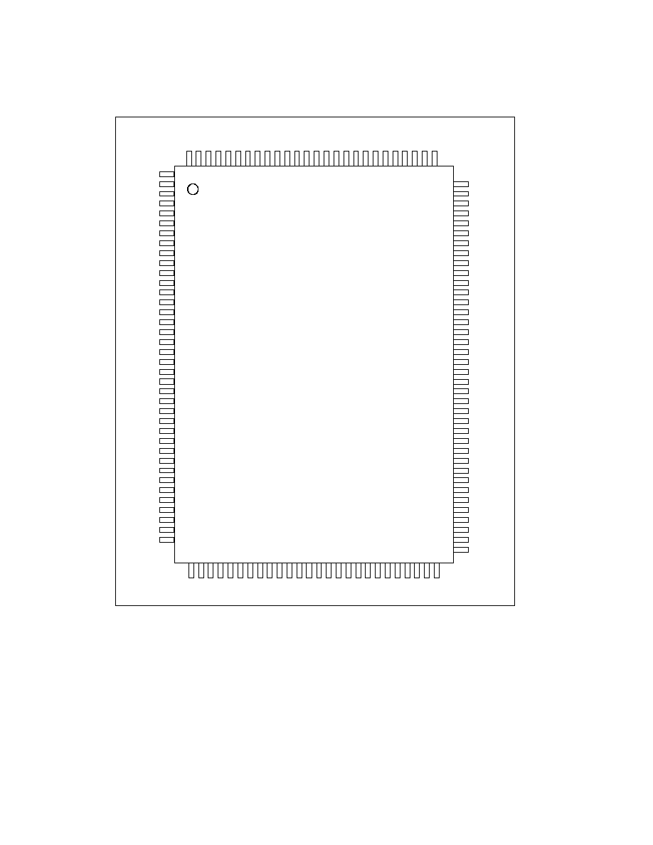
128 Pin QFP Package
ORDERING INFORMATION
Order Number: USB97C100QFP
128 Pin QFP Package

SMSC DS ≠ USB97C100
Page 2
Rev. 01/03/2001
GENERAL DESCRIPTION
The USB97C100 is a flexible, general purpose USB peripheral interface and controller ideally suited for multiple
endpoint applications. The USB97C100 provides an ISA-like bus interface, which will allow virtually any PC peripheral to
be placed at the end of a USB connection. Its unique dynamic buffer architecture overcomes the throughput
disadvantages of existing fixed FIFO buffer schemes allowing maximum utilization of the USB connection's overall
bandwidth. This architecture minimizes the integrated microcontroller's participation in the USB data flow, allowing back-
to-back packet transfers to block oriented devices. The efficiency of this architecture allows floppy drives to coexist with
other peripherals such as serial and parallel ports on a single USB link.
The USB97C100 allows external program code to be downloaded over the USB to allow easy implementation of varied
peripheral USB Device Classes and combinations. This also provides a method for convenient field upgrades and
modifications.
© STANDARD MICROSYSTEMS CORPORATION (SMSC) 2001
80 Arkay Drive
Hauppauge, NY 11788
(631) 435-6000
FAX (631) 273-3123
Standard Microsystems is a registered trademark of Standard Microsystems Corporation, and SMSC is a trademark of Standard Microsystems
Corporation. Product names and company names are the trademarks of their respective holders. Circuit diagrams utilizing SMSC products are included
as a means of illustrating typical applications; consequently complete information sufficient for construction purposes is not necessarily given. Although
the information has been checked and is believed to be accurate, no responsibility is assumed for inaccuracies. SMSC reserves the right to make
changes to specifications and product descriptions at any time without notice. Contact your local SMSC sales office to obtain the latest specifications
before placing your product order. The provision of this information does not convey to the purchaser of the semiconductor devices described any
licenses under the patent rights of SMSC or others. All sales are expressly conditional on your agreement to the terms and conditions of the most
recently dated version of SMSC's standard Terms of Sale Agreement dated before the date of your order (the "Terms of Sale Agreement"). The product
may contain design defects or errors known as anomalies which may cause the product's functions to deviate from published specifications. Anomaly
sheets are available upon request. SMSC products are not designed, intended, authorized or warranted for use in any life support or other application
where product failure could cause or contribute to personal injury or severe property damage. Any and all such uses without prior written approval of an
Officer of SMSC and further testing and/or modification will be fully at the risk of the customer. Copies of this document or other SMSC literature, as well
as the Terms of Sale Agreement, may be obtained by visiting SMSC's website at http://www.smsc.com.
SMSC DISCLAIMS AND EXCLUDES ANY AND ALL WARRANTIES, INCLUDING WITHOUT LIMITATION ANY AND ALL IMPLIED WARRANTIES
OF MERCHANTABILITY, FITNESS FOR A PARTICULAR PURPOSE, TITLE, AND AGAINST INFRINGEMENT, AND ANY AND ALL WARRANTIES
ARISING FROM ANY COURSE OF DEALING OR USAGE OF TRADE.
IN NO EVENT SHALL SMSC BE LIABLE FOR ANY DIRECT, INCIDENTAL, INDIRECT, SPECIAL, PUNITIVE, OR CONSEQUENTIAL DAMAGES,
OR FOR LOST DATA, PROFITS, SAVINGS OR REVENUES OF ANY KIND; REGARDLESS OF THE FORM OF ACTION, WHETHER BASED ON
CONTRACT, TORT, NEGLIGENCE OF SMSC OR OTHERS, STRICT LIABILITY, BREACH OF WARRANTY, OR OTHERWISE; WHETHER OR NOT
ANY REMEDY IS HELD TO HAVE FAILED OF ITS ESSENTIAL PURPOSE; AND WHETHER OR NOT SMSC HAS BEEN ADVISED OF THE
POSSIBILITY OF SUCH DAMAGES.
SMSC DS ≠ USB97C100
Page 5
Rev. 01/03/2001
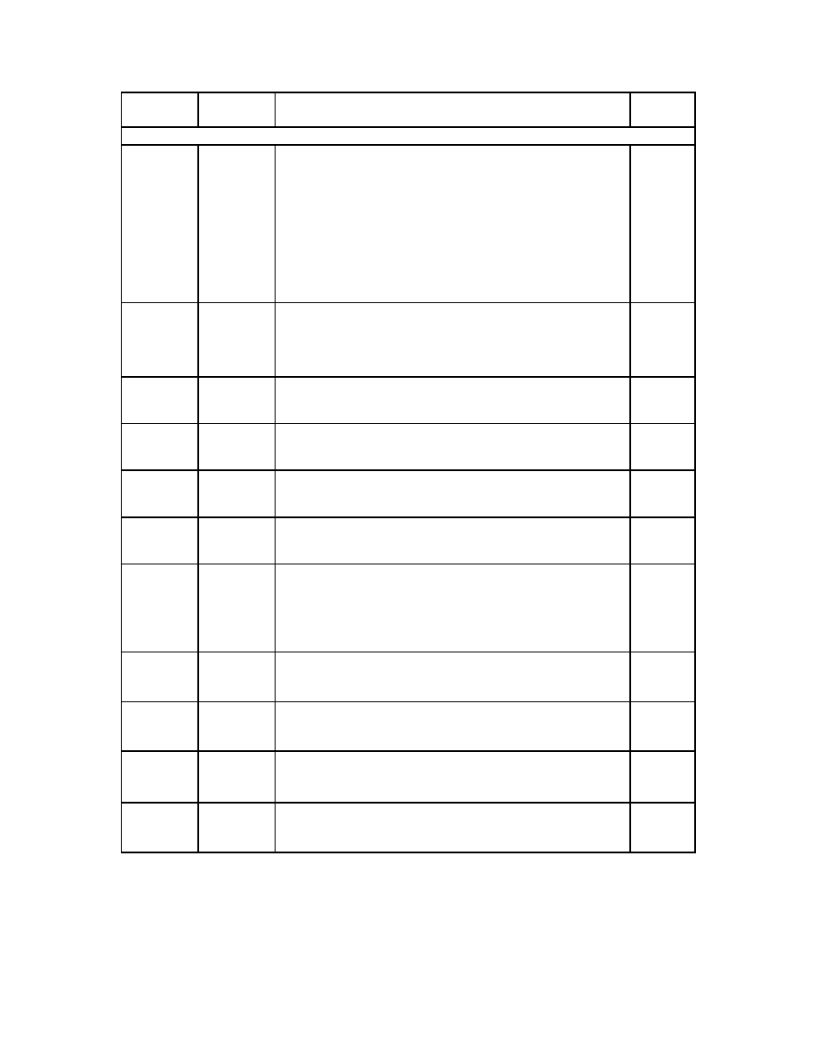
DESCRIPTION OF PIN FUNCTIONS
Table 1 - USB97C100 Pin Configuration
QFP PIN
NUMBER
SYMBOL
PIN DESCRIPTION
BUFFER
TYPE
ISA INTERFACE
100
READY
Channel is ready when high.
ISA memory or slave devices use this signal to lengthen a bus
cycle from the default time. Extending the length of the bus
cycle can only be done when the bus cycles are derived from
the Internal DMA controller core. 8051 MCU generated Memory
or I/O accesses cannot and will not be extended even if
READY is asserted low by an external ISA slave device. The
external slave device negates this signal after decoding a valid
address and sampling the command signals (nIOW, nIOR,
nMEMW, and nMEMR). When the slave's access has
completed, this signal should be allowed to float high.
IP
104, 106,
108, 110
DRQ[3:0]
DMA Request channels 3-0; active high.
These signals are used to request DMA service from the DMA
controller. The requesting device must hold the request signal
until the DMA controller drives the appropriate DMA
acknowledge signal (nDACK[3:0]).
I
105, 107,
109, 111
nDACK
[3:0]
DMA Acknowledge channels 3-0; active low.
These signals are used to indicate to the DMA requesting
device that it has been granted the ISA bus.
O8
103
TC
DMA Terminal Count; active high.
This signal is used to indicate that a DMA transfer has
completed.
O8
19-13,
127-7,
9-12
SA[19:0]
System Address Bus
These signals address memory or I/O devices on the ISA bus.
O8
112-115,
117-120
SD[7:0]
System Data Bus
These signals are used to transfer data between system
devices.
I/O8
122
AEN
Address Enable
This signal indicates address validation to I/O devices. When
low this signal indicates that an I/O slave may respond to
addresses and I/O commands on the bus. This signal is high
during DMA cycles to prevent I/O slaves from interpreting DMA
cycles as valid I/O cycles.
O8
123
nIOW
I/O Write; active low.
This signal indicates to the addressed ISA I/O slave to latch
data from the ISA bus.
O8
124
nIOR
I/O Read; active low.
This signal indicates to the addressed ISA I/O slave to drive
data on the ISA bus.
O8
125
nMEMR
Memory read; active low
This signal indicates to the addressed ISA memory slave to
drive data on the ISA bus.
O8
126
nMEMW
Memory write; active low
This signal indicates to the addressed ISA memory slave to
latch data from the ISA bus.
O8