 | –≠–ª–µ–∫—Ç—Ä–æ–Ω–Ω—ã–π –∫–æ–º–ø–æ–Ω–µ–Ω—Ç: SSD1730A | –°–∫–∞—á–∞—Ç—å:  PDF PDF  ZIP ZIP |

i
TABLE OF CONTENTS
1. GENERAL DESCRIPTION....................................................................................................................... 1
2. FEATURES............................................................................................................................................... 1
3. ORDERING INFORMATION .................................................................................................................... 1
5. FUNCTIONAL BLOCK DESCRIPTIONS................................................................................................. 3
6. PINS ASSIGNMENT................................................................................................................................. 4
7. PIN DESCRIPTION................................................................................................................................... 5
8. DC CHARACTERISTICS.......................................................................................................................... 8
10. AC CHARACTERISTICS...................................................................................................................... 10
11. EXPLANATION OF FUNCTIONS ........................................................................................................ 12
12. APPLICATION CIRCUIT (SSD1730 5X STEP-UP MODE) ................................................................ 17
13. PACKAGE DIMENSIONS .................................................................................................................... 18


SOLOMON SYSTECH
SEMICONDUCTOR TECHNICAL DATA
This document contains information on a new product under definition stage. Solomon Systech Limited reserves
the right to change or discontinue this product without notice.
http://www.solomon-systech.com
SSD1730
Rev 2.1
P 1
Feb 2003
Copyright
2003 Solomon Systech Limited
SSD1730
Advance Information
SSD1730 MLA Power Chip
CMOS
1. GENERAL DESCRIPTION
The SSD1730 is a power chip for operating four-line MLA (Multi Line Addressing) LCD drivers. It consists
of a CMOS charge pump-type voltage converter that can generate all the bias voltages required for the
four-line MLA drive based on a single power supply input.
SSD1730 can be used for the MLA system that is formed by a MLA column (segment) driver and a MLA
row (common) driver
(*)
. MLA display system is able to produce a module with lower power consumption
when comparing with the conventional driving method.
(*) Please refer to SSL MLA product list or application note for the MLA chipset product information.
2. FEATURES
Single Power Supply Operation,
+2.4V to +3.6V (5X step-up mode)
+2.4V to +3.0V (6X step-up mode)
Low current consumption
Two step-up modes, 5X or 6X step-up by internal charge pump DC/DC converter
Internal LCD voltage generator to generate all LCD voltages required for 4-line
MLA driving
External contrast control
Internal ≠V1 discharge circuit to discharge the residual charge at the row driver
negative voltage-side power supply voltage terminal ≠V1
Internal "power off" function using an external signal
Equipped internally with a LCD polarity reverse signal generator
Polarity reversed period in the range of 2P to 17P
Available in 48 pin QFP package (0.5 mm terminal pitch)
3. ORDERING INFORMATION
Ordering Part Number
Package Dimension
Package Form
SSD1730QL3
7 mm x 7mm
48 LQFP

Solomon Systech
Feb 2003
P 2
Rev 2.1
SSD1730
Table 1 - Ordering Information
4. BLOCK DIAGRAM
Column (Segment)
Driver Voltage Gener-
ator
Row (Common) Driver
Voltage Generator
LCD Polarity
Reverse Signal
Generator
Clock Signal
Generator
-V1 Discharge Circuit
C1P
C1N
C2P
C2N
-V3
C3P
C3N
V2
C4P
C4N
C1PB
C1NB
-V3B
HC
C5P
C5N
VEM
C6N
VEE
C8N
VDD_ROW
-V1
AB
XBB
L0
L1
L2
L3
FR
XFR
LP
XSLP
VDD_PWR
VSS
Row Driver Voltage
Conversion Circuit
VDD_ROW Voltage Generator
+V1 Voltage Generator
-V2
C7N
Figure 1 - Block Diagram

SSD1730
Rev 2.1
P 3
Feb 2003
Solomon Systech
5. FUNCTIONAL BLOCK DESCRIPTIONS
LCD Polarity Reverse Signal Generator
This circuit generates the polarity reverse signals FR and XFR from the pulse signal LP. The
polarity reversal interval is controlled by four pins L0, L1, L2 & L3 and the range is from 2P to 17P
(1P is equal to one LP period), Table 15 shows their relationship. The polarity of the FR signal and
the XFR signal are mutually opposite, so that the upper and lower screens can be driven mutually
in opposite phases when a two-screen drive panel is used.
Clock Signal Generator
This circuit generates the clock for the charge pump from the pulse signal LP. When the display
control signal XSLP is set to VSS, the clock will stop and the voltage converter will halt. For normal
display mode, XSLP must be tied to VDD_PWR. Besides, this circuit also generates the signals AB
& XBB which are the clocks for the column driver voltage generator and the row driver voltage
generator. Figure 7 shows their timing characteristics.
-V1 Discharge Circuit
When the display is off or the power is off, this circuit will discharge the residual charges at the
negative voltage level-side power supply voltage terminal ≠V1 of the row driver.
Column Driver Voltage Generator
This circuit accompanying with external components generates voltages for column driver. In
SSD1730, three voltage outputs including V2, -V2 and -V3 will be generated and their voltage
levels are based on the supply voltage VDD_PWR. Their relationship is V2 = VDD_PWR/2, -V2 = -
(VDD_PWR/2) and ≠V3 = -VDD_PWR.
Row Driver Voltage Generator
This voltage generator consists of three circuits (1) Row driver voltage conversion circuit, (2)
VDD_ROW voltage generator and (3) +V1 voltage generator.
Row Driver Voltage Conversion Circuit
This circuit generates VEE voltage which is used to generate +V1 & -V1 power supply voltages for
row driver. There are two step-up modes 5X and 6X which are set by the HC pin. When HC pin is
tied to VSS, 5X step-up mode is chosen. When HC pin is tied to -V3B, 6X step-up mode is chosen.
In SSD1730, VDD_PWR is taken as the reference, VEE is equal to -4 x VDD_PWR at 5X step-up
mode while VEE is equal to -5 x VDD_PWR at 6X step-up mode.
For the contrast adjustment, it is performed through the use of an external emitter follower circuit to
adjust VEE to generate ≠V1, this contrast control circuit is shown in Figure 9.
VDD_ROW Voltage Generator
VDD_ROW voltage generator is used to generate VDD_ROW, which is the power supply to the
logic circuit of a row driver.
+V1 Voltage Generator
+V1 voltage generator accompanies with an external MOS transistor to generate +V1 voltage,
which is required for the row driver. Figure 10 shows the accompanying external circuit for
generating +V1 voltage.

Solomon Systech
Feb 2003
P 4
Rev 2.1
SSD1730
6. PINS ASSIGNMENT
The package of SSD1730 is 48 LQFP and Table 2 shows its pin assignment.
Figure 2 - Pinout Diagram
Pin#
Signal Name
Pin#
Signal Name
Pin#
Signal Name
Pin#
Signal
Name
1 -V1 13 -V3B 25 NC2 37 L0
2 C8N 14
C1NB
26 NC
3 38 L1
3 VDD_ROW 15
VSS
27
-V3
39
L2
4 C7N 16 C1PB 28 C2P 40 L3
5
VSS
17 VDD_PWR 29 VDD_PWR 41 VSS
6 VEE 18 C4N 30 C1P 42 LP
7 C6N 19 -V2 31 VSS 43 FR
8 VEM 20 C4P 32 C3N 44
XFR
9 C5N 21 -V3 33 V2 45
XSLP
10 HC 22 VSS 34 NC4 46
XTST
11 NC1 23 C1N 35 C3P 47 AB
12 C5P 24 C2N 36
VDD_PWR
48
XBB
Table 2 - Pin Assignment Table
Pin 1

SSD1730
Rev 2.1
P 5
Feb 2003
Solomon Systech
7. PIN DESCRIPTION
Key:
I =Input
O =Output
I/O = Bi-Directional (Input/Output)
P = Power pin
NC = Dummy pin
Pin Name
Type
Pin#
Description
VDD_PWR
P
17, 29 & 36
Power supply pin
VSS
P
5, 15, 22, 31 & 41
Ground pin
Table 3 - Power Supply Pins
Pin Name
Type
Pin#
Description
L0 to L3
I
37 to 40
These input pins are used to set the polarity
reversal interval ranging from 2P to 17P.
FR
O
43
This is an output pin and the FR signal is
generated from the LCD polarity reverse signal
generator.
XFR
O
44
This is an output pin and the XFR signal is also
generated from the LCD polarity reverse signal
generator. This signal is a reverse phase from FR
signal.
Table 4 - Pins for frame signal generator
Pin Name
Type
Pin#
Description
LP
I
42
This input pin is used to generate the charge pump
clock and the polarity reverse signal FR and XFR.
A pulse signal with a period of 1P should be fed
into this pin.
XSLP
I
45
This input pin is used to switch on or off the
display. When it is set to VSS level, the clock and
the operations of the voltage converter will be stop.
The display will be off. When it is set to VDD_PWR
level, the display will be on.
Table 5 - Pins for clock signal generator

Solomon Systech
Feb 2003
P 6
Rev 2.1
SSD1730
Pin Name
Type
Pin#
Description
-V1
I/O
1
This is the row driver negative voltage level power
supply voltage terminal. The ≠V1 is an input signal
to the contrast adjustment circuit this is used to
adjust the display contrast. Besides, this is the
power supply to the +V1 voltage generator control
circuit.
Table 6 - Pins for ≠V1 discharge circuit
Pin Name
Type
Pin#
Description
C1P
I/O
30
The positive-side connection terminal for a
capacitor C1 to generate -V3 output voltage. (Refer
to the application circuit)
C1N
I/O
23
The negative-side connection terminal for a
capacitor C1 to generate -V3 output voltage. (Refer
to the application circuit)
C2P
I/O
28
The positive-side connection terminal for a
capacitor C2 to generate -V3 output voltage. (Refer
to the application circuit)
C2N
I/O
24
The negative-side connection terminal for a
capacitor C2 to generate -V3 output voltage. (Refer
to the application circuit)
-V3
O
21, 27
This is -V3 output voltage, which is for the power
supply of segment driver.
C3P
I/O
35
The positive-side connection terminal for a
capacitor C3 to generate V2 output voltage. (Refer
to the application circuit)
C3N
I/O
32
The negative-side connection terminal for a
capacitor C3 to generate V2 output voltage. (Refer
to the application circuit)
V2
I/O
33
This is V2 output voltage, which is for the power
supply of segment driver.
C4P
I/O
20
The positive-side connection terminal for a
capacitor C4 to generate -V2 output voltage. (Refer
to the application circuit)
C4N
I/O
18
The negative-side connection terminal for a
capacitor C4 to generate -V2 output voltage. (Refer
to the application circuit)
-V2
O
19
This is -V2 output voltage, which is for the power
supply of segment driver.
Table 7 - Pins for column (segment) driver voltage generator

SSD1730
Rev 2.1
P 7
Feb 2003
Solomon Systech
Pin Name
Type
Pin#
Description
Pins for VDD_ROW voltage generator
C8N
I/O
2
The negative-side connection terminal for a
capacitor C11 to generate VDD_ROW output
voltage. (Refer to the application circuit)
VDD_ROW
O
3
This is VDD_ROW output voltage, which is the
power supply to the logic circuit part of row driver.
Pins for +V1 voltage generator
AB
O
47
This is the clock output for the external n-channel
MOS transistor control in the +V1 voltage
generator circuit.
XBB
O
48
This is the clock output for the external p-channel
MOS transistor control in the +V1 voltage
generator circuit.
C7N
I/O
4
The negative-side connection terminal for a
capacitor C18 to generate +V1 output voltage.
(Refer to the application circuit)
Pins for row driver voltage conversion circuit
C1PB
I/O
16
The positive-side connection terminal for a
capacitor C10 and C11 to generate -V3B output
voltage. (Refer to the application circuit)
C1NB
I/O
14
The negative-side connection terminal for a
capacitor C10 to generate -V3B output voltage.
(Refer to the application circuit)
-V3B
O
13
This is -V3B output voltage equipped as the middle
voltage level for generating VEE output voltage.
HC
I
10
This pin is used to select 5X or 6X step-up mode.
When it is tied to VSS, 5X step-up mode will be
set. When it is tied to -V3B, 6X step-up mode will
be set.
C5P
I/O
12
The positive-side connection terminal for a
capacitor C8 and C9 to generate VEM output
voltage. (Refer to the application circuit)
C5N
I/O
9
The negative-side connection terminal for a
capacitor C8 to generate VEM output voltage.
(Refer to the application circuit)
VEM
O
8
This is VEM output voltage equipped as the middle
voltage level for generating VEE output voltage.
C6N
I/O
7
The negative-side connection terminal for a
capacitor C9 to generate VEE output voltage.
(Refer to the application circuit)
VEE
O
6
This is VEE output voltage.
Table 8 - Pins for row (common) driver voltage generator
Pin Name
Type
Pin#
Description
XTST
I
46
This is a test pin. This pin must be tied to the
VDD_PWR level in normal application.
NC1, NC2,
NC3, NC4
NC
11, 25, 26, 34
Dummy Pins. These pins must be left open &
unconnected in normal application.
Table 9 - Test circuit pins and Dummy pins

Solomon Systech
Feb 2003
P 8
Rev 2.1
SSD1730
8. DC CHARACTERISTICS
Maximum Ratings
Symbol
Parameter Value
Unit
VDD_PWR
Supply voltage (non-operation)
3.7
V
-V1
Row driver negative supply voltage
VEE≠0.3 to 0.3
V
V
in
Input voltage
-0.3 to VDD_PWR+3.0
V
VEE
Output voltage (min)
VDD_PWR-18
V
I
DD
Input current
10
mA
I
V2
Output current at V2
6
mA
I
-V2
Output current at -V2
6
mA
I
-V3
Output current at -V3
5
mA
I
VEE
Output current at VEE
1
mA
I
VDD_ROW
Output current at VDD_ROW
0.1
mA
T
A
Operating Temperature
-30 to +85
∞C
T
STG
Storage Temperature Range
-65 to +150
∞C
Table 10 - Maximum Ratings for DC characteristics (Voltage Referenced to VSS, T
A
=25∞C)
Maximum ratings are those values beyond which damage to the device may occur. Functional operation should be
restricted to the limits shown in the Electrical characteristics table.
This device contain circuitry to protect the inputs against damage due to high static voltages of electric
fields; however, it is advised that normal precautions to be taken to avoid application of any voltage
higher than maximum rated voltages to this high impedance circuit. All dummy pins and NC pins must be
left open & unconnected. Do not connect or group dummy pins or NC pins together.

SSD1730
Rev 2.1
P 9
Feb 2003
Solomon Systech
9. ELECTRICAL CHARACTERISTICS
Symbol Parameter
Test
Condition
Min
Typ
Max
Unit
VDD_PWR
Supply voltage range
(5X step-up mode)
(Absolute value referenced to VSS)
2.4
--
3.6
V
VDD_PWR
Supply voltage range
(6X step-up mode)
(Absolute value referenced to VSS)
2.4
--
3.0
V
-V1
Row driver negative
supply voltage Range
(Absolute value referenced to VSS)
VEE+0.6
--
-V3
V
I
std
Standby Mode Supply
Current Drain at
VDD_PWR
VDD_PWR=2.4V to 3.6V, Display off
(XSLP=V
IL
).
-- 2 5
µA
I
DP1
Display Mode Supply
Current Drain at
VDD_PWR in 5X step-up
mode
VDD_PWR=2.7V, 5X step-up, LP
period=69
µs, LP width=1µs, Display on
(XSLP=V
IH
), No loading
-- 270
380
µA
I
DP2
Display Mode Supply
Current Drain at
VDD_PWR in 6X step-up
mode
VDD_PWR=2.7V, 6X step-up, LP
period=69
µs, LP width=1µs, Display on
(XSLP=V
IH
), No loading
-- 350
480
µA
VDD_PWR
=2.7V
-13.5 -12.25 -- V
VEE
Output voltage at VEE
pin
6X step-up, LP period=69
µs, LP
width=1
µs, Display on
(XSLP=V
IH
), Io=0.4mA (from
VSS)
VDD_PWR
=2.4V
-12.0 -10.85 -- V
VDD_PWR
=2.7V
-- -V1+2.7 -- V
VDD_ROW
Output voltage at
VDD_ROW pin
6X step-up, LP period=69
µs, LP
width=1
µs, Display on
(XSLP=V
IH
), Io=0.02mA (to ≠
V1)
VDD_PWR
=2.4V
-- -V1+2.4 -- V
VDD_PWR
=2.7V
-- 1.313
1.35
V
V2
Output voltage at V2 pin
6X step-up, LP period=69
µs, LP
width=1
µs, Display on
(XSLP=V
IH
), Io=2mA (to VSS)
VDD_PWR
=2.4V
-- 1.16
1.20
V
VDD_PWR
=2.7V
-1.35 -1.276 -- V
-V2
Output voltage at -V2 pin
6X step-up, LP period=69
µs, LP
width=1
µs, Display on
(XSLP=V
IH
), Io=2mA (from
VSS)
VDD_PWR
=2.4V
-1.20 -1.134 -- V
VDD_PWR
=2.7V
-2.70 -2.646 -- V
-V3
Output voltage at -V3 pin
6X step-up, LP period=69
µs, LP
width=1
µs, Display on
(XSLP=V
IH
), Io=1mA (from
VSS)
VDD_PWR
=2.4V
-2.40 -2.352 -- V
V
IH
V
IL
Input High voltage at
pins: LP, XSLP, L0, L1,
L2, L3 and XTST
Input Low voltage at pins:
LP, XSLP, L0, L1, L2, L3
and XTST
VDD_PWR = 2.4V - 3.6V
0.8*VDD_PWR
0
--
--
VDD_PWR
0.2*VDD_PWR
V
V
OH
V
OL
Output High Voltage at
pins: XBB, AB, FR and
XFR
Output Low Voltage at
pins: XBB, AB, FR and
XFR
VDD_PWR = 2.4V - 3.6V, Iout=-20
µA
VDD_PWR-0.1
0
--
--
VDD_PWR
0.1
V
Table 11 - Electrical characteristics (Voltage Referenced to VSS, TA=25∞C)

Solomon Systech
Feb 2003
P 10
Rev 2.1
SSD1730
10. AC CHARACTERISTICS
Input Timing Characteristics
Symbol Parameter
Min
Typ
Max Unit
t
LPC
LP
Period
50
70 125 µs
t
LPW
LP
Width
70 1000 *2000 ns
t
LPr
LP Rise Time
--
--
10
ns
t
LPf
LP Fall Time
--
--
10
ns
Table 12 - Input Timing Characteristics (Voltage Referenced to VSS, VDD_PWR = 2.4 to 3.6V, T
A
=
25
∞C)
Remark *: It is noted that the wider the positive LP pulse with, the higher the output impedance of the
output voltage. The chip can function with positive LP pulse width in excess of 2000ns, but
high output impedance will be found.
t
L PW
t
L PC
t
LP r
t
L Pf
LP
Figure 3 - Timing Characteristics for input pin LP

SSD1730
Rev 2.1
P 11
Feb 2003
Solomon Systech
Output Timing Characteristics
LP pulse width = 1000ns, -V1 = VEE + 0.6V, 6X step-up mode application
Symbol Parameter
Min
Typ
Max Unit
t
FRr
FR/XFR Signal Rise Delay Time (with loading =
50pF)
330 -- 3300
ns
t
FRf
FR/XFR Signal Fall Delay Time (with loading =
50pF)
330 -- 3300
ns
t
ABr
AB Signal Rise Delay Time
230
--
2000
ns
t
Abf
AB Signal Fall Delay Time
180
--
1900
ns
t
XBBr
XBB Signal Rise Delay Time
130
--
1100
ns
t
XBBf
XBB Signal Fall Delay Time
280
--
3200
ns
t
OFFr
Rising Edge Output Phase Differential Time
1000
--
2400
ns
t
OFFf
Falling Edge Output Phase Differential Time
1000
--
2200
ns
t
C7Nr
C7N Signal Rising Edge Delay Time
270
--
2400
ns
t
C7Nf
C7N Signal Falling Edge Delay Time
490
--
3800
ns
Table 13 - Output Timing Characteristics
LP
FR
XFR
AB
XBB
t
F Rr
t
F Rf
t
ABr
t
XBB r
t
O F F r
t
C7 Nf
t
ABf
t
XBBf
t
OF F f
t
C 7N r
t
C 7N r
C7N
VSS
VL
VL
VSS
VSS-1.0V
VL+1.0V
t
C 7N f
Figure 4 - Output Timing Characteristics
-V1 -V1
-V1+1.0V

Solomon Systech
Feb 2003
P 12
Rev 2.1
SSD1730
11. EXPLANATION OF FUNCTIONS
This SSD1730 is a power chip for operating four-line MLA LCD drivers. It consists of a CMOS charge
pump-type voltage generator which can produce all of the bias voltages for a four-line MLA driven.
SSD1730 power chip can be used as a voltage generator to a display system formed by MLA column
driver and MLA row driver. In SSD1730, all output voltages are generated or reference from supply
power VDD_PWR. The voltage levels at 5X or 6X step-up mode can be calculated by the logical formulas
that are summarized in Table 14.
Figure 5 - Voltage levels relationship between power chip, column driver and row driver
5X Step-up Mode
6X Step-up Mode
Logical Formula
Voltage Level
(VDD_PWR=3.3V)
Logical Formula
Voltage Level
(VDD_PWR=3.0V)
+V1=-(-V1)
=4 x (VDD_PWR-VSS) -
13.2 -
+V1=-(-V1)
=5 x (VDD_PWR-VSS) -
15.0 -
V3=VDD_PWR-VSS
3.3
V3=VDD_PWR-VSS
3.0
V2=0.5 x (VDD_PWR-VSS)
1.65
V2=0.5 x (VDD_PWR-VSS)
1.5
VC=VSS 0.0
VC=VSS 0.0
-V2=-0.5 x (VDD_PWR-VSS)
-1.65
-V2=-0.5 x (VDD_PWR-VSS)
-1.5
-V3=-V3B=-(VDD_PWR-VSS) -3.3
-V3=-V3B=-(VDD_PWR-VSS) -3.0
VEM=-2 x (VDD_PWR-VSS)
-6.6
VEM=-3 x (VDD_PWR-VSS)
-9.0
VDD_ROW=-3 x (VDD_PWR-
VSS) +
-9.9 +
VDD_ROW=-4 x (VDD_PWR-
VSS) +
-12.0 +
-V1=-4 x (VDD_PWR-VSS) +
-13.2
+
-V1=-5 x (VDD_PWR-VSS) +
-15.0
+
VEE=-4 x (VDD_PWR-VSS)
-13.2
VEE=-5 x (VDD_PWR-VSS)
-15.0
Table 14 - Logical formula for SSD1730 (VSS = 0.0V)
Where
is a variable and it must greater than or equal to 0 ( 0). In practice, it represents contrast adjustment value.
SSD1730
Power Chip
MLA Row
Driver
MLA Column
Driver
External
components
VDD_PWR
VSS
VDD_PWR
V2
VSS
-V2
-V3
VDD_ROW
-V1
VEE
V3
V2
VSS
-V2
-V3
+V1
+V1
VC
VDD_ROW
-V1

SSD1730
Rev 2.1
P 13
Feb 2003
Solomon Systech
LCD Polarity Reverse Signal Generator
This circuit generates the polarity reverse signals FR and XFR from the 1P period pulse signal LP. The
polarity reversal period ranging from 2P to 17P is controlled by four pins L0, L1, L2 & L3. In such case,
the upper and lower screens can be driven in mutually opposite phases when a two-screen drive panel is
used, the polarity of the FR signal and the XFR signal are mutually opposite. The timing of the output
transitions is synchronized with the falling edge of the LP signal. Figure 6 shows the timing diagram of LP,
FR and XFR signals. Table 15 shows the relationship between the number of LP (NumLP) during the
frame interval and the settings of L0 to L3.
XSLP
FR
XF R
LP
1P Pe riod
N um LP
Num LP
Figure 6 - Timing Characteristics of LP, FR and XFR
L0 L1 L2 L3
Time
Number
Of
LP
(NumLP)
0 0 0 0
17P
LP
Signal
17
th
pulse
1 0 0 0 2P
LP
Signal
2
nd
pulse
0 1 0 0 3P
LP
Signal
3
rd
pulse
1 1 0 0 4P
LP
Signal
4
th
pulse
0 0 1 0 5P
LP
Signal
5
th
pulse
1 0 1 0 6P
LP
Signal
6
th
pulse
0 1 1 0 7P
LP
Signal
7
th
pulse
1 1 1 0 8P
LP
Signal
8
th
pulse
0 0 0 1 9P
LP
Signal
9
th
pulse
1 0 0 1
10P
LP
Signal
10
th
pulse
0 1 0 1
11P
LP
Signal
11
th
pulse
1 1 0 1
12P
LP
Signal
12
th
pulse
0 0 1 1
13P
LP
Signal
13
th
pulse
1 0 1 1
14P
LP
Signal
14
th
pulse
0 1 1 1
15P
LP
Signal
15
th
pulse
1 1 1 1
16P
LP
Signal
16
th
pulse
Table 15 - Relationship between NumLP and L0 to L3

Solomon Systech
Feb 2003
P 14
Rev 2.1
SSD1730
Clock Signal Generator
This circuit generates the clock for charge pump circuit from the pulse signal LP. When the display off
control signal XSLP is set to VSS, the clock will stop and the voltage converter will halt. The signal clocks
AB and XBB for the column driver voltage generator and the row driver voltage generator are also
generated by this circuit.
Input Signal XSLP
Input Signal LP
Output Signal AB
Output Signal XBB
Figure 7 - Timing diagram for LP, AB and XBB
Driver Voltage Generator
This circuit generates all voltage levels which are required to drive both the row driver and the column
driver. The voltage converter circuit comprises a CMOS charge pump-type DC/DC converter which is
formed by five individual voltage generator circuits including 1) Column driver voltage generator, 2) Row
driver voltage conversion circuit, 3) VDD_ROW voltage generator circuit, 4) +V1 voltage generator circuit
and 5) External contrast control circuit. Figure 8 shows the relationship between these voltage generator
circuits and Table 14 summarized all logical formulas which can be used to calculated these voltage
levels. Besides, in order to generate these voltages, external capacitors for the charge pump are
necessary. Application circuit shows their connections.
Figure 8 - Voltage generator control circuit
V3
V2
VC
-V2
-V3
VDD_ROW
+V1
VEE
-V1
Column driver
voltage
generator
VDD_ROW voltage
generator circuit
+V1 voltage generator
circuit
Ext. contrast
control circuit
Row driver
voltage
conversion
circuit
Row driver voltage generator
-V3B
VEM
VDD_PWR
VSS

SSD1730
Rev 2.1
P 15
Feb 2003
Solomon Systech
Contrast Control Circuit
The display contrast level ≠V1 is controlled by an external contrast adjustment circuit. Figure 9 shows the
typical connection of contrast control circuit.
-V3B
VL
VEE
S
S
D
17
30A
VL
2SA
500k
510k
Figure 9 - Typical connection of contrast control circuit
+V1 Voltage Generator
This circuit generates voltage level +V1 which is the positive power supply to row driver. Signal AB and XBB are the
clocks for this generator circuit. Figure 10 shows the typical connection of the +V1 voltage generator.
XBB
C7N
AB
S
S
D
1730A
VH
1.0uF
3.3M
2SJ
470pF
1.0pF
2SJ
Figure 10 - Typical connection of +V1 voltage generator
-V1
-V1
+V1

Solomon Systech
Feb 2003
P 16
Rev 2.1
SSD1730
-V1 and +V1 Discharge Circuit
When XSLP is set to VSS level, the internal ≠V1 discharge circuit will be triggered and the residual
charge at the row driver negative voltage-side power supply voltage terminal ≠V1 will be discharged to
the VSS level. However, the residual charge at the row driver positive voltage-side power supply terminal
+V1 can be discharged to the VSS level through an external MOS transistor. Figure 11 shows the typical
connection of the +V1 discharge circuit.
XSLP
VSS
S
S
D
1
7
30A
3.3M
2SK
2SK
VH
Figure 11 - Typical connection of +V1 discharge circuit
Power Up and Power Down Sequence
Proper power up sequence and power down sequence are recommended to protect the display system
and to have better performance.
Power Up Sequence:
Start ≠ Turn on the logic system in the application and power up the SSD1730
Display off ≠ Set Column and Row Driver DOFF# to "L"
Initialization ≠ Send LP, YD, XSCL and Data
Stable ≠ Wait for the power levels getting stable (around 80ms)
#
Display on ≠ Set Column and Row Driver DOFF# to "H"
Power Down Sequence:
Display off ≠ Set Column and Row Driver DOFF# to "L"
Sleep mode ≠ Set power chip to sleep mode by setting XSLP to "L"
Discharge ≠ Wait for the discharge of the display system (around 50ms)
#
Power down ≠ Cut the power of the SSD1730
End ≠ Turn off the logic system of the application
#
Depends on the system loading.
+V1

SSD1730
Rev 2.1
P 17
Feb 2003
Solomon Systech
12. APPLICATION CIRCUIT (SSD1730 5X Step-Up Mode)
VDD_ROW
-V1
+V1
500k
510k
2SA
3.3M
C17=470pF
2SJ
2SK
2SK
2SK
HC
-V3B
VEM
VDD_ROW
-V1
VEE
XBB
C7N
AB
C1P
C1N
C2P
C2N
C3P
C3N
C4P
C4N
V2
VSS
-V2
-V3
C5N
C5P
C6N
C1NB
C1PB
C8N
VDD=VDD_PW R
VSS
LP
XSLP
VDD
VSS
L3
L2
L1
L0
XTST
LP
XSLP
XFR
FR
XFR
V2
VC
-V2
-V3
C1=4.7uF
C2=4.7uF
C3=4.7uF
C4=4.7uF
C5=4.7uF
C6=4.7uF
C7=4.7uF
C10=4.7uF
C11=0.1uF
C8=1.0uF
C9=1.0uF
C18=1.0uF
C14=0.1uF
C13=1.0uF
C15=1.0uF
C16=1.0uF
C19=1.0uF
C12=4.7uF
3.3M
FR
V3
Figure 12 - Application Circuit for SSD1730 5X step-up mode
Remark: HC is tied to ≠V3B for 6X Step-up Mode.
Solomon Systech
Feb 2003
P 18
Rev 2.1
SSD1730
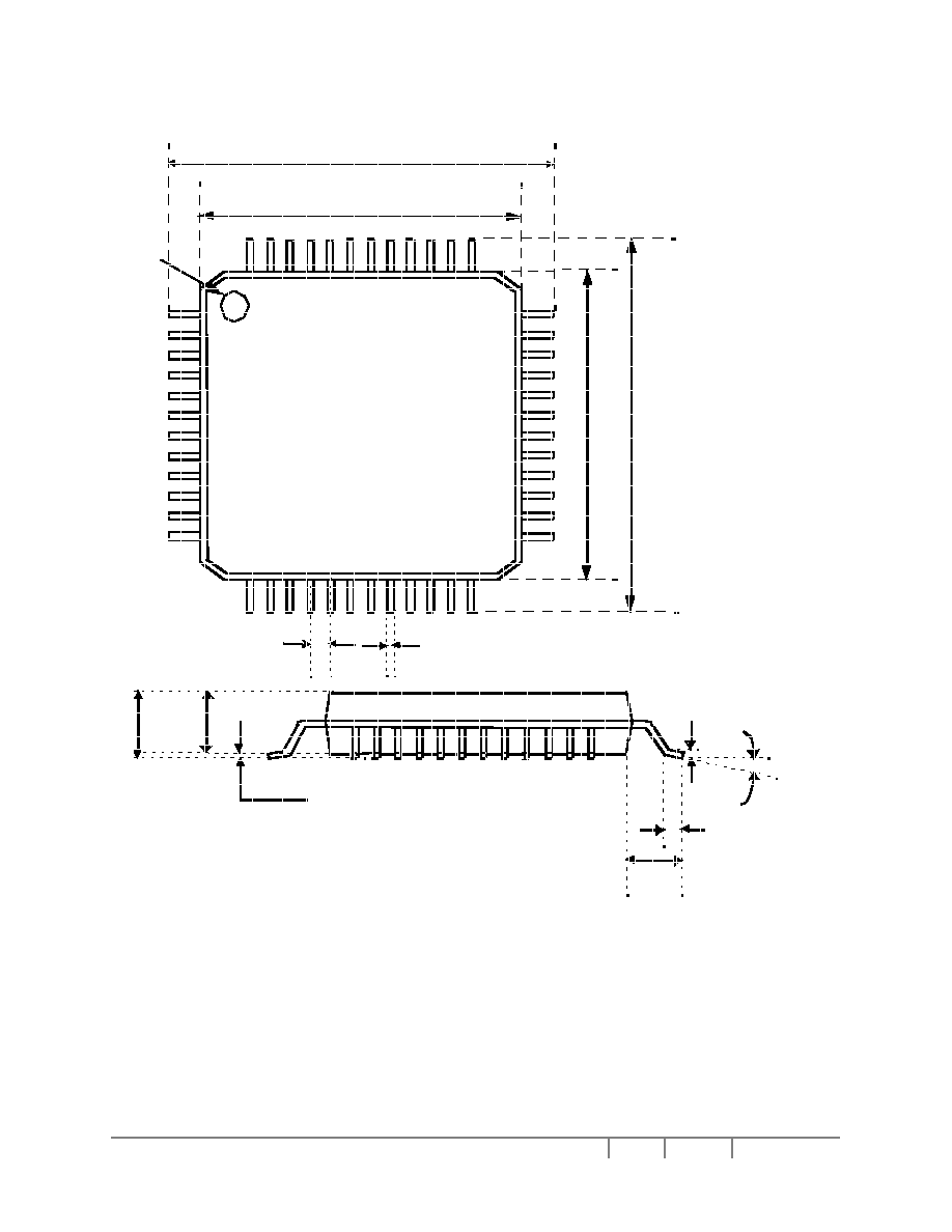
13. PACKAGE DIMENSIONS
1
12
13
24
25
36
48
7.
0
0
9.
0
0
7.00
9.00
0.22
±
0.05
0.50
Pin 1
Identifier
1.
6m
ax
1.
4
±
0.
05
min0.05
0.25
0.6 ±
0.15
1.00
48 LQFP
max0.15
3.5
o
±
3.5
(Dimension in mm, do not scale this drawing)
Figure 13 - Package Dimensions

SSD1730
Rev 2.1
P 19
Feb 2003
Solomon Systech
Solomon Systech reserves the right to make changes without further notice to any products herein. Solomon Systech makes no warranty,
representation or guarantee regarding the suitability of its products for any particular purpose, nor does Solomon Systech assume any liability arising
out of the application or use of any product or circuit, and specifically disclaims any and all liability, including without limitation consequential or
incidental damages. "Typical" parameters can and do vary in different applications. All operating parameters, including "Typicals" must be validated for
each customer application by customer's technical experts. Solomon Systech does not convey any license under its patent rights nor the rights of
others. Solomon Systech products are not designed, intended, or authorized for use as components in systems intended for surgical implant into the
body, or other applications intended to support or sustain life, or for any other application in which the failure of the Solomon Systech product could
create a situation where personal injury or death may occur. Should Buyer purchase or use Solomon Systech products for any such unintended or
unauthorized application, Buyer shall indemnify and hold Solomon Systech and its offices, employees, subsidiaries, affiliates, and distributors harmless
against all claims, costs, damages, and expenses, and reasonable attorney fees arising out of, directly or indirectly, any claim of personal injury or
death associated with such unintended or unauthorized use, even if such claim alleges that Solomon Systech was negligent regarding the design or
manufacture of the part.
http://www.solomon-systech.com