
This document contains information on a new product under definition stage. Solomon Systech Ltd. reserves the
right to change or discontinue this product without notice.
http://www.solomon-systech.com
SSD1820A/ 21
Rev 1.4
Jan 2003
Copyright
©
2003
Solomon Systech Limited
SSD1820A
SSD1821
ORDERING INFORMATION
SSD1820AZ
Gold Bump Die
SSD1821Z
Gold Bump Die
SSD1820ATR1 TAB
SSD1821TR1
TAB
Gold Bump Die
TAB
SOLOMON SYSTECH
SEMICONDUCTOR TECHNICAL DATA
P 1/43
Advance Information
LCD Segment / Common Driver
with Controller
CMOS
SSD1820A/21 is a single-chip CMOS LCD driver with controller for a liquid crystal
dot-matrix graphic display system. SSD1820A consists of 194 high voltage driving out-
put pins for driving 128 Segments, 64 Commons and 2 icon driving Commons, while
SSD1821 consists of 210 high voltage driving output pins for driving 128 Segments,
80 Commons and 2 icon driving Commons.
SSD1820A/21 displays data directly from its internal 128x65/128X81 bits Graphic
Display Data RAM (GDDRAM). Data/Commands are sent from general MCU through
a hardware selectable 6800-/8080-series compatible Parallel Interface or 3/4 wires
Serial Peripheral Interface.
SSD1820A/21 embeds a DC-DC Converter, a LCD Voltage Regulator, an On-
Chip Bias Divider and an On-Chip Oscillator which reduce the number of external
components. With the special design on minimizing power consumption and die/pack-
age layout, SSD1820A/21 is suitable for any portable battery-driven applications re-
quiring a long operation period and a compact size.
∑
128 x 64/80 Graphic Display with a Icon Line
∑
Programmable Multiplex ratio [16Mux - 65Mux/81Mux] (Partial Display)
∑
Single Supply Operation, 1.8 V - 3.3V
∑
Low Current Sleep Mode(<1.0uA)
∑
On-Chip Voltage Generator / External Power Supply
∑
Software selectable 2X / 3X / 4X / 5X / 6X On-Chip DC-DC Converter
∑
On-Chip Oscillator
∑
Software Selectable On-Chip Bias Dividers
∑
Programmable 1/4, 1/5, 1/6, 1/7, 1/8, 1/9 and 1/10 bias ratio
∑
Maximum +15.0V LCD Driving Output Voltage
∑
Hardware pin selectable for 8-bit 6800-series Parallel Interface, 8-bit 8080-series Par-
allel Interface, 3-wire Serial Peripheral Interface or 4-wire Serial Peripheral Interface
∑
On-Chip 128 x 65/81 Graphic Display Data RAM
∑
Re-mapping of Row and Column Drivers
∑
Vertical Scrolling
∑
Display Offset Control
∑
64 Levels Internal Contrast Control
∑
External Contrast Control
∑
Maximum 17MHz SPI or 15MHz PPI operation
∑
Selectable LCD Driving Voltage Temperature Coefficients (2 settings)
∑
Available in Gold Bump Die and Standard TAB (Tape Automated Bonding) Package

SSD1820A/ 21
Rev 1.4
Jan 2003
Solomon Systech
P 2/43
LCD Driving
Voltage Generator
2X / 3X / 4X / 5X /6X
DC/DC Converter,
Voltage Regulator,
Bias Divider,
Contrast Control,
Temperature
Compensation
COM0 to
COM63/79 SEG0~SEG127
V
SS
V
D D
D
7
VL6
V
CC
V
R
GDDRAM
128 X 65 Bits (SSD1820A)
128 x 81 Bits (SSD1821)
Command Decoder
Parallel / Serial Interface
Command Interface
Display
Timing
Generator
193 Bit Latch (SSD1820A)
209 Bit Latch (SSD 1821)
HV Buffer Cell Level Shifter
Level
Selector
Oscillator
D
6
D
5
D
4
D
3
D
2
D
1
D
0
(SDA)(SCK)
V
SS
Block Diagram
ICONS
REF
INTRS
V
C I
C
1P
C
2P
C
3P
C
4P
C
1N
C
2N
V
EXT
RES PS0 PS1
CS
D/C
R/W
E
VL5
VL4
VL3
VL2
(WR) (RD)
C
5P
CL

Solomon Systech
Jan 2003
Rev 1.4
SSD1820A/ 21
P 3/43
SSD1820ATR Pin Assignment
(Copper View)
N/C
PS1
/CS
/RES
D/C
R/W (/WR)
E (/RD)
D0
D1
D2
D3
D4
D5
D6
D7
VDD
VSS
VCC
C3P
C1N
C1P
C2P
C2N
NC
VL2
VL3
VL4
VL5
VL6
VR
CL
N/C
N/C
N/C
N/C
ICONS
COM63
COM62
:
:
:
:
:
:
COM33
COM32
N/C
SEG127
SEG126
:
:
:
:
:
:
SEG1
SEG0
ICONS
COM0
COM1
:
:
:
:
:
:
COM29
COM30
COM31
N/C
N/C
N/C
233
232
231
230
229
228
199
198
197
196
195
70
69
68
67
66
38
37
36
35
34
33
1
2
3
4
5
6
7
8
9
10
11
12
13
14
15
16
17
18
19
20
21
22
23
24
25
26
27
28
29
30
31
32
SSD1820AT Pin Assignment
(Copper View)
Note :
PS0, REF, INTRS and VCI are connected to VDD
Set condition:
Parallel interface, internal reference voltage, internal voltage regulator
and Booster reference voltage is VDD

SSD1820A/ 21
Rev 1.4
Jan 2003
Solomon Systech
P 4/43
SSD1821T Pin Assignment
(Copper View)
N/C
CL
VR
VL6
VL5
VL4
VL3
VL2
INTRS
C4P
C2N
C2P
C1P
C1N
C3P
C5P
VCC
VSS
VCI
VDD
D7(SDA)
D6(SCK)
D5
D4
D3
D2
D1
D0
E (/RD)
R/W (/WR)
D/C
/RES
/CS
PS1
PS0
N/C
N/C
COM39
COM38
COM37
COM36
:
:
:
:
:
:
COM1
COM0
ICONS
SEG0
SEG1
:
:
:
:
:
:
SEG125
SEG126
SEG127
COM40
COM41
:
:
:
:
:
:
COM75
COM76
COM77
COM78
COM79
ICONS
247
246
245
244
243
208
207
206
205
204
80
79
78
77
76
42
41
40
39
38
37
1
2
3
4
5
6
7
8
9
10
11
12
13
14
15
16
17
18
19
20
21
22
23
24
25
26
27
28
29
30
31
32
33
34
35
36
Note :
REF connected to VDD

Solomon Systech
Jan 2003
Rev 1.4
SSD1820A/ 21
P 5/43
N/C
N/C
:
N/C
CL
VSS
VR
VR
VL6
VL6
VL6
VL5
VL5
VL5
VL4
VL4
VL4
VL3
VL3
VL3
VL2
VL2
VL2
VSS
INTRS
VDD
VEXT
REF
VSS
C4P
C4P
C4P
C2N
C2N
C2N
C2N
C2P
C2P
C2P
C1P
C1P
C1P
C1N
C1N
C1N
C1N
C3P
C3P
C3P
N/C
N/C
N/C
VCC
VCC
VCC
VCC
VSS
VSS
VSS
VSS
VSS
VSS
VCI
VCI
VCI
VCI
VCI
VDD
VDD
VDD
D7 (SDA)
D7 (SDA)
D6 (SCK)
D6 (SCK)
D5
D4
D3
D2
D1
D0
VDD
E(/RD)
E(/RD)
R/W(/WR)
R/W(/WR)
VSS
D/C
D/C
D/C
/RES
VDD
/CS
/CS
VSS
PS1
VDD
VSS
PS0
VDD
N/C
N/C
:
:
N/C
N/C
COM5
COM4
COM3
COM2
COM1
COM0
ICONS
SEG0
SEG1
SEG2
SEG3
SEG4
SEG5
SEG6
SEG7
SEG8
SEG9
SEG10
SEG11
SEG12
SEG13
:
:
:
:
:
:
:
:
:
:
:
:
:
:
:
:
:
:
:
:
:
:
:
:
:
:
:
:
:
:
:
:
:
:
:
:
:
:
:
:
:
:
:
:
:
:
:
:
:
:
:
:
:
:
:
:
:
:
:
:
:
SEG113
SEG114
SEG115
SEG116
SEG117
SEG118
SEG119
SEG120
SEG121
SEG122
SEG123
SEG124
SEG125
SEG126
SEG127
COM32
COM33
COM34
COM35
COM36
COM37
COM38
N
/
C
C
O
M
3
9
C
O
M
4
0
C
O
M
4
1
C
O
M
4
2
:
: : :
: : :
: : :
:
C
O
M
6
1
C
O
M
6
2
C
O
M
6
3
I
C
O
N
S
N
/
C
Die Size: 10.8mm x 1.96mm
:
:
:
1
115
144
285
Die Thickness: 534um +/- 25um
Note:
1. Diagram showing the face of the die.
2. Coordinates are reference to center of the chip.
3. Unit of coordinates and Size of all alignment
marks are in um.
4. All alignment keys do not contain gold bump.
x
Y
(
0
,
0
)
Bump Height: 18um +/- 3um
SSD1820AZ Die Pin Assignment
N
/
C
C
O
M
6
C
O
M
7
C
O
M
8
C
O
M
9 : : : : : : : : : : :
C
O
M
2
8
C
O
M
2
9
C
O
M
3
0
C
O
M
3
1
N
/
C
Pin#1
DRAWING NOT TO SCALE

SSD1820A/ 21
Rev 1.4
Jan 2003
Solomon Systech
P 6/43
COM32
:
COM39
C L
VSS
VR
VR
VL6
VL6
VL6
VL5
VL5
VL5
VL4
VL4
VL4
VL3
VL3
VL3
VL2
VL2
VL2
VSS
INTRS
VDD
VEXT
REF
VSS
C4P
C4P
C4P
C2N
C2N
C2N
C2N
C2P
C2P
C2P
C1P
C1P
C1P
C1N
C1N
C1N
C1N
C3P
C3P
C3P
C5P
C5P
C5P
VCC
VCC
VCC
VCC
VSS
VSS
VSS
VSS
VSS
VSS
VCI
VCI
VCI
VCI
VCI
VDD
VDD
VDD
D7 (SDA)
D7 (SDA)
D6 (SCK)
D6 (SCK)
D 5
D 4
D 3
D 2
D 1
D 0
VDD
E(/RD)
E(/RD)
R/W(/WR)
R/W(/WR)
VSS
D/C
D/C
D/C
/RES
VDD
/CS
/CS
VSS
PS1
VDD
VSS
PS0
VDD
N/C
N/C
N/C
N/C
ICONS
COM79
:
COM73
COM5
COM4
COM3
COM2
COM1
COM0
ICONS
SEG0
SEG1
SEG2
SEG3
SEG4
SEG5
SEG6
SEG7
SEG8
SEG9
SEG10
SEG11
SEG12
SEG13
:
:
:
:
:
:
:
:
:
:
:
:
:
:
:
:
:
:
:
:
:
:
:
:
:
:
:
:
:
:
:
:
:
:
:
:
:
:
:
:
:
:
:
:
:
:
:
:
:
:
:
:
:
:
:
:
:
:
:
:
:
SEG113
SEG114
SEG115
SEG116
SEG117
SEG118
SEG119
SEG120
SEG121
SEG122
SEG123
SEG124
SEG125
SEG126
SEG127
COM40
COM41
COM42
COM43
COM44
COM45
COM46
N
/
C
C
O
M
4
7
C
O
M
4
8
C
O
M
4
9
C
O
M
5
0
:
: : :
: : :
: : :
:
C
O
M
6
9
C
O
M
7
0
C
O
M
7
1
C
O
M
7
2
N
/
C
Die Size: 10.8mm x 1.96mm
:
:
1
115
144
285
Die Thickness: 534um +/- 25um
Note:
1. Diagram showing the face of the die.
2. Coordinates are reference to center of the chip.
3. Unit of coordinates and Size of all alignment
marks are in um.
4. All alignment keys do not contain gold bump.
x
Y
(
0
,
0
)
Bump Height: 18um +/- 3um
SSD1821Z Die Pin Assignment
N
/
C
C
O
M
6
C
O
M
7
C
O
M
8
C
O
M
9 : : : : : : : : : : :
C
O
M
2
8
C
O
M
2
9
C
O
M
3
0
C
O
M
3
1
N
/
C
Pin#1
DRAWING NOT TO SCALE
Solomon Systech
Jan 2003
Rev 1.4
SSD1820A/ 21
P 7/43
Pin#1
(0,0)
X
Y
67.5um
22.5um 22.5um 22.5um
Center (-3926.1, 120)
x
22.5um
67.5um
Center (3991.5, 120)
x
99.9um
99.9um
Center (4409.4, -147.9)
x
78.75um
18.9um
78.75um
x
Center (-4095, -64.65)
Center (4263, -64.65)
Center (4515.6, -148.05)
70.875um
100.2um
52.2um
10.65um
51.9um
99.9um
49.8um
50.1um
10.98um
58.35um
x
2. Coordinates are reference to center of the chip
3. Unit of coordinates and Size of all alignment marks are in um.
4. All alignment keys do not contain gold bmup.
5. `X' represents the center point.
6. Drawing not to scale
Notes:
1. Diagram showing the gold bump view of the die.
SSD1820AZ & SSD1821Z Alignment Key Position

SSD1820A/ 21
Rev 1.4
Jan 2003
Solomon Systech
P 8/43
SSD1820A/21Z Die Pad Coordinates
Pad# SSD1820A SSD1821
x-pos
y-pos
Pad# SSD1820A SSD1821
x-pos
y-pos
Pad# SSD1820A SSD1821
x-pos
y-pos
Pad# SSD1820A SSD1821
x-pos
y-pos
1
N/C
COM73
-4568.40 -773.40
116
N/C
N/C
5191.50 -874.80
144
COM5
COM5
4568.40
773.40
286
N/C
N/C
-5191.50 874.80
2
N/C
COM74
-4503.60 -773.40
117
COM31
COM31
5191.50 -810.00
145
COM4
COM4
4503.60
773.40
287
COM39
COM47
-5191.50 810.00
3
N/C
COM75
-4438.80 -773.40
118
COM30
COM30
5191.50 -745.20
146
COM3
COM3
4438.80
773.40
288
COM40
COM48
-5191.50 745.20
4
N/C
COM76
-4374.00 -773.40
119
COM29
COM29
5191.50 -680.40
147
COM2
COM2
4374.00
773.40
289
COM41
COM49
-5191.50 680.40
5
N/C
COM77
-4309.20 -773.40
120
COM28
COM28
5191.50 -615.60
148
COM1
COM1
4309.20
773.40
290
COM42
COM50
-5191.50 615.60
6
N/C
COM78
-4244.40 -773.40
121
COM27
COM27
5191.50 -550.80
149
COM0
COM0
4244.40
773.40
291
COM43
COM51
-5191.50 550.80
7
N/C
COM79
-4179.60 -773.40
122
COM26
COM26
5191.50 -486.00
150
ICONS
ICONS
4179.60
773.40
292
COM44
COM52
-5191.50 486.00
8
N/C
ICONS
-4114.80 -773.40
123
COM25
COM25
5191.50 -421.20
151
SEG0
SEG0
4114.80
773.40
293
COM45
COM53
-5191.50 421.20
9
NC
NC
-3964.80 -807.45
124
COM24
COM24
5191.50 -356.40
152
SEG1
SEG1
4050.00
773.40
294
COM46
COM54
-5191.50 356.40
10
NC
NC
-3887.40 -807.45
125
COM23
COM23
5191.50 -291.60
153
SEG2
SEG2
3985.20
773.40
295
COM47
COM55
-5191.50 291.60
11
NC
NC
-3810.00 -807.45
126
COM22
COM22
5191.50 -226.80
154
SEG3
SEG3
3920.40
773.40
296
COM48
COM56
-5191.50 226.80
12
NC
NC
-3732.60 -807.45
127
COM21
COM21
5191.50 -162.00
155
SEG4
SEG4
3855.60
773.40
297
COM49
COM57
-5191.50 162.00
13
VDD
VDD
-3634.28 -807.45
128
COM20
COM20
5191.50
-97.20
156
SEG5
SEG5
3790.80
773.40
298
COM50
COM58
-5191.50
97.20
14
PS0
PS0
-3558.08 -807.45
129
COM19
COM19
5191.50
-32.40
157
SEG6
SEG6
3726.00
773.40
299
COM51
COM59
-5191.50
32.40
15
VSS
VSS
-3481.88 -807.45
130
COM18
COM18
5191.50
32.40
158
SEG7
SEG7
3661.20
773.40
300
COM52
COM60
-5191.50
-32.40
16
VDD
VDD
-3405.68 -807.45
131
COM17
COM17
5191.50
97.20
159
SEG8
SEG8
3596.40
773.40
301
COM53
COM61
-5191.50
-97.20
17
PS1
PS1
-3329.48 -807.45
132
COM16
COM16
5191.50
162.00
160
SEG9
SEG9
3531.60
773.40
302
COM54
COM62
-5191.50 -162.00
18
VSS
VSS
-3253.28 -807.45
133
COM15
COM15
5191.50
226.80
161
SEG10
SEG10
3466.80
773.40
303
COM55
COM63
-5191.50 -226.80
19
/CS
/CS
-3177.08 -807.45
134
COM14
COM14
5191.50
291.60
162
SEG11
SEG11
3402.00
773.40
304
COM56
COM64
-5191.50 -291.60
20
/CS
/CS
-3100.88 -807.45
135
COM13
COM13
5191.50
356.40
163
SEG12
SEG12
3337.20
773.40
305
COM57
COM65
-5191.50 -356.40
21
VDD
VDD
-3024.68 -807.45
136
COM12
COM12
5191.50
421.20
164
SEG13
SEG13
3272.40
773.40
306
COM58
COM66
-5191.50 -421.20
22
/RES
/RES
-2948.48 -807.45
137
COM11
COM11
5191.50
486.00
165
SEG14
SEG14
3207.60
773.40
307
COM59
COM67
-5191.50 -486.00
23
D/C
D/C
-2872.28 -807.45
138
COM10
COM10
5191.50
550.80
166
SEG15
SEG15
3142.80
773.40
308
COM60
COM68
-5191.50 -550.80
24
D/C
D/C
-2796.08 -807.45
139
COM9
COM9
5191.50
615.60
167
SEG16
SEG16
3078.00
773.40
309
COM61
COM69
-5191.50 -615.60
25
D/C
D/C
-2719.88 -807.45
140
COM8
COM8
5191.50
680.40
168
SEG17
SEG17
3013.20
773.40
310
COM62
COM70
-5191.50 -680.40
26
VSS
VSS
-2643.68 -807.45
141
COM7
COM7
5191.50
745.20
169
SEG18
SEG18
2948.40
773.40
311
COM63
COM71
-5191.50 -745.20
27
R/W
R/W
-2567.48 -807.45
142
COM6
COM6
5191.50
810.00
170
SEG19
SEG19
2883.60
773.40
312
ICONS
COM72
-5191.50 -810.00
28
R/W
R/W
-2491.28 -807.45
143
N/C
N/C
5191.50
874.80
171
SEG20
SEG20
2818.80
773.40
313
N/C
N/C
-5191.50 -874.80
29
E
E
-2415.08 -807.45
172
SEG21
SEG21
2754.00
773.40
30
E
E
-2338.88 -807.45
173
SEG22
SEG22
2689.20
773.40
31
VDD
VDD
-2262.68 -807.45
174
SEG23
SEG23
2624.40
773.40
32
D0
D0
-2186.48 -807.45
175
SEG24
SEG24
2559.60
773.40
33
D1
D1
-2110.28 -807.45
176
SEG25
SEG25
2494.80
773.40
34
D2
D2
-2034.08 -807.45
177
SEG26
SEG26
2430.00
773.40
35
D3
D3
-1957.88 -807.45
178
SEG27
SEG27
2365.20
773.40
36
D4
D4
-1881.68 -807.45
179
SEG28
SEG28
2300.40
773.40
37
D5
D5
-1805.48 -807.45
180
SEG29
SEG29
2235.60
773.40
38
D6
D6
-1729.28 -807.45
181
SEG30
SEG30
2170.80
773.40
39
D6
D6
-1653.08 -807.45
182
SEG31
SEG31
2106.00
773.40
40
D7
D7
-1576.88 -807.45
183
SEG32
SEG32
2041.20
773.40
41
D7
D7
-1500.68 -807.45
184
SEG33
SEG33
1976.40
773.40
42
VDD
VDD
-1424.48 -807.45
185
SEG34
SEG34
1911.60
773.40
43
VDD
VDD
-1348.28 -807.45
186
SEG35
SEG35
1846.80
773.40
44
VDD
VDD
-1272.08 -807.45
187
SEG36
SEG36
1782.00
773.40
45
VCI
VCI
-1149.90 -780.75
188
SEG37
SEG37
1717.20
773.40
46
VCI
VCI
-1073.70 -780.75
189
SEG38
SEG38
1652.40
773.40
47
VCI
VCI
-997.50 -780.75
190
SEG39
SEG39
1587.60
773.40
48
VCI
VCI
-921.30 -780.75
191
SEG40
SEG40
1522.80
773.40
49
VCI
VCI
-845.10 -780.75
192
SEG41
SEG41
1458.00
773.40
50
VSS
VSS
-768.90 -780.75
193
SEG42
SEG42
1393.20
773.40
51
VSS
VSS
-692.70 -780.75
194
SEG43
SEG43
1328.40
773.40
52
VSS
VSS
-616.50 -780.75
195
SEG44
SEG44
1263.60
773.40
53
VSS
VSS
-540.30 -780.75
196
SEG45
SEG45
1198.80
773.40
54
VSS
VSS
-464.10 -780.75
197
SEG46
SEG46
1134.00
773.40
55
VSS
VSS
-387.90 -780.75
198
SEG47
SEG47
1069.20
773.40
56
VCC
VCC
-311.70 -780.75
199
SEG48
SEG48
1004.40
773.40
57
VCC
VCC
-230.40 -780.75
200
SEG49
SEG49
939.60
773.40
58
VCC
VCC
-149.10 -780.75
201
SEG50
SEG50
874.80
773.40
59
VCC
VCC
-67.80 -780.75
202
SEG51
SEG51
810.00
773.40
60
NC
C5P
13.50 -780.75
203
SEG52
SEG52
745.20
773.40
61
NC
C5P
94.80 -780.75
204
SEG53
SEG53
680.40
773.40
62
NC
C5P
176.10 -780.75
205
SEG54
SEG54
615.60
773.40
63
C3P
C3P
257.40 -780.75
206
SEG55
SEG55
550.80
773.40
64
C3P
C3P
338.70 -780.75
207
SEG56
SEG56
486.00
773.40
65
C3P
C3P
420.00 -780.75
208
SEG57
SEG57
421.20
773.40
66
C1N
C1N
536.70 -780.75
209
SEG58
SEG58
356.40
773.40
67
C1N
C1N
612.90 -780.75
210
SEG59
SEG59
291.60
773.40
68
C1N
C1N
689.10 -780.75
211
SEG60
SEG60
226.80
773.40
69
C1N
C1N
765.30 -780.75
212
SEG61
SEG61
162.00
773.40
70
C1P
C1P
882.00 -780.75
213
SEG62
SEG62
97.20
773.40
71
C1P
C1P
963.30 -780.75
214
SEG63
SEG63
32.40
773.40

Solomon Systech
Jan 2003
Rev 1.4
SSD1820A/ 21
P 9/43
SSD1820A/21Z Die Pad Coordinates
72
C1P
C1P
1044.60 -780.75
215
SEG64
SEG64
-32.40
773.40
73
C2P
C2P
1125.90 -780.75
216
SEG65
SEG65
-97.20
773.40
74
C2P
C2P
1207.20 -780.75
217
SEG66
SEG66
-162.00
773.40
75
C2P
C2P
1288.50 -780.75
218
SEG67
SEG67
-226.80
773.40
76
C2N
C2N
1405.20 -780.75
219
SEG68
SEG68
-291.60
773.40
77
C2N
C2N
1481.40 -780.75
220 SEG69
SEG69
-356.40
773.40
78
C2N
C2N
1557.60 -780.75
221 SEG70
SEG70
-421.20
773.40
79
C2N
C2N
1633.80 -780.75
222
SEG71
SEG71
-486.00
773.40
80
C4P
C4P
1750.50 -780.75
223 SEG72
SEG72
-550.80
773.40
81
C4P
C4P
1831.80 -780.75
224 SEG73
SEG73
-615.60
773.40
82
C4P
C4P
1913.10
-780.75
225 SEG74
SEG74
-680.40
773.40
83
VSS
VSS
1989.30 -780.75
226 SEG75
SEG75
-745.20
773.40
84
REF
REF
2065.50 -780.75
227 SEG76
SEG76
-810.00
773.40
85
VEXT
VEXT
2182.20 -780.75
228 SEG77
SEG77
-874.80
773.40
86
VDD
VDD
2258.40 -780.75
229 SEG78
SEG78
-939.60
773.40
87
INTRS
INTRS 2334.60 -780.75
230 SEG79
SEG79
-1004.40
773.40
88
VSS
VSS
2410.80 -780.75
231 SEG80
SEG80
-1069.20
773.40
89
VL2
VL2
2487.00 -780.75
232
SEG81
SEG81
-1134.00
773.40
90
VL2
VL2
2568.30 -780.75
233 SEG82
SEG82
-1198.80
773.40
91
VL2
VL2
2649.60 -780.75
234 SEG83
SEG83
-1263.60
773.40
92
VL3
VL3
2730.90 -780.75
235 SEG84
SEG84
-1328.40
773.40
93
VL3
VL3
2812.20 -780.75
236 SEG85
SEG85
-1393.20
773.40
94
VL3
VL3
2893.50 -780.75
237 SEG86
SEG86
-1458.00
773.40
95
VL4
VL4
2974.80 -780.75
238 SEG87
SEG87
-1522.80
773.40
96
VL4
VL4
3056.10
-780.75
239 SEG88
SEG88
-1587.60
773.40
97
VL4
VL4
3137.40 -780.75
240 SEG89
SEG89
-1652.40
773.40
98
VL5
VL5
3218.70 -780.75
241 SEG90
SEG90
-1717.20
773.40
99
VL5
VL5
3300.00 -780.75
242
SEG91
SEG91
-1782.00
773.40
100
VL5
VL5
3381.30 -780.75
243 SEG92
SEG92
-1846.80
773.40
101
VL6
VL6
3462.60 -780.75
244 SEG93
SEG93
-1911.60
773.40
102
VL6
VL6
3543.90 -780.75
245 SEG94
SEG94
-1976.40
773.40
103
VL6
VL6
3625.20 -780.75
246 SEG95
SEG95
-2041.20
773.40
104
VR
VR
3741.90 -780.75
247 SEG96
SEG96
-2106.00
773.40
105
VR
VR
3818.10
-780.75
248 SEG97
SEG97
-2170.80
773.40
106
VSS
VSS
3894.30 -780.75
249 SEG98
SEG98
-2235.60
773.40
107
CL
CL
3970.50 -780.75
250 SEG99
SEG99
-2300.40
773.40
108
N/C
COM39
4114.80 -773.40
251 SEG100 SEG100
-2365.20
773.40
109
N/C
COM38 4179.60 -773.40
252 SEG101 SEG101 -2430.00
773.40
110
N/C
COM37 4244.40 -773.40
253 SEG102 SEG102
-2494.80
773.40
111
N/C
COM36 4309.20 -773.40
254 SEG103 SEG103
-2559.60
773.40
112
N/C
COM35 4374.00 -773.40
255 SEG104 SEG104
-2624.40
773.40
113
N/C
COM34 4438.80 -773.40
256 SEG105 SEG105
-2689.20
773.40
114
N/C
COM33 4503.60 -773.40
257 SEG106 SEG106
-2754.00
773.40
115
N/C
COM32 4568.40 -773.40
258 SEG107 SEG107
-2818.80
773.40
259 SEG108 SEG108
-2883.60
773.40
260 SEG109 SEG109
-2948.40
773.40
Bump size :
261 SEG110
SEG110
-3013.20
773.40
Pad 1~8, 108~115, 144~285 : 45x75um
262
SEG111
SEG111
-3078.00
773.40
Pad 9~107 :
52.2x60um
263 SEG112
SEG112
-3142.80
773.40
Pad 116~143, 286~313 :
75x45um
264 SEG113
SEG113
-3207.60
773.40
Tolerance : +/- 3um
265 SEG114
SEG114
-3272.40
773.40
Pad 1, 2, 3, ..... -> 115
266 SEG115
SEG115
-3337.20
773.40
267 SEG116
SEG116
-3402.00
773.40
268 SEG117
SEG117
-3466.80
773.40
269 SEG118
SEG118
-3531.60
773.40
270 SEG119
SEG119
-3596.40
773.40
271 SEG120 SEG120
-3661.20
773.40
272 SEG121 SEG121 -3726.00
773.40
273 SEG122 SEG122
-3790.80
773.40
274 SEG123 SEG123
-3855.60
773.40
275 SEG124 SEG124
-3920.40
773.40
276 SEG125 SEG125
-3985.20
773.40
277 SEG126 SEG126
-4050.00
773.40
278 SEG127 SEG127
-4114.80
773.40
279 COM32 COM40
-4179.60
773.40
280 COM33 COM41 -4244.40
773.40
281 COM34 COM42
-4309.20
773.40
282 COM35 COM43
-4374.00
773.40
283 COM36 COM44
-4438.80
773.40
284 COM37 COM45
-4503.60
773.40
285 COM38 COM46
-4568.40
773.40
SSD1820A /21
x
y

SSD1820A/ 21
Rev 1.4
Jan 2003
Solomon Systech
P 10/43
RES
This pin is reset signal input. When the pin is low, initialization of
the chip is executed.
PS0
This pin use together with PS1 to determine the interface proto-
col between the driver and MCU. Refer to PS1 pin descriptions for
more details.
PS1
This pin use together with PS0 to determine the interface proto-
col between the driver and MCU according to the following table.
CS
This pin is chip select input. The chip is enabled for display data/
command transfer only when CS is low.
D/C
This input pin is to identify display data/command cycle. When
the pin is high, the data written to the driver will be written into dis-
play RAM. When the pin is low, the data will be interpret as com-
mand. This pin must be connected to V
SS
when 3-lines SPI
interface is used.
R/W(WR)
This pin is microprocessor interface signal. When interfacing to
an 6800-series microprocessor, the signal indicates read mode
when high and write mode when low. When interfacing to an 8080-
microprocessor, a data write operation is initiated when R/W(WR)
is low and the chip is selected.
E(RD)
This pin is microprocessor interface signal. When interfacing to
an 6800-series microprocessor, a data operation is initiated when
E(RD) is high and the chip is selected. When interfacing to an
8080-microprocessor, a data read operation is initiated when
E(RD) is low and the chip is selected.
D
0
-D
7
These pins are 8-bit bi-directional data bus to be connected to
the microprocessor's data bus. When serial mode is selected, D
7
is
the serial data input SDA and D
6
is the serial clock input SCK.
INTRS
This pin is an input pin to enable the internal resistors network for
the voltage regulator when INTRS is high. When it is low, the exter-
nal resistors R
1
/R
2
should be connected to V
L6
, V
R
and V
SS
.
PS0
PS1
Interface
L
L
3-wire SPI (write only)
L
H
4-wire SPI (write only)
H
L
8080 parallel interface (read and write allowed)
H
H
6800 parallel interface (read and write allowed)
REF
This pin is an input pin to enable the internal reference voltage
used for the internal regulator. When it is high, an internal refer-
ence voltage source will be used. When it is low, an external refer-
ence voltage source must be provided in V
EXT
pin if internal
regulator is used.
V
DD
Power supply pin.
V
SS
Ground.
V
CI
Reference voltage input for internal DC-DC converter. The volt-
age of generated V
CC
equals to the multiple factor (2X, 3X, 4X, 5X
or 6X) times V
CI
with respect to V
SS
.
Note:
1.) voltage at this input pin must be larger than or equal to V
DD
.
2.) 6X is avaliable for SSD1821 only.
V
CC
This is the most positive voltage supply pin of the chip. It can be
supplied externally or generated by the internal DC-DC converter.
When using internal DC-DC converter as generator, voltage at
this pin is for internal reference only. It CANNOT be used for driv-
ing external circuitries.
C
1P
, C
2P
, C
3P
, C
4P
, C
5P
, C
1N
and C
2N
When internal DC-DC voltage converter is used, external
capacitor(s) is/are connected among these pins.
V
L6
This pin is the most positive LCD driving voltage. It can be sup-
plied externally or generated by the internal regulator.
V
R
This pin is an input of the internal voltage regulator. When the
internal resistors network for the voltage regulator is disabled
(INTRS is pulled low), external resistors should be connected
between V
SS
and V
R
, and V
R
and V
L6
, respectively (see applica-
tion circuit).
V
EXT
This pin is an input to provide an external voltage reference for
the internal voltage regulator when REF pin is pulled low.
PIN DESCRIPTIONS

Solomon Systech
Jan 2003
Rev 1.4
SSD1820A/ 21
P 11/43
V
L5
, V
L4
, V
L3
and V
L2
LCD driving voltages. They can be supplied externally or gener-
ated by the internal bias divider. They have the following relation-
ship:
V
L6
> V
L5
> V
L4
> V
L3
> V
L2
> V
SS
For SSD1820A, a equals to 9 at POR.
For SSD1821, a equal to 10 at POR.
COM0 - COM63/COM79
These pins provide the row driving signal COM0 - COM63/
COM79 to the LCD panel. See Table 1 or 2 about the COM signal
mapping in different multiplex ratio N.
ICONS
This pin is the special icons line COM signal output.
SEG0 - SEG127
These pins provide the LCD column driving signal. Their voltage
level is V
SS
during sleep mode and standby mode.
CL
This pin is the external clock input for the device which is
enabled by using an extended command. Under normal operation,
this pin should be left opened and internal oscillator will be used
after power on reset.
N/C
These No Connection pins should NOT be connected to any sig-
nal pins nor shorted together. They should be left open.
1:a bias
V
L5
(a-1)/a*V
L6
V
L4
(a-2)/a*V
L6
V
L3
2/a*V
L6
V
L2
1/a*V
L6

SSD1820A/ 21
Rev 1.4
Jan 2003
Solomon Systech
P 12/43
R/W(WR)
E(RD)
Figure 4: display data read with the insertion of dummy read
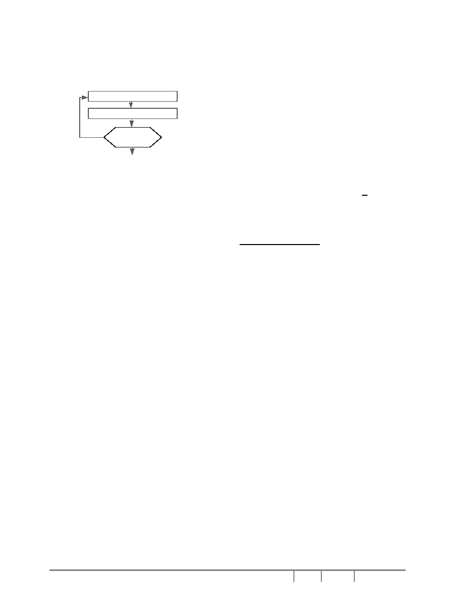
N
n
n+1
n+2
data bus
write column address
dummy read
data read1
data read 2
data read 3
Command Decoder and Command Interface
This module determines whether the input data is interpreted as data or
command. Data is directed to this module based upon the input of the D/C
pin. If D/C is high, data is written to Graphic Display Data RAM
(GDDRAM). If D/C is low, the input at D
0
-D
7
is interpreted as a Command
and it will be decoded and written to the corresponding command register.
Reset is of the same function as Power ON Reset (POR). Once RES
receives a negative reset pulse of about 1us, all internal circuitry will be
back to its initial status. Refer to Command Description section for more
information.
MPU Parallel 6800-series Interface
The parallel interface consists of 8 bi-directional data pins (D
0
-D
7
), R/
W(WR), D/C, E(RD) and CS. R/W(WR) input High indicates a read opera-
tion from the Graphic Display Data RAM (GDDRAM) or the status register.
R/W(WR) input Low indicates a write operation to Display Data RAM or
Internal Command Registers depending on the status of D/C input. The
E(RD) and CS input serves as data latch signal (clock) when they are high
and low respectively. Refer to Figure 1 of parallel timing characteristics for
Parallel Interface Timing Diagram of 6800-series microprocessors.
In order to match the operating frequency of display RAM with that of
the microprocessor, some pipeline processing is internally performed
which requires the insertion of a dummy read before the first actual display
data read. This is shown in Figure 4 below.
MPU Parallel 8080-series interface
The parallel interface consists of 8 bi-directional data pins (D
0
-D
7
), R/
W(WR), E(RD), D/C and CS. The CS input serves as data latch signal
(clock) when it is low. Whether it is display data or status register read is
controlled by D/C. R/W(W R) and E(RD) input indicates a write or read
cycle when CS is low. Refer to Figure 2 of parallel timing characteristics for
Parallel Interface Timing Diagram of 8080-series microprocessor.
Similar to 6800-series interface, a dummy read is also required before
the first actual display data read.
OPERATION OF LIQUID CRYSTAL DISPLAY DRIVER
Description of Block Diagram Module
MPU Serial 4-wire Interface
The serial interface consists of serial clock SCK, serial data SDA, D/
C and CS . SDA is shifted into a 8-bit shift register on every rising edge
of SCL in the order of D
7
, D
6
,... D
0
. D/C is sampled on every eighth
clock and the data byte in the shift register is written to the Display Data
RAM or command register in the same clock. No extra clock or com-
mand is required to end the transmission.
MPU Serial 3-wire Interface
Operation is similar to 4-wire serial interface while D/ C is not been
used. The Display Data Length instruction is used to indicate that a
specified number display data byte (1-256) are to be transmitted. Next
byte after the display data string is handled as a command.
It should be noted that if there is a signal glitch at SCK that causing
an out of synchronization in the serial communication, a hardware reset
pulse at RES pin is required to initialize the chip for re-synchronization.
Modes of operation
6800 parallel
8080 parallel
Serial
Data Read
Yes
Yes
No
Data Write
Yes
Yes
Yes
Command Read
Status only
Status only
No
Command Write
Yes
Yes
Yes
Segment and Common outputs are provided. For vertical scrolling of
display, an internal register storing the display start line can be set to
control the portion of the RAM data to be mapped to the display. Figure
5, 6 show the case in which the display start line register is set at 38H.
Graphic Display Data RAM (GDDRAM)
The GDDRAM is a bit mapped static RAM holding the bit pattern to be
displayed. The size of the RAM is 128 x 65 = 8320bits for SSD1820A; 128
x 81 = 10368bits for SSD1821. Figure 5, 6 are the description of the
GDDRAM address map. For mechanical flexibility, re-mapping on both

Solomon Systech
Jan 2003
Rev 1.4
SSD1820A/ 21
P 13/43
Page 7
Page 6
Page 5
Page 4
Page 3
Page 2
Page 1
Page 0
LSB
MSB
LSB
MSB
LSB
MSB
MSB
LSB
MSB
LSB
MSB
LSB
MSB
LSB
MSB [D7]
LSB [D0]
38H
COM0 (COM 63)
COM7 (COM56)
ICONS
COM63 (COM0)
COM8 (COM55)
SEG 0
SEG127
The configuration in parentheses represent the remapping of Rows and Columns
Note:
Figure 5. SSD1820A Graphic Display Data RAM (GDDRAM) Address Map (with vertical scroll value 38H)
Column address 00H
Column address 7FH
Page 8 (LSB)
COM SCAN MODE
NORMAL (REMAPPED)
(00H)
(7FH) Segment Remap Enabled
SSD1820A/ 21
Rev 1.4
Jan 2003
Solomon Systech
P 14/43
Page 7
Page 6
Page 5
Page 4
Page 3
Page 2
Page 1
Page 0
LSB
MSB
LSB
MSB
LSB
MSB
MSB
LSB
MSB
LSB
MSB
LSB
MSB
LSB
MSB [D7]
LSB [D0]
38H
COM0 (COM 79)
COM23 (COM56)
ICONS
COM79 (COM0)
COM24 (COM55)
SEG 0
SEG127
The configuration in parentheses represent the remapping of Rows and Columns
Note:
Figure 6. SSD1821 Graphic Display Data RAM (GDDRAM) Address Map (with vertical scroll value 38H)
Column address 00H
Column address 7FH
Page 10
COM SCAN MODE
NORMAL (REMAPPED)
(00H)
(7FH) Segment Remap Enabled
Page 9
Page 8
MSB
LSB
MSB
LSB
(LSB)

Solomon Systech
Jan 2003
Rev 1.4
SSD1820A/ 21
P 15/43
Figure 7. Oscillator Circuitry
LCD Driving Voltage Generator and Regulator
This module generates the LCD voltage needed for display output.
It takes a single supply input and generate necessary bias voltages.
It consists of:
1. 2X, 3X, 4X, 5X and 6X DC-DC voltage converter
Please refer to application notes.
Please note that SSD1820A works up to 5X and SSD1820AT
works up to 4X only.
2. Voltage Regulator
Feedback gain control for initial LCD voltage. External resistors
are connected between V
SS
and V
R
, and between V
R
and VL6.
These resistors are chosen to give the desired VL6 according to
the following equation:
where V
ref
is the internally generated reference voltage with a
known R
1
and R
2
. Typical value for V
ref
is 2.1V
R
1
is the resistance of the resistor between V
SS
and V
R
.
R
2
is the resistance of the resistors between V
R
and V
L6
.
is the software contrast level from 0 to 63.
G = 1 if INTRS = VDD; REF = VDD
G = 0.84 if INTRS = VSS; REF = VDD
3. Bias Divider
If the output op-amp buffer option in Set Power Control Register
command is enabled, this circuit block will divide the regulator output
(V
L6
) to give the LCD driving levels (V
L2
- V
L5
).
A low power consumption circuit design in this bias divider saves
most of the display current comparing to traditional design.
Stablizing Capacitors (0.47~2uF) are required to be connected
between these voltage level pins (V
L2
- V
L5
) and V
SS
. If the LCD panel
loading is heavy, capacitors and four additional resistors are suggest-
ref
con
V
V
◊
-
-
=
)
210
63
1
(
con
L
V
R
R
V
◊
+
=
)
1
(
1
2
6
G
◊
ref
con
V
V
◊
-
-
=
)
210
63
1
(
con
L
V
R
R
V
◊
+
=
)
1
(
1
2
6
G
◊
ed to add to the application circuit as follows:
Connections for heavy loading applications
4. Contrast Control
Software control of 64 voltage levels of LCD voltage.
5. Bias Ratio Selection circuitry
Software control of 1/ 4 to 1/10 bias ratio to match the characteris-
tic of LCD panel.
Note: SSD1820A has 1/4 to 1/9 bias only.
6. Self adjust temperature compensation circuitry
Provide 2 different compensation grade selections to satisfy the
various liquid crystal temperature grades. The grading can be
selected by software control. Defaulted temperature coefficient
(TC) value is -0.05% /
o
C for SSD1820A and -0.07%/
o
C for
SSD1821 .
193/209 Bit Latch
A register carries the display signal information. In 128 X 65/81 dis-
plamode. Data will be fed to the HV-buffer Cell and level-shifted to the
required level.
Level Selector
Level Selector is a control of the display synchronization. Display
voltage can be separated into two sets and used with different
cycles. Synchronization is important since it selects the required LCD
voltage level to the HV Buffer Cell, which in turn outputs the COM or
SEG LCD waveform.
SSD1820A/21 Series
Remarks: 1. C2 = 0.47 ~ 2.0uF
2. RL = 100K ~ 1M
V
SS
V
L2
V
L3
V
L4
V
L5
V
L6
RL
RL
RL
RL
+
V
SS
C2
+
C2
+
C2
+
C2
+
C2
Oscillator Circuit
This module is an On-Chip low power RC oscillator circuitry
(Figure 7). The oscillator generates the clock for the DC-DC voltage
converter. This clock is also used in the Display Timing Generator.
Oscillation Circuit
enable
OSC1
OSC2
Internal pwell resistor
Oscillator enable
Buffer
enable
(CL)

SSD1820A/ 21
Rev 1.4
Jan 2003
Solomon Systech
P 16/43
HV Buffer Cell (Level Shifter)
HV Buffer Cell works as a level shifter which translates the low
voltage output signal to the required driving voltage. The output is
shifted out with an internal FRM clock which comes from the Display
Timing Generator. The voltage levels are given by the level selector
which is synchronized with the internal M signal.
Reset Circuit
When RES input is low, the chip is initialized to the following:
1. Page address is set to 0
2. Column address is set to 0
3. Display is OFF
4. Display Start Line is set to 0 (GDDRAM page 0, D0)
5. Display Offset is set to 0 (COM0 is mapped to ROW0)
6. 128x64 for SSD1820A / 128x80 for SSD1821
7. Normal/Reverse Display is Normal
8. n-line Inversion Register is 0
9. Entire Display is OFF
10. Power Control Register (VC, VR, VF) is set to (0,0,0)
11. 2X/3X Booster is selected
12. Internal Resistor Ratio register is set to 0H
13. Software Contrast is set to 32
14. LCD Bias Ratio is set to 1/9 for SSD1820A and 1/10 for
SSD1821.
15. Normal scan direction of COM outputs
16. Segment remap is disabled (SEG0 display column address 0)
17. Internal oscillator is OFF
18. Test mode is OFF
19. Temperature coefficient is set to PTC0 for SSD1820A and
PTC1 for SSD1821.
20. Icon display line is OFF
21. Interface Lock / Unlock register will be clear
When RESET command is issued, the following parameters are
initialized only:
1. Page address is set to 0
2. Column address is set to 0
3. Initial Display Line is set to 0 (point to display RAM page 0, D0)
4. Internal Resistor Ratio register is set to 0H

Solomon Systech
Jan 2003
Rev 1.4
SSD1820A/ 21
P 17/43
TIME SLOT
COM0
COM1
SEG0
SEG1
M
* Note : N is the number of multiplex ratio including Icon line if it is enabled, N is equal to 64/80 on POR.
V
L6
V
L5
V
L4
V
L3
V
L2
V
SS
V
L6
V
L5
V
L4
V
L3
V
L2
V
SS
V
L6
V
L5
V
L4
V
L3
V
L2
V
SS
V
L6
V
L5
V
L4
V
L3
V
L2
V
SS
1 2 3 4 5 6 7 8 9
. . .
N
*
1 2 3 4 5 6 7 8 9
. . .
N
*
1 2 3 4 5 6 7 8 9
. . .
N
*
1 2 3 4 5 6 7 8 9
. . .
N
*
Figure 8a. LCD Display Example "0"
LCD Panel Driving Waveform
The following is an example of how the Common and Segment
drivers may be connected to a LCD panel. The waveforms shown in
Figure 8a and 7b illustrate the desired multiplex scheme with N-line
Inversion feature is disabled (default).
Figure 8b. LCD Driving Signal from SSD1820A/SSD1821
COM1
COM2
COM3
COM4
COM5
COM6
COM7
S
E
G
1
S
E
G
2
S
E
G
3
S
E
G
4
COM0
S
E
G
0

SSD1820A/ 21
Rev 1.4
Jan 2003
Solomon Systech
P 18/43
COMMAND TABLE
Hex
D7 D6 D5 D4 D3 D2 D1 D0 Command
Comment
00~0F
0
0
0
0
C3 C2 C1 C0 Set Lower Column Address
Sets the lower nibble of the column address pointer for
RAM access. The pointer is reset to 0 after reset.
10~17
0
0
0
1
0
C6 C5 C4 Set Upper Column Address
Sets the upper nibble of the column address pointer for
RAM access. The pointer is reset to 0 after reset.
18~1F
Reserved
Reserved
20~27
0
0
1
0
0
R2 R1 R0 Set Internal Regulator Resis-
tor Ratio
The internal regulator gain (1+R2/R1)Vcon increases as
R2R1R0 is increased from 000b to 111b. The resistor
ratio (1+R2/R1) is given by:
R2R1R0 = 000: 2.3 (POR)
R2R1R0 = 001: 3.0
R2R1R0 = 010: 3.7
R2R1R0 = 011: 4.4
R2R1R0 = 100: 5.1
R2R1R0 = 101: 5.8
R2R1R0 = 110: 6.5
R2R1R0 = 111: 7.2
28~2F
0
0
1
0
1
VC VR VF Set Power Control Register
VC=0: turns OFF the internal voltage booster (POR)
VC=1: turns ON the internal voltage booster
VR=0: turns OFF the internal regulator (POR)
VR=1: turns ON the internal regulator
VF=0: turns OFF the output op-amp buffer (POR)
VF=1: turns ON the output op-amp buffer
30~3F
Reserved
Reserved
40~43
0
x
1
L6
0
L5
0
L4
0
L3
0
L2
x
L1
x
L0
Set Display Start Line
The next command specifies the row address pointer
(0-63) of the RAM data to be displayed in COM0. This
command has no effect on COMS. The pointer is set to
0 after reset.
44~47
0
x
1
C6
0
C5
0
C4
0
C3
1
C2
x
C1
x
C0
Set Display Offset
The next command specifies the mapping of first display
line (COM0) to one of ROW0~63. This command has no
effect on COMS. COM0 is mapped to ROW0 after reset.
48~4B
0
x
1
D6
0
D5
0
D4
1
D3
0
D2
x
D1
x
D0
Set Multiplex Ratio
The next command specifies the number of lines,
excluding COMS, to be displayed. With Icon is disabled
(POR), duties 1/16~1/64 or 1/80 could be selected. With
Icon enabled, the available duty ratios are 1/17~ 1/65 or
1/81.
4C~4F
0
x
1
x
0
x
0
N4
1
N3
1
N2
x
N1
x
N0
Set N-line Inversion
The next command sets the n-line inversion register
from 3 to 33 lines to reduce display crosstalk. Register
values from 00001b to 11111b are mapped to 3 lines to
33 lines respectively. Value 00000b disables the N-line
inversion, which is the POR value.
To avoid a fix polarity at some lines, it should be noted
that the total number of mux (including the icon line)
should NOT be a multiple of the lines of inversion (n).
50~57
0
1
0
1
0
B2 B1
B 0 Set LCD Bias
Sets the LCD bias from 1/4 ~ 1/10 according to
B2B1B0:
000: 1/4 bias
001: 1/5 bias
010: 1/6 bias
011: 1/7bias
100: 1/8 bias
101: 1/9 bias (POR for SSD1820A)
110: 1/9 bias (for SSD1820A)
1/10 bias (POR for SSD1821)
111: 1/9 bias (for SSD1820A); 1/10 bias (for SSD1821)

Solomon Systech
Jan 2003
Rev 1.4
SSD1820A/ 21
P 19/43
58~63
Reserved
Reserved
64~67
0
1
1
0
0
1
B1 B0 Set DC-DC Conveter Factor
Sets the DC-DC multiplying factor from 2X to 6X B1B0:
00: 2X/3X (POR, 2X or 3X multiplying depended on the
DC-DC conveter configuration)
01: 4X
10: 5X (for SSD1820A)
11: 5X (for SSD1820A); 6X (for SSD1821)
68~80
Reserved
Reserved
81
1
x
0
x
0
C5
0
C4
0
C3
0
C2
0
C1
1
C0
Set Contrast Control Regis-
ter
The next command sets one of the 64 contrast levels.
The darkness increase as the contrast level increase.
The level is set to 32 after POR.
82~9F
Reserved
Reserved
A0~A1
1
0
1
0
0
0
0
S0 Set Segment Re-map
S0=0: column address 00H is mapped to SEG0 (POR)
S0=1: column address 7FH is mapped to SEG0
A2~A3
1
0
1
0
0
0
1
C0 Set Icon Enable
C0=0: Disable icon row (Mux = 16 to 64/80, POR)
C0=1: Enable icon row (Mux = 17 to 65/81)
A4~A5
1
0
1
0
0
1
0
E0 Set Entire Display On/Off
E0=0: Normal display (dispaly according to RAM con-
tents, POR)
E0=1: All pixels are ON regardless of the RAM contents
*Note: This command will override the effect of "Set
Normal/Reverse Display"
A6~A7
1
0
1
0
0
1
1
R0 Set Normal/Reverse Display
R0=0: Normal display (dispaly according to RAM con-
tents, POR)
R0=1: Reverse display (ON and OFF pixels are
inverted)
*Note: This command will not affect the display of the
icon lines
A8
Reserved
Reserved
A9
1
0
1
0
1
0
0
1
Set Power Save Mode
Enter Sleep mode
AA
Reserved
Reserved
AB
1
0
1
0
1
0
1
1
Start Internal Oscillator
Oscillator is OFF after reset, until this command is
issued. This command is required even if external oscil-
lator is used.
AE~AF
1
0
1
0
1
1
1
D0 Set Display On/Off
D0=0: Display OFF (POR)
D0=1: Display ON
B0~BF
1
0
1
1
P3 P2
P1 P0 Set Page Address
Set GDDRAM page address (0~10) using P3P2P1P0
for RAM access. The page address is sets to 0 after
reset.
C0~CF
1
1
0
0
S0 x
x
x
Set COM Output Scan
Direction
S0=0: Normal mode (POR)
S0=1: Remapped mode. COM0 to COM[N-1] becomes
COM[N-1] to COM0 when the duty is set to N.
See Figure 5/6 as an example for N equals to
64/80.
*Note: This command will not affect the display of the
icon lines
D0~E0
Reserved
Reserved
E1
1
1
1
0
0
0
0
1
Exit Power-save Mode
DC-DC converter, regulator and divider status before
entering the power-save mode is restored. At POR,
Power-save Mode is released.
E2
1
1
1
0
0
0
1
0
Software Reset
Initialize some internal registers
E3
Reserved
Reserved
E4
1
1
1
0
0
1
0
0
Exit N-line Inversion
The frame will be inverted once per frame
E5~E7
Reserved
Reserved

SSD1820A/ 21
Rev 1.4
Jan 2003
Solomon Systech
P 20/43
EXTENDED COMMAND TABLE
Read Status Byte
A 8 bits status byte will be placed to the data bus if a read operation is performed if D/C is low. The status byte is defined as follow.
Data Read / Write
To read data from the GDDRAM, input High to R/W(WR) pin and D/C pin for 6800-series parallel mode, Low to E(RD) pin and High to D/
C pin for 8080-series parallel mode. No data read is provided for serial mode. In normal mode, GDDRAM column address pointer will be
increased by one automatically after each data read. Also, a dummy read is required before the first data is read. See Figure 4 in Func-
E 8
1
D7
1
D6
1
D5
0
D4
1
D3
0
D2
0
D1
0
D0
Set Display Data Length
This command is valid only at 3-wire SPI (PS0=PS1=L)
The next command specifies the number of bytes of dis-
play data to be written after this composite command.
D(7:0)=00: 1 byte of display data is to be sent
D(7:0)=FF: 256 bytes of display data is to be sent
E9~EF
Reserved
Reserved
F0~FF
1
1
1
1
x
x
x
x
Extended Features
Test mode commands and Extended features, see
Extended Command Table.
Bit Pattern
Command
Comment
11110001
00001X
2
X
1
X
0
X
2
X
1
X
0
: Set TC Value
X
2
X
1
X
0
= 000: -0.05%/C (POR for 1820A)
X
2
X
1
X
0
= 001: -0.07%/C (POR for 1821)
11110010
0010X
3
X
2
X
1
X
0
X
3
: Select Oscillator Source
X
2
X
1
X
0
: Set Oscillator Value
X
3
= 0: Internal RC oscillator is selected (POR)
X
3
= 1: External oscillator from CL pin is selected
if X
3
= 0,
X
2
X
1
X
0
= 000: -16%
X
2
X
1
X
0
= 001: -10%
X
2
X
1
X
0
= 010: 0% (POR)
X
2
X
1
X
0
= 011: +10%
X
2
X
1
X
0
= 100: +16%
X
2
X
1
X
0
= 101: +30%
X
2
X
1
X
0
= 110: +54%
X
2
X
1
X
0
= 111: +81%
11111101
00010L10
L : Interface Lock / Unlock
L = 0 Interface Unlock (POR)
L = 1 Interface Lock
Other than above
Reserved
D7
D6
D5
D4
D3
D2
D1
D0
Comment
BUSY ON
RES
0
1
0
0
DS0
BUSY=0: Chip is idle
BUSY=1: Chip is executing instruction
ON=0: Display is OFF
ON=1: Dispaly is ON
RES=0: Chip is idlex
RES=1: Chip is executing reset
DS0=0: SSD1820A; DS0=1:SSD1821
Solomon Systech
Jan 2003
Rev 1.4
SSD1820A/ 21
P 21/43
tional Description.
To write data to the GDDRAM, input Low to R/W(W R) pin and High to D/ C pin for 6800-series parallel mode. For serial interface, it will
always be in write mode. GDDRAM column address pointer will be increased by one automatically after each data write. The address will
be reset to 0 in next data read/write operation is executed when it is 127.
Address Increment Table (Automatic)
Address Increment is done automatically after data read/write. The column address pointer of GDDRAM is also affected. It will be reset
to 0 in next data read/write operation is executed when it is 127.
Commands Required for R/W(WR) Actions on RAM
* No need to resend the command again if it is set previously.
The read / write action to the Display Data RAM does not depend on the display mode. This means the user can change the RAM content
whether the target RAM content is being displayed or not.
D/C
R/W(WR)
Comment
Address Increment
0
0
Write Command
No
0
1
Read Status
No
1
0
Write Data
Yes
1
1
Read Data
Yes
R/W(WR) Actions on RAMs
Commands Required
Read/Write Data from/to GDDRAM.
Set GDDRAM Page Address
Set GDDRAM Column Address
Read/Write Data
(1011X
3
X
2
X
1
X
0
)*
(0001X
3
X
2
X
1
X
0
)*
(0000X
3
X
2
X
1
X
0
)*
(X
7
X
6
X
5
X
4
X
3
X
2
X
1
X
0
)
SSD1820A/ 21
Rev 1.4
Jan 2003
Solomon Systech
P 22/43
Command Description
Set Display On/Off
This command turns the display on/off, by the value of the
LSB.
Set Display Start Line
This command is to set Display Start Line register to deter-
mine starting address of display RAM to be displayed by select-
ing a value from 0 to 63/79. With value equals to 0, D0 of Page 0
is mapped to COM0. With value equals to 1, D1 of Page0 is
mapped to COM0. The display start line values of 0 to 63/79 are
assigned to Page 0 to 7/9.
Set Page Address
This command positions the page address to 0 to 8/10 possi-
ble positions in GDDRAM. Refer to figure 5/6.
Set Higher Column Address
This command specifies the higher nibble of the 7-bit column
address of the display data RAM. The column address will be
incremented by each data access after it is pre-set by the MCU
and returning to 0 once overflow (>127).
Set Lower Column Address
This command specifies the lower nibble of the 7-bit column
address of the display data RAM. The column address will be
incremented by each data access after it is pre-set by the MCU
and returning to 0 once overflow (>127).
Set Segment Re-map
This commands changes the mapping between the display
data column address and segment driver. It allows flexibility in
layout during LCD module assembly. Refer to figure 5/6.
Set Normal/Reverse Display
This command sets the display to be either normal/reverse.
In normal display, a RAM data of 1 indicates an "ON" pixel while
in reverse display, a RAM data of 0 indicates an "ON" pixel. The
icon line is not affected by this command.
Set Entire Display On/Off
This command forces the entire display, including the icon
row, to be "ON" regardless of the contents of the display data
RAM. This command has priority over normal/reverse dis-
play.
To executed this command, Set Display On command
must be sent in advance.
Set LCD Bias
This command selects a suitable bias ratio (1/4 to 1/9 or
1/10) required for driving the particular LCD panel in use. The
POR default for SSD1820A is set to 1/9 bias; and 1/10 bias
for SSD1821.
Software Reset
This command causes some of the internal status of the
chip to be initialized:
1. Page address is set to 0
2. Column address is set to 0
3. Initial Display Line is set to 0 (point to display RAM page
0, D0)
4. Internal Resistor Ratio register is set to (0,0,0)
5. Software Contrast is set to 32
Set COM Output Scan Direction
This command sets the scan direction of the COM output
allowing layout flexibility in LCD module assembly.
Set Power Control Register
This command turns on/off the various power circuits asso-
ciated with the chip.
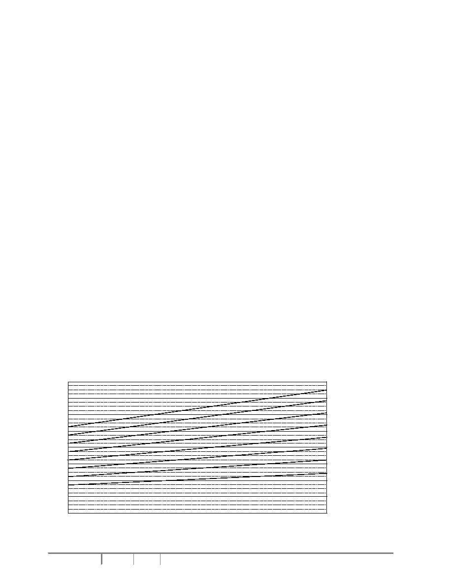
Set Internal Regulator Resistors Ratio
This command is to enable any one of the eight internal resis-
tor (IRS) settings for different regulator gains when using
internal regulator resistor network (INTRS pin pulled high).
When external resistors are used, INTRS must be connected
to VSS. The Contrast Control Voltage Range curves is given
in the figure below:
0.0
1 6 . 0
8.0
4.0
1 2 . 0
1 0 . 0
6.0
1 4 . 0
2.0
VL6 Voltage (V)
0
6 3
3 1
1 5
4 7
7
2 3
3 9
5 5
IRS
S e t t i n g
1 1 1
1 1 0
1 0 1
1 0 0
0 1 1
0 1 0
0 0 1
0 0 0
C o n t r a s t C o n t r o l S e t t i n g
D e f a u l t T C
Solomon Systech
Jan 2003
Rev 1.4
SSD1820A/ 21
P 23/43
Set Contrast Control Register
This command adjusts the contrast of the LCD panel by
changing VL6 of the LCD drive voltage provided by the On-Chip
power circuits. VL6 is set with 64 steps (6-bit) contrast control
register. It is a compound commands:
Set Display Offset
The next command specifies the mapping of display start line
(COM0 if display start line register equals to 0) to one of ROW0-
63/79. This command has no effect on COMS. COM0 is mapped
to ROW0 after reset.
Set Multiplex Ratio
This command switches default 64 multiplex mode to any mul-
tiplex from 16 to 64/80, if Icon is disabled (POR). When Icon is set
enable, the corresponding multiplex ratio setting will be mapped
to 17 to 65/81. The chip pads ROW0-ROW63/ROW79 will be
switched to corresponding COM signal output as specified in Ta-
ble 1 or 2.
Set Power Save Mode
To force the chip to enter Sleep Mode.
Exit Power Save Mode
This command releases the chip from Sleep Mode and return
to normal operation.
Set N-line Inversion
Number of line inversion is set by this command for reducing
crosstalk noise. 3 to 33-line inversion operations could be
selected. At POR, this operation is disabled.
It should be noted that the total number of mux (including the
icon line) should NOT be a multiple of the inversion number (n).
Or else, some lines will not change their polarity during frame
change.
Exit N-line Inverstion
This command releases the chip from N-line inversion mode.
The driving waveform will be inverted once per frame after issu-
ing this command.
Set DC-DC Converter Factor
Internal DC-DC converter factor is set by this command. For
SSD1820A, 2X to 5X multiplying factors could be selected. For
SSD1821, 2X to 6X mutiplying factors could be selected. 2X/3X,
4X, 5X and 6X factors are selected uising this command. Hard-
ware configuration is used for 2X or 3X setup.
Set Icon Enable
Set Contrast Control Register
Contrast Level Data
Changes
Complete?
No
Yes
This command enable/disable the Icon display.
Start InternalOscillator
After POR, the internal oscillator is OFF. It should be
turned ON by sending this command to the chip.
Set Display Data Length
This two-byte command only valid when 3-wire SPI config-
uration is set by H/W input (PS0=PS1=L). The second 8-bit is
used to indicate that a specified number display data byte (1-
256) are to be transmitted. Next byte after the display data
string is handled as a command.
Set Test Mode
This command force the driver chip into its test mode for
internal testing of the chip. Under normal operation, user
should NOT use this command.
Status register Read
This command is issued by setting D/C Low during a data
read (refer to figure 1 and 2 parallel interface waveform). It al-
lows the MCU to monitor the internal status of the chip. No sta-
tus read is provided for serial mode.
EXTENDED COMMANDS
These commands are used, in addition to basic commands, to
enable the enhanced features designed in the chips.
Set Temperature Coefficient (TC) Value
This command is to set 1 out of 2 different temperature
coefficients in order to match various liquid crystal tempera-
ture grades.
Enable external oscillator input.
This command enables the external clock input from CL
pin.
Select Oscillator Source
This command is used to adjust the oscillator frequency
to desire frame frequency.
Set Interface Lock / Unlock
After the interface lock command is issued, no more data or
commands will be accepted until an interface unlock com-
mand is issued.

SSD1820A/ 21
Rev 1.4
Jan 2003
Solomon Systech
P 24/43
MAXIMUM RATINGS*
(Voltages Referenced to V
SS
)
Symbol
Parameter
Value
Unit
V
DD
Supply Voltage
-0.3 to +4.0
V
V
CC
V
SS
-0.3 to V
SS
+15.0
V
V
CI
Booster Supply Voltage
V
DD
to +4.0
V
V
in
Input Voltage
V
SS
-0.3 to V
DD
+0.3
V
I
Current Drain Per Pin Excluding V
DD
and V
SS
25
mA
T
A
Operating Temperature
-40 to +85
∞C
T
stg
Storage Temperature Range
-65 to +150
∞C
* Maximum Ratings are those values beyond which damage to the device may occur. Functional
operation should be restricted to the limits in the Electrical Characteristics tables or Pin Descrip-
tion section.
This device contains circuitry to protect the inputs
against damage due to high static voltages or elec-
tric fields; however, it is advised that normal precau-
tions to be taken to avoid application of any voltage
higher than maximum rated voltages to this high
impedance circuit. For proper operation it is recom-
mended that V
in
a n d V
out
be constrained to the
range V
SS
< or = (V
in
or V
out
) < or = V
DD
. Reliability
of operation is enhanced if unused input are con-
nected to an appropriate logic voltage level (e.g.,
either V
SS
o r V
DD
). Unused outputs must be left
open. This device may be light sensitive. Caution
should be taken to avoid exposure of this device to
any light source during normal operation. This
device is not radiation protected.
ELECTRICAL CHARACTERISTICS
(Voltage Referenced to V
SS
, V
DD
=1.8 to 3.3V, T
A
=-40 to 85∞C; unless otherwise specified.)
Symbol
Parameter
Test Condition
Min
Typ (at 25∞C)
Max
Unit
V
DD
Logic Circuit Supply Voltage Range
Voltage Generator Circuit Supply Voltage Range
(Absolute value referenced to V
SS
)
1.8
2.7
3.3
V
I
AC
I
DP1
I
DP2
I
SB
I
SLEEP
Access Mode Supply Current Drain (V
D D
Pins
Display Mode Supply Current Drain (V
DD
Pins)
Display Mode Supply Current Drain (V
DD
Pins)
Standby Mode Supply Current Drain (V
DD
Pins)
Sleep Mode Supply Current Drain (V
DD
Pins)
V
DD
= 2.7V, Voltage Generator On, 4X Converter
Enabled, Write accessing, T
cyc
=3.3MHz, Osc.
Freq.=31kHz, Display On.
V
DD
= 2.7V, V
CC
= 10.8V, Voltage Generator Off,
external Divider Enabled. Read/Write Halt, Osc.
Freq. = 31kHz, Display On, VL6
= 9.0V.
V
DD
= V
CI
= 2.7V, V
CC
= 10.8V, Voltage Generator
On, 4x DC-DC Converter Enabled, V
CI
pin con-
nected to V
DD
. Internal Divider Enabled. Read/Write
Halt, Osc. Freq. = 31kHz, Display On, VL6 = 9.0V.
V
D D
=2.7V, LCD Driving Waveform Off, Osc. Freq. =
31kHz, Read/Write halt.
V
D D
= 2.7V, LCD Driving Waveform Off, Oscillator
Off, Read/Write halt.
-
-
-
-
-
300
15
90
8.0
0.5
600
26
120
37
3
µ
A
µ
A
µ
A
µ
A
µ
A
V
CC
V
LCD
LCD Driving Voltage Generator Output (V
C C
Pin)
DC-DC Converter Efficiency
LCD Driving Voltage Input (V
CC
Pin)
Display On, Voltage Generator Enabled, DC/DC
Converter Enabled, Osc. Freq.=31kHz, Regulator
Enabled, Divider Enabled.
I
CC
< 20uA
Voltage Generator Disabled.
V
DD
95
4.0
-
99
-
15.0
15.0
V
%
V
V
REF
External Reference Voltage Input
Internal Reference Voltage
Internal Reference Voltage Source Disable (REF
pin pulled Low), External Reference voltage input to
V
EXT
pin.
Internal Reference Voltage Source Enabled (REF
pin pulled High), V
EXT
pin NC.
2.04
2.10
2.10
2.16
V
V

Solomon Systech
Jan 2003
Rev 1.4
SSD1820A/ 21
P 25/43
* The formula for the temperature coefficient is:
V
OH1
V
OL1
VL6
VL6
Output High Voltage (D
0
-D
7
)
Output Low Voltage (D
0
-D
7
)
LCD Driving Voltage Source (VL6 Pin)
LCD Driving Voltage Source (VL6 Pin)
I
out
= +500
µ
A
I
out
= -500
µ
A
Regulator Enabled (VL6 voltage depends on Int/Ext
Contrast Control)
Regulator Disable
0.8*V
D
D
0
V
DD
-
-
-
-
Floating
V
D D
0.2*V
D
D
V
CC
-
0.5
-
V
V
V
V
V
IH1
V
IL1
Input high voltage
(RES, PS0, PS1, CS, D/C, R/W, D
0
-D
7
, REF,
INTRS)
Input Low voltage
(RES, PS0, PS1, CS, D/C, R/W, D
0
-D
7
, REF,
INTRS)
0.8*V
D
D
0
-
-
V
D D
0.2*V
D
D
V
V
V
L6
V
L5
V
L4
V
L3
V
L2
V
L6
V
L5
V
L4
V
L3
V
L2
LCD Display Voltage Output
(V
L6
, V
L5
, V
L4
, V
L3
, V
L2
Pins)\
LCD Display Voltage Inpu
(V
L6
, V
L5
, V
L4
, V
L3
, V
L2
Pins)
Bias Divider Enabled, 1:a bias ratio
Voltage reference to V
SS
, External Voltage Genera-
tor, Bias Divider Disabled
-
-
-
-
-
V
L5
V
L4
V
L3
V
L2
V
SS
V
L6
(a-1)/a*V
L6
(a-2)/a*V
L6
2/a*V
L6
1/a*V
L6
-
-
-
-
-
-
-
-
-
-
V
C C
V
L6
V
L5
V
L4
V
L3
V
V
V
V
V
V
V
V
V
V
I
OH
I
OL
I
O Z
Output High Current Source
(D
0
-D
7
)
Output Low Current Drain
(D
0
-D
7
)
Output Tri-state Current Drain Source
(D
0
-D
7
)
V
out
=V
DD
-0.4V
V
out
=0.4V
50
-
-1
-
-
-
-
-50
1
µ
A
µ
A
µ
A
I
IL
/I
I H
Input Current
(RES , PS0, PS1, CS , E, D/C, R/W, D
0
-D
7
,
REF, INTRS)
-1
-
1
µ
A
C
I N
Input Capacitance
(all logic pins)
-
5
7.5
pF
VL6
Variation of VL6 Output (1.8V < V
DD
< 3.0V)
Regulator Enabled, Internal Contrast Control
Enabled, Set Contrast Control Register = 0
-
±
2
-
%
PTC0
PTC1
Temperature Coefficient Compensation*
Temperature Coefficient 0
Temperature Coefficient 1
Voltage Regulator Enabled (POR for SSD1820A)
Voltage Regulator Enabled (POR for SSD1821)
-0.04
-0.06
-0.05
-0.07
-0.06
-0.08
%
%
TC(%)=
V
L6
at 50∞C - V
L6
at 0∞C
50∞C - 0∞C
X
1
V
L6
at 25∞C
X 100%

SSD1820A/ 21
Rev 1.4
Jan 2003
Solomon Systech
P 26/43
AC ELECTRICAL CHARACTERISTICS (T
A
=25∞C, Voltage referenced to V
SS
, V
DD
=V
CI
=2.7V, unless otherwise specified.)
Symbol
Parameter
Test Condition
Min
Typ(at 25∞C)
Max
Unit
F
OSC
Oscillation Frequency of Display Timing Generator
(SSD1820A/21)
Internal Oscillator Enabled
28.4
33
39
kHz
F
FRM
Frame Frequency
(SSD1820A)
Display ON, Set 128 x 64 Graphic Display
Mode, Icon Line Enabled.
POR Oscillator Settings
70
84.6
100
Hz
Frame Frequency
(SSD1821)
Display ON, Set 128 x 80 Graphic Display
Mode, Icon Line Enabled.
POR Oscillator Settings
70
81.5
100
Hz
F
OSC
6 x 65
F
OSC
5 x 81
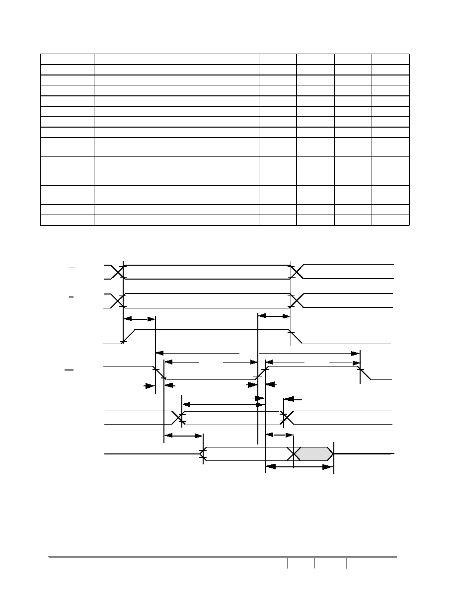
Solomon Systech
Jan 2003
Rev 1.4
SSD1820A/ 21
P 27/43
TABLE 3a. Parallel Timing Characteristics (T
A
=-40 to 85∞C, V
DD
=2.7V, V
SS
=0V)
Symbol
Parameter
Min
Typ
Max
Unit
t
cycle
Clock Cycle Time (write cycle)
66
-
-
ns
t
AS
Address Setup Time
0
-
-
ns
t
AH
Address Hold Time
0
-
-
ns
t
DSW
Write Data Setup Time
10
-
-
ns
t
DHW
Write Data Hold Time
2
-
-
ns
t
DHR
Read Data Hold Time
10
-
-
ns
t
O H
Output Disable Time
-
-
30
ns
t
ACC
Access Time (RAM)
Access Time (Command)
-
-
-
-
80
25
ns
ns
P W
CSL
Chip Select Low Pulse Width (read RAM)
Chip Select Low Pulse Width (read Command)
Chip Select Low Pulse Width (write)
95
40
15
-
-
-
-
ns
ns
PW
CSH
Chip Select High Pulse Width (read)
Chip Select High Pulse Width (write)
30
30
-
-
-
-
ns
ns
t
R
Rise Time
-
-
10
ns
t
F
Fall Time
-
-
10
ns
Valid Data
t
cycle
t
DSW
t
AS
t
AH
t
DHR
t
ACC
CS
D/C
D
0
-D
7
E
Valid Data
D
0
-D
7
(Write data to driver)
(Read data from driver)
t
DHW
PW
CSL
PW
CSH
t
F
t
R
R/W
t
O H
Figure 1a. Parallel 6800-series Interface Timing Characteristics (PS0 = H, PS1 = H)
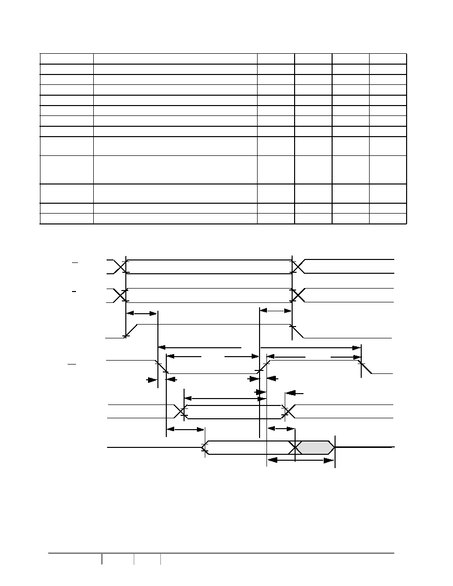
SSD1820A/ 21
Rev 1.4
Jan 2003
Solomon Systech
P 28/43
TABLE 3b. Parallel Timing Characteristics (T
A
=-40 to 85∞C, V
DD
=1.8V, V
SS
=0V)
Symbol
Parameter
Min
Typ
Max
Unit
t
cycle
Clock Cycle Time (write cycle)
80
-
-
ns
t
AS
Address Setup Time
0
-
-
ns
t
AH
Address Hold Time
0
-
-
ns
t
DSW
Write Data Setup Time
15
-
-
ns
t
DHW
Write Data Hold Time
5
-
-
ns
t
DHR
Read Data Hold Time
15
-
-
ns
t
O H
Output Disable Time
-
-
40
ns
t
ACC
Access Time (RAM)
Access Time (command)
-
-
-
-
100
35
ns
ns
P W
CSL
Chip Select Low Pulse Width (read RAM)
Chip Select Low Pulse Width (read Command)
Chip Select Low Pulse Width (write)
120
55
20
-
-
-
-
-
-
ns
ns
ns
PW
CSH
Chip Select High Pulse Width (read)
Chip Select High Pulse Width (write)
40
40
-
-
-
-
ns
ns
t
R
Rise Time
-
-
10
ns
t
F
Fall Time
-
-
10
ns
Valid Data
t
cycle
t
DSW
t
AS
t
AH
t
DHR
t
ACC
CS
D/C
D
0
-D
7
E
Valid Data
D
0
-D
7
(Write data to driver)
(Read data from driver)
t
DHW
PW
CSL
PW
CSH
t
F
t
R
R/W
t
O H
Figure 1b. Parallel 6800-series Interface Timing Characteristics (PS0 = H, PS1 = H)

Solomon Systech
Jan 2003
Rev 1.4
SSD1820A/ 21
P 29/43
TABLE 4a. Parallel Timing Characteristics (T
A
=-40 to 85∞C, V
DD
=2.7V, V
SS
=0V)
Symbol
Parameter
Min
Typ
Max
Unit
t
cycle
Clock Cycle Time (write cycle)
66
-
-
ns
t
AS
Address Setup Time
0
-
-
ns
t
AH
Address Hold Time
0
-
-
ns
t
DSW
Write Data Setup Time
10
-
-
ns
t
DHW
Write Data Hold Time
2
-
-
ns
t
DHR
Read Data Hold Time
10
-
-
ns
t
OH
Output Disable Time
-
-
30
ns
t
ACC
Access Time (RAM)
Access Time (Command)
-
-
-
-
80
25
ns
ns
PW
CSL
Chip Select Low Pulse Width (read RAM)
Chip Select Low Pulse Width (read Command)
Chip Select Low Pulse Width (write)
95
40
15
-
-
-
-
ns
ns
PW
CSH
Chip Select High Pulse Width (read)
Chip Select High Pulse Width (write)
30
30
-
-
-
-
ns
ns
t
R
Rise Time
-
-
10
ns
t
F
Fall Time
-
-
10
ns
Figure 2a. Parallel 8080-series Interface Timing Characteristics (PS0 = H, PS1 = L)
Valid Data
t
cycle
t
DSW
t
AS
t
AH
t
DHR
t
ACC
CS
D/C
D
0
-D
7
RD (E)
Valid Data
D
0
-D
7
(Write data to driver)
(Read data from driver)
t
DHW
PW
CSL
PW
CSH
t
F
t
R
t
O H
WR (R/W)

SSD1820A/ 21
Rev 1.4
Jan 2003
Solomon Systech
P 30/43
TABLE 4b. Parallel Timing Characteristics (T
A
=-40 to 85∞C, V
DD
=1.8V, V
SS
=0V)
Symbol
Parameter
Min
Typ
Max
Unit
t
cycle
Clock Cycle Time (write cycle)
80
-
-
ns
t
AS
Address Setup Time
0
-
-
ns
t
AH
Address Hold Time
0
-
-
ns
t
DSW
Write Data Setup Time
15
-
-
ns
t
DHW
Write Data Hold Time
5
-
-
ns
t
DHR
Read Data Hold Time
15
-
-
ns
t
OH
Output Disable Time
-
-
40
ns
t
ACC
Access Time (RAM)
Access Time (command)
-
-
-
-
100
35
ns
ns
PW
CSL
Chip Select Low Pulse Width (read RAM)
Chip Select Low Pulse Width (read Command)
Chip Select Low Pulse Width (write)
120
55
20
-
-
-
-
-
-
ns
ns
ns
PW
CSH
Chip Select High Pulse Width (read)
Chip Select High Pulse Width (write)
40
40
-
-
-
-
ns
ns
t
R
Rise Time
-
-
10
ns
t
F
Fall Time
-
-
10
ns
Valid Data
t
cycle
t
DSW
t
AS
t
AH
t
DHR
t
ACC
CS
D/C
D
0
-D
7
RD (E)
Valid Data
D
0
-D
7
(Write data to driver)
(Read data from driver)
t
DHW
PW
CSL
PW
CSH
t
F
t
R
t
O H
WR (R/W)
Figure 2b. Parallel 8080-series Interface Timing Characteristics (PS0 = H, PS1 = L)

Solomon Systech
Jan 2003
Rev 1.4
SSD1820A/ 21
P 31/43
TABLE 5a. Serial Timing Characteristics (T
A
=-40 to 85∞C, V
DD
=2.7V, V
SS
=0V)
Symbol
Parameter
Min
Typ
Max
Unit
t
cycle
Clock Cycle Time
59
-
-
ns
t
AS
Address Setup Time
10
-
-
ns
t
AH
Address Hold Time
5
-
-
ns
t
CSS
Chip Select Setup Time
10
-
-
ns
t
CSH
Chip Select Hold Time
5
-
-
ns
t
DSW
Write Data Setup Time
10
-
-
ns
t
DHW
Write Data Hold Time
10
-
-
ns
t
CLKL
Clock Low Time
10
-
-
ns
t
CLKH
Clock High Time
20
-
-
ns
t
R
Rise Time
-
-
10
ns
t
F
Fall Time
-
-
10
ns
Figure 3a. Serial Timing Characteristics (PS0 = L)
Valid Data
t
cycle
t
DSW
t
AS
t
AH
SCK
D/C
SDA
CS
t
DHW
t
CLKL
t
CLKH
t
F
t
R
t
CSS
t
CSH
(Required if PS1 = H)
D7
D6
D5
D4
D3
D2
D1
D0
SCK
SDA
CS

SSD1820A/ 21
Rev 1.4
Jan 2003
Solomon Systech
P 32/43
TABLE 5b. Serial Timing Characteristics (T
A
=-40 to 85∞C, V
DD
=1.8V, V
SS
=0V)
Symbol
Parameter
Min
Typ
Max
Unit
t
cycle
Clock Cycle Time
70
-
-
ns
t
AS
Address Setup Time
15
-
-
ns
t
AH
Address Hold Time
10
-
-
ns
t
CSS
Chip Select Setup Time
15
-
-
ns
t
CSH
Chip Select Hold Time
10
-
-
ns
t
DSW
Write Data Setup Time
15
-
-
ns
t
DHW
Write Data Hold Time
15
-
-
ns
t
CLKL
Clock Low Time
15
-
-
ns
t
CLKH
Clock High Time
30
-
-
ns
t
R
Rise Time
-
-
10
ns
t
F
Fall Time
-
-
10
ns
Figure 3b. Serial Timing Characteristics (PS0 = L)
Valid Data
t
cycle
t
DSW
t
AS
t
AH
SCK
D/C
SDA
CS
t
DHW
t
CLKL
t
CLKH
t
F
t
R
t
CSS
t
CSH
(Required if PS1 = H)
D7
D6
D5
D4
D3
D2
D1
D0
SCK
SDA
CS

Solomon Systech
Jan 2003
Rev 1.4
SSD1820A/ 21
P 33/43
SSD1821 DIE
(DIE FACE UP)
SEG0 -------------------------------- SEG127
DISPLAY PANEL SIZE
128 x 80 + 2 ICON LINES
80 MUX
Segment Remapped
[Command: A1]
D
0
-
D
7
R
/
W
C
S
R
E
S
D
/
C
V
S
S
V
C
C
I
N
T
R
S
External Vcc=10.8V
Remapped COM
SCAN Direction
[Command: C8]
Application Circuit: Bias divider enabled with external V
CC
.
VL2 VL3 VL4 VL5
VDD=2.7V
Optional for External
Resistors Gain Control
[INTRS pulled to VSS]
0.47
µ
F - 2.0
µ
F
R1
R2
VL6
VR
VSS
R
E
F
NC
COM6
COM7
:
:
:
COM20
COM19
:
:
:
COM30
COM31
NC
C
O
M
4
6
C
O
M
4
5
C
O
M
4
4
C
O
M
4
3
C
O
M
4
2
C
O
M
4
1
C
O
M
4
0
S
E
G
1
2
7
S
E
G
1
2
6
:
:
:
:
:
:
:
:
:
:
:
:
S
E
G
6
4
S
E
G
6
3
:
:
:
:
:
:
:
:
:
:
:
:
:
:
:
:
:
:
S
E
G
2
S
E
G
1
S
E
G
0
I
C
O
N
S
C
O
M
0
C
O
M
1
C
O
M
2
C
O
M
3
C
O
M
4
C
O
M
5
NC
COM47
COM48
:
:
:
COM52
COM53
:
:
:
COM71
COM72
NC
Remapped COM
SCAN Direction
[Command: C8]
COM40
:
COM47
COM48
:
COM73
COM74
:
COM79
ICONS
ICONS
COM0
:
COM6
COM7
:
COM32
COM33
:
COM39
Remapped COM
SCAN Direction
[Command: C8]
Remapped COM
SCAN Direction
[Command: C8]
C
O
M
7
3
:
:
C
O
M
7
9
I
C
O
N
S
C
O
M
3
9
:
:
C
O
M
3
3
C
O
M
3
2
Remapped COM
SCAN Direction
[Command: C8]
Remapped COM
SCAN Direction
[Command: C8]
E
See Application Notes
on P.35
Five captacitors and four
optional resistors for large
loading panel.
See description on P.15
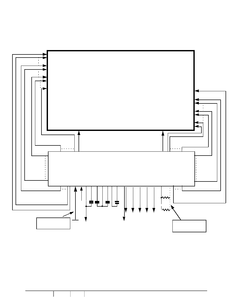
SSD1820A/ 21
Rev 1.4
Jan 2003
Solomon Systech
P 34/43
Application Circuit: 4X Booster, Bias divider disabled.
SSD1821 DIE
(DIE FACE UP)
SEG0 -------------------------------- SEG127
DISPLAY PANEL SIZE
128 x 80 + 2 ICON LINES
80 MUX
Segment Remapped
[Command: A1]
Remapped COM
SCAN Direction
[Command: C8]
Optional for External
Resistors Gain Control
[INTRS pulled to VSS]
NC
COM6
COM7
:
:
:
COM20
COM19
:
:
:
COM30
COM31
NC
C
O
M
4
6
C
O
M
4
5
C
O
M
4
4
C
O
M
4
3
C
O
M
4
2
C
O
M
4
1
C
O
M
4
0
S
E
G
1
2
7
S
E
G
1
2
6
:
:
:
:
:
:
:
:
:
:
:
:
S
E
G
6
4
S
E
G
6
3
:
:
:
:
:
:
:
:
:
:
:
:
:
:
:
:
:
:
S
E
G
2
S
E
G
1
S
E
G
0
I
C
O
N
S
C
O
M
0
C
O
M
1
C
O
M
2
C
O
M
3
C
O
M
4
C
O
M
5
NC
COM47
COM48
:
:
:
COM52
COM53
:
:
:
COM71
COM72
NC
Remapped COM
SCAN Direction
[Command: C8]
COM40
:
COM47
COM48
:
COM73
COM74
:
COM79
ICONS
ICONS
COM0
:
COM6
COM7
:
COM32
COM33
:
COM39
Remapped COM
SCAN Direction
[Command: C8]
Remapped COM
SCAN Direction
[Command: C8]
C
O
M
7
3
:
:
C
O
M
7
9
I
C
O
N
S
C
O
M
3
9
:
:
C
O
M
3
3
C
O
M
3
2
Remapped COM
SCAN Direction
[Command: C8]
Remapped COM
SCAN Direction
[Command: C8]
D
0
-
D
7
a
n
d
C
o
n
t
r
o
l
B
u
s
C1P
C1N
C3P
VCC
VSS
VSS
1
µ
F
1
µ
F
1
µ
F
1
µ
F
C2N
C2P
VDD
VL2 VL3 VL4 VL5
VCI/VDD=2.7V
R1
R2
VL6 VR
VCI
VSS
RES
See Application Notes
on P.35

Solomon Systech
Jan 2003
Rev 1.4
SSD1820A/ 21
P 35/43
Application Circuit: DC-DC Converter Circuit Configuration
V
SS
+
V
CC
3x Converter
C
5P
C
3P
C
1P
C
2P
C
1N
+
+
C
2N
C
4P
V
SS
+
V
CC
4x Converter
C
5P
C
3P
C
1P
C
2P
C
1N
+
+
+
C
2N
C
4P
*Note: Capacitor value = 1.0uF to 4.7uF
V
SS
+
V
CC
5x Converter
C
5P
C
3P
C
1P
C
2P
C
1N
+
+
+
C
2N
C
4P
+
V
SS
+
V
CC
6x Converter
C
5P
C
3P
C
1P
C
2P
C
1N
+
+
+
C
2N
C
4P
+
+
V
SS
+
V
CC
2x Converter
C
5P
C
3P
C
1P
C
2P
C
1N
C
2N
C
4P
+
SSD1820A and SSD1821 IC work from 2X to 5X and 2X to 6X DC-DC converter respectively. For the capactior connections,
please refer to below circuit diagrams. Note that if the capacitor connection does not match with the software setting of DC-DC
Converter Factor (0x64~0x67), abnormal current consumption will be observed.

SSD1820A/ 21
Rev 1.4
Jan 2003
Solomon Systech
P 36/43
APPLICATION NOTE 1: ESD PROTECTION CIRCUIT
For SSD1820A/21 IC, it is recommended to design a simple protection circuit to prevent from unexpected external interference.
This is useful especially the designed product has to go through unexpected electrostatic discharge. Figure 1 is an example of
the common circuit used.
Figure 9: Additional ESD protection circuit
Figure 9 shows one of the most common connection design of the LCD driver IC and the main Microprocessor (MCU) unit, the
RES pin of the driver is connected directly to one of the port of the MCU. When external charge is brought near the device, or
electrostatic charge (a spike), the charge will be induced inside the device and it will discharge by finding its way to the shortest
path to ground.
This discharge sometimes will affect the normal operation of the device, causing data disruption inside RAM or internal register s,
or even re-initialize / reset the device. The IC design is in-built with a protection circuit (or a diode circuit to the power a nd ground
rails), to protect the I/O pins from external charge or spike. Since the diode circuit in the IC is very small, the protection of the
circuit is limited. Therefore, it is very useful to build an external device to help prevent the disturbance. it is easy to add a capacitor
across the RES pin, this will have a big improvement on the stability of the driver IC.
In addition, more protection can be done by adding a resistor in series, directly in between the RES pin of the driver IC and the
port of the MCU. This will create a filter (R-C circuit) effect, that will be able to eliminate external noises entering the RES pin of
the driver IC.
The value of the capacitor and resistor used largely depend on the application printed circuit board design. It is recommended to
test and evaluate to find out the best capacitor value for a particular design application. However, for mobile communication de-
vices (eg mobile phones), a lot of applications there is a 1nF capacitor placed across the RES pin and ground.
(Port output pin)
Microproesscor
unit
S
S
D
1
8
2
0
A
/
2
1
RES
C
R
Typical value:
C = 1000nF;
R = 3 ~ 10K ohm;

Solomon Systech
Jan 2003
Rev 1.4
SSD1820A/ 21
P 37/43
NOTES
1. GENERAL TOLERANCE: ±0.050MM
2. ALL CHAMFER IS R0.20
3. MATERIAL
PI: UPILEX-S 75um+6 THICKNESS
ADHESIVE: TORAY #7100 12um±2 THICKNESS
CU: FQ-VLP 18um
FLEX COATING: FS-100
SOLDER RESIST: AE-70-M11 26±14um
4. PLATING
SN: 0.35±0.05um
5. OPTIONAL FEATURE FOR SSL EXTERNAL USE ONLY WHICH MAY BE REPLACED BY
ÿ2.0MM HOLE
6.
4 SPROCKET HOLES (19.00mm)FOR 1 TAPE
SSD1820AT TAB PACKAGE DIMENSION (1 OF 3)
DO NOT SCALE THIS DRAWING

SSD1820A/ 21
Rev 1.4
Jan 2003
Solomon Systech
P 38/43
SSD1820AT TAB PACKAGE DIMENSION (2 OF 3)
DO NOT SCALE THIS DRAWING
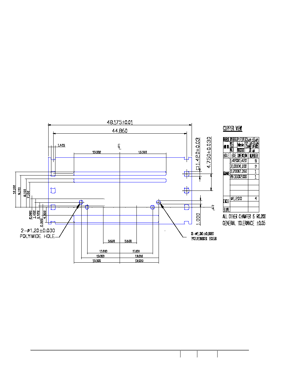
Solomon Systech
Jan 2003
Rev 1.4
SSD1820A/ 21
P 39/43
SSD1820AT TAB PACKAGE DIMENSION (3 OF 3)
DO NOT SCALE THIS DRAWING

SSD1820A/ 21
Rev 1.4
Jan 2003
Solomon Systech
P 40/43
SSD1821T TAB PACKAGE DIMENSION (1 OF 3)
DO NOT SCALE THIS DRAWING
NOTES
1. GENERAL TOLERANCE: ±0.050MM
2. ALL CHAMFER IS R0.20
3. MATERIAL
PI: UPILEX-S 75um+6 THICKNESS
ADHESIVE: TORAY #7100 12 ± 2um THICKNESS
CU: FQ-VLP 25um ± 5um
FLEX COATING: FS-100L
SOLDER RESIST: AR-7100 26 ± 14um
GENERAL TOLERANCE ± 0.300mm
4. PLATING SN: 0.35 ± 0.05um (0.2 ± 0.05um PURE TIN)
5. OPTIONAL FEATURE FOR SSL EXTERNAL USE ONLY WHICH MAY BE REPLACED BY
ÿ2.0MM HOLE
6.
4 SPROCKET HOLES (19.00mm) FOR 1 TAPE

Solomon Systech
Jan 2003
Rev 1.4
SSD1820A/ 21
P 41/43
SSD1821T TAB PACKAGE DIMENSION (2 OF 3)
DO NOT SCALE THIS DRAWING

SSD1820A/ 21
Rev 1.4
Jan 2003
Solomon Systech
P 42/43
SSD1821T TAB PACKAGE DIMENSION (3 OF 3)
DO NOT SCALE THIS DRAWING

Solomon Systech reserves the right to make changes without further notice to any products herein. Solomon Systech makes no warranty, representation or guar-
antee regarding the suitability of its products for any particular purpose, nor does Solomon Systech assume any liability arisin g out of the application or use of
any product or circuit, and specifically disclaims any and all liability, including without limitation consequential or incident al damages. "Typical" parameters can
and do vary in different applications. All operating parameters, including "Typicals" must be validated for each customer application by customer's technical
experts. Solomon Systech does not convey any license under its patent rights nor the rights of others. Solomon Systech products are not designed, intended, or
authorized for use as components in systems intended for surgical implant into the body, or other applications intended to support or sustain life, or for any other
application in which the failure of the Solomon Systech product could create a situation where personal injury or death may occur. Should Buyer purchase or use
Solomon Systech products for any such unintended or unauthorized application, Buyer shall indemnify and hold Solomon Systech and its offices, employees,
subsidiaries, affiliates, and distributors harmless against all claims, costs, damages, and expenses, and reasonable attorney fees arising out of, directly or indi-
rectly, any claim of personal injury or death associated with such unintended or unauthorized use, even if such claim alleges th at Solomon Systech was negligent
regarding the design or manufacture of the part.
Solomon Systech
Jan 2003
Rev 1.4
SSD1820A/ 21
P 43/43
http://www.solomon-systech.com