
i
TABLE OF CONTENTS
1
GENERAL DESCRIPTION................................................................................................................. 1
2
FEATURES ........................................................................................................................................ 2
3
ORDERING INFORMATION.............................................................................................................. 2
4
BLOCK DIAGRAM............................................................................................................................. 3
5
DIE ARRANGEMENT ........................................................................................................................ 4
6
PIN DESCRIPTION ............................................................................................................................ 8
7
FUNCTIONAL BLOCK DESCRIPTIONS ........................................................................................ 11
8
COMMAND DESCRIPTIONS .......................................................................................................... 26
9
MAXIMUM RATINGS ....................................................................................................................... 31
10
DC CHARACTERISTICS ................................................................................................................. 32
11
AC CHARACTERISTICS ................................................................................................................. 34
12
APPLICATION CIRCUIT.................................................................................................................. 38
13
APPENDIXA..................................................................................................................................... 41

ii
TABLE OF FIGURES
Figure 1 - Block Diagram .............................................................................................................................. 3
Figure 2 - SSD1854Z Pin Assignment .......................................................................................................... 4
Figure 3 - Display Data Read with the insertion of Dummy Read .............................................................. 11
Figure 4 - Oscillator Circuitry....................................................................................................................... 12
Figure 5 - SSD1854 Graphic Display Data RAM (GDDRAM) Address Map .............................................. 16
Figure 6 - Contrast Control Voltage Range Curve (TC=-0.1%/
o
C; V
DD
=2.7V; V
CI
=2.7V) ........................... 27
Figure 7 - Contrast Control Flow Set Segment Re-map ............................................................................. 28
Figure 8 - Oscillation Frequency at different VDD at 25
�C ......................................................................... 34
Figure 9 - Parallel 6800-series Interface Timing Characteristics (PS0 = H, PS1 = H) ............................... 35
Figure 10 - Parallel 8080-series Interface Timing Characteristics (PS0 = H, PS1 = L) .............................. 36
Figure 11- Serial Timing Characteristics (PS0 = L) .................................................................................... 37
Figure 12 - LCD Pins Connection of SSD1854Z......................................................................................... 38
Figure 13 - SSD1854U COF Drawing 1...................................................................................................... 41
Figure 14 - SSD1854U COF Drawing 2...................................................................................................... 42
LIST OF TABLE
Table 1 - Ordering Information ...................................................................................................................... 2
Table 2 - SSD1854 Series Die Pad Coordinates .......................................................................................... 5
Table 3 - PS0-2 Interface .............................................................................................................................. 8
Table 4 - Modes of Operation ..................................................................................................................... 12
Table 5 - Command Table .......................................................................................................................... 22
Table 6 - Read Status Byte ......................................................................................................................... 25
Table 7 - Address Increment Table............................................................................................................. 25
Table 8 - Commands Required for R/W (WR#) Actions on RAM ............................................................... 25
Table 9 - Maximum Ratings ........................................................................................................................ 31
Table 10 - DC Characteristics..................................................................................................................... 32
Table 11 - AC Characteristics ..................................................................................................................... 34
Table 12 - Parallel Timing Characteristics 1 ............................................................................................... 35
Table 13 - Parallel Timing Characteristics 2 ............................................................................................... 36
Table 14 - Serial Timing Characteristics ..................................................................................................... 37

SOLOMON SYSTECH
SEMICONDUCTOR TECHNICAL DATA
This document contains information on a new product under definition stage. Solomon Systech Limited reserves
the right to change or discontinue this product without notice.
http://www.solomon-systech.com
SSD1854
Rev 1.0
P 1/43
Aug 2002
Copyright
2003 Solomon Systech Limited
SSD1854
Advance Information
LCD Segment / Common Driver with Controller
CMOS
1 General
Description
SSD1854 is a single-chip CMOS 4 gray scale LCD driver with controller for liquid crystal dot-matrix
graphic display system. It consists of 288 high voltage driving output pins for driving maximum 128
Segments and 160 Commons, customized for 2-sides COF modules.
SSD1854 displays data directly from its internal 128x176x2 bits Graphic Display Data RAM
(GDDRAM). Data/Commands are sent from general MCU through a hardware selectable 6800-/8080-
series compatible Parallel Interface or 3/4 wires Serial Peripheral Interface
.
SSD1854 designed with multi-line-addressing (MLA) scheme to improve the display quality and
reduce the system power consumption.
SSD1854 embeds a DC-DC Converter, a LCD Voltage Regulator, an On-Chip Bias Divider and an
On-Chip oscillator, which reduce the number of external components. With the special design on
minimizing power consumption and die/package layout, SSD1854 is suitable for any portable battery-
driven applications requiring a long operation period and a compact size.
Solomon Systech
Aug 2002
P 2/43
Rev 1.0
SSD1854
2 FEATURES
� 128 x 160 4 gray-levels Graphic Display
� Programmable Multiplex ratio (partial display) [16Mux - 160Mux]
� Single Supply Operation, 1.8 V - 3.3V
� Low Current Sleep Mode (<1.0uA)
� On-Chip Voltage Generator / Regulator & Bias Dividers
� Software selectable 3X / 4X / 5X On-Chip DC-DC Converter
� On-Chip Oscillator
� Maximum +17.0V LCD Driving Output Voltage
� Hardware pin selectable for 8/16-bit 6800-series Parallel Interface, 8/16-bit 8080-series
Parallel Interface, 3-wire Serial Peripheral Interface or 4-wire Serial Peripheral Interface
� Software Selectable On-Chip Bias Dividers
� On-Chip 128 x 176 x 2 Graphic Display Data RAM
� Re-mapping of Row and Column Drivers
� Programmable Window with Vertical Scrolling
� Display Offset Control
� 64 Levels Internal Contrast Control
� Maximum 17MHz SPI or 6MHz PPI operation
� Selectable LCD Driving Voltage Temperature Coefficients (4 settings) [-0.10%/
o
C (POR)]
3 ORDERING
INFORMATION
Table 1 - Ordering Information
Ordering Part Number
Seg
Com
Package Form
SSD1854Z
128
160
Gold Bump Die
SSD1854U
128
160
Die on COF

SSD1854
Rev 1.0
P 3/43
Aug 2002
Solomon Systech
4 BLOCK
DIAGRAM
Figure 1 - Block Diagram
OSC1
RES# PS0-2 CS# DC RW/ E
(WR#) (RD#)
COM0 to
COM159
HV Buffer Cell Level Shifter
Level Selector
288 Bit Latch
Display Timing
Generator
Oscillator
GDDRAM
128 X 160 X 2 Bits
Command Decoder
Command Interface
Parallel / Serial Interface
LCD Driving
Voltage Generator
3X / 4X / 5X
DC/DC Converter,
Voltage Regulator,
Bias Divider,
Contrast Control,
Temperature
Compensation
SEG0~SEG127
VL7
VL6
VL5
VL4
VL3
VL2
VSS
VSS
VDD
DVDD
AVDD
D
8-15
D
7
D
6
D
5
D
4
D
3
D
2
D
1
D
0
(SDA) (SCK)
VCC
C1P
C2P
C3P
C4P
C1N
C2N
REF
VCI
VEXT
CAP
CAN
CBP
CBN
CCP
CCN
CDP
CDN

Solomon Systech
Aug 2002
P 4/43
Rev 1.0
SSD1854
5 DIE
Arrangement
Figure 2 � SSD1854Z Pin Assignment
Note:
1. Diagram showing the die face up.
2. Coordinates are reference to center
of the chip.
3. Unit of coordinates and Size of all
alignment marks are in um.
4. All alignment keys do not contain
gold bump.
Pad1
Pad126
Pad171
Pad324
y
S
i
ze:
94
�
�
�
�
94 um
2
Cent
re:
-
4455,
-
928
x
COM67
COM66
COM65
COM64
COM63
COM62
COM61
COM60
:
:
:
:
:
:
:
:
:
:
COM2
COM1
COM0
SEG0
SEG1
SEG2
SEG3
SEG4
:
:
:
:
:
:
:
:
:
:
:
:
:
:
:
:
:
:
:
:
:
:
:
:
:
SEG78
SEG79
SEG80
SEG81
SEG82
SEG83
SEG84
SEG85
COM110
COM111
COM112
COM113
COM114
:
:
:
:
:
:
:
:
:
:
:
:
:
:
:
:
:
:
:
:
COM155
COM156
COM157
COM158
COM159
VSS
VSS
N/C
CDN
CDP
CCN
CCP
CBN
CBP
CAN
CAP
VL7
VL6
VL5
VL4
VL3
VL2
VSS
VSS
N/C
VDD
VEXT
REF
AVSS
DVSS
VSS
C4P
C2N
C2P
C1P
C1N
C3P
VCC
VSS
VSS
VCI
AVDD
DVDD
D15
D14
D13
D12
D11
D10
D9
D8
D7(SDA)
D6(SCK)
D5
D4
D3
D2
D1
D0
VDD
E(RD#)
R/W(WR#)
VSS
D/C
RES#
VDD
CS#
N/C
VSS
PS1
VDD
VSS
PS2
PS0
N/C
OSC1
VDD
N/C
N/C
N/C
N/C
N/C
C
O
M
68
C
O
M
69
C
O
M
70
C
O
M
71
:
:
:
:
:
C
O
M
106
C
O
M
107
C
O
M
108
C
O
M
109
N/C
N/C
SEG
8
6
SEG
8
7
SEG
8
8
SEG
8
9
:
:
:
:
:
:
SE
G124
SE
G125
SE
G126
SE
G127
N/C
S
i
ze:
94
�
�
�
�
94 um
2
Cent
re:
4796,
-
928
S
i
ze:
70
�
�
�
�
70 um
2
Cent
re:
1986,
676
Size:
116
�
�
�
�
116 um
2
Cent
re:
3005,
673
X Y
Unit
Chip Size
10.72 2.77
mm
Chip
Thickness
723.9
� 25
�m
Pad #
X
Y
1 � 4
43 � 51
59 � 75
77 � 126
171 � 324
40 70
5 � 42
52 � 58
76
50 60
Bump Size
127 � 170
325 � 368
70 40
�m
Bump
Height
18 (Typ.)
�m
SSD1854
Rev 1.0
P 5/43
Aug 2002
Solomon Systech
Table 2 - SSD1854 Series Die Pad Coordinates
Pad
#
Pad
Name
X-pos Y-pos
Pad
#
Pad
Name
X-pos Y-pos
Pad
#
Pad
Name
X-pos Y-pos
1
N/C -4520.2 -1239.7 51 VSS -287.1 -1239.7 101 COM135 3223.1 -1214.3
2
N/C -4451.6 -1239.7 52 DVSS -206.0 -1243.7 102 COM134 3282.5 -1214.3
3
N/C -4383.0 -1239.7 53 AVSS -106.7 -1243.7 103 COM133 3341.9 -1214.3
4
N/C -4314.4 -1239.7 54 REF
-7.5 -1243.7 104 COM132 3401.3 -1214.3
5
VDD -4233.3 -1243.7 55 VEXT 81.6 -1243.7 105 COM131 3460.7 -1214.3
6
OSC1 -4144.2 -1243.7 56 VDD 170.7 -1243.7 106 COM130 3520.1 -1214.3
7
N/C -4055.1 -1243.7 57
N/C
259.8 -1243.7 107 COM129 3579.5 -1214.3
8
PS0 -3966.0 -1243.7 58 VSS 348.9 -1243.7 108 COM128 3638.9 -1214.3
9
PS2 -3876.9 -1243.7 59 VSS 430.0 -1239.7 109 COM127 3698.3 -1214.3
10
VSS -3787.8 -1243.7 60
VL2
499.4 -1239.7 110 COM126 3757.7 -1214.3
11
VDD -3698.7 -1243.7 61
VL3
568.0 -1239.7 111 COM125 3817.1 -1214.3
12
PS1 -3609.6 -1243.7 62
VL4
636.6 -1239.7 112 COM124 3876.5 -1214.3
13
VSS -3520.5 -1243.7 63
VL5
705.2 -1239.7 113 COM123 3935.9 -1214.3
14
N/C -3431.4 -1243.7 64
VL6
773.8 -1239.7 114 COM122 3995.3 -1214.3
15
CS
-3342.3 -1243.7 65
VL7
868.4 -1239.7 115 COM121 4054.7 -1214.3
16
VDD -3253.2 -1243.7 66 CAP 963.0 -1239.7 116 COM120 4114.1 -1214.3
17
RES
-3164.1 -1243.7 67 CAN 1031.6 -1239.7 117 COM119 4173.5 -1214.3
18
D/ C
-3075.0 -1243.7 68 CBP 1100.3 -1239.7 118 COM118 4232.9 -1214.3
19
VSS -2985.9 -1243.7 69 CBN 1168.8 -1239.7 119 COM117 4292.3 -1214.3
20
R/
W
( WR )
-2896.8 -1243.7 70 CCP 1237.4 -1239.7 120 COM116 4351.7 -1214.3
21
E( RD )
-2807.7 -1243.7 71 CCN 1306.0 -1239.7 121 COM115 4411.1 -1214.3
22
VDD -2718.6 -1243.7 72 CDP 1374.6 -1239.7 122 COM114 4470.5 -1214.3
23
D0
-2629.5 -1243.7 73 CDN 1443.2 -1239.7 123 COM113 4529.9 -1214.3
24
D1
-2540.4 -1243.7 74
N/C 1511.8 -1239.7 124 COM112 4589.3 -1214.3
25
D2
-2451.3 -1243.7 75 VSS 1580.4 -1239.7 125 COM111 4648.7 -1214.3
26
D3
-2362.2 -1243.7 76 VSS 1661.5 -1243.7 126 COM110 4708.1 -1214.3
27
D4
-2273.1 -1243.7 77 COM159 1797.5 -1214.3 127
N/C
5192.1 -1277.1
28
D5
-2184.0 -1243.7 78 COM158 1856.9 -1214.3 128 COM109 5192.1 -1217.7
29 D6
(SCK) -2094.9 -1243.7 79 COM157 1916.3 -1214.3 129 COM108 5192.1 -1158.3
30 D7
(SDA) -2005.8 -1243.7 80 COM156 1975.7 -1214.3 130 COM107 5192.1 -1098.9
31
D8
-1916.7 -1243.7 81 COM155 2035.1 -1214.3 131 COM106 5192.1 -1039.5
32
D9
-1827.6 -1243.7 82 COM154 2094.5 -1214.3 132 COM105 5192.1 -980.1
33
D10 -1738.5 -1243.7 83 COM153 2153.9 -1214.3 133 COM104 5192.1 -920.7
34
D11 -1649.4 -1243.7 84 COM152 2213.3 -1214.3 134 COM103 5192.1 -861.3
35
D12 -1560.3 -1243.7 85 COM151 2272.7 -1214.3 135 COM102 5192.1 -801.9
36
D13 -1471.2 -1243.7 86 COM150 2332.1 -1214.3 136 COM101 5192.1 -742.5
37
D14 -1382.1 -1243.7 87 COM149 2391.5 -1214.3 137 COM100 5192.1 -683.1
38
D15 -1293.0 -1243.7 88 COM147 2450.9 -1214.3 138 COM99 5192.1 -623.7
39 DVDD -1203.9 -1243.7 89 COM147 2510.3 -1214.3 139 COM98 5192.1 -564.3
40
AVDD -1104.7 -1243.7 90 COM146 2569.7 -1214.3 140 COM97 5192.1 -504.9
41
VCI -1005.5 -1243.7 91 COM145 2629.1 -1214.3 141 COM96 5192.1 -445.5
42
VSS
-916.4 -1243.7 92 COM144 2688.5 -1214.3 142 COM95 5192.1 -386.1
43
VSS
-835.9 -1239.7 93 COM143 2747.9 -1214.3 143 COM94 5192.1 -326.7
44
VCC
-767.3 -1239.7 94 COM142 2807.3 -1214.3 144 COM93 5192.1 -267.3
45
C3P
-698.7 -1239.7 95 COM141 2866.7 -1214.3 145 COM92 5192.1 -207.9
46
C1N
-630.1 -1239.7 96 COM140 2926.1 -1214.3 146 COM91 5192.1 -148.5
47
C1P
-561.5 -1239.7 97 COM139 2985.5 -1214.3 147 COM90 5192.1 -89.1
48
C2P
-492.9 -1239.7 98 COM138 3044.9 -1214.3 148 COM89 5192.1 -29.7
49
C2N
-424.3 -1239.7 99 COM137 3104.3 -1214.3 149 COM88 5192.1 29.7
50
C4P
-355.7 -1239.7 100 COM136 3163.7 -1214.3 150 COM87 5192.1 89.1

Solomon Systech
Aug 2002
P 6/43
Rev 1.0
SSD1854
Pad
#
Pad
Name
X-pos Y-pos
Pad
#
Pad
Name
X-pos Y-pos
Pad
#
Pad
Name
X-pos Y-pos
151 COM86 5192.1 148.5 201 COM37 2926.1 1214.3 251 SEG12 -162.7 1214.3
152 COM85 5192.1 207.9 202 COM36 2866.7 1214.3 252 SEG13 -222.1 1214.3
153 COM84 5192.1 267.3 203 COM35 2807.3 1214.3 253 SEG14 -281.5 1214.3
154 COM83 5192.1 326.7 204 COM34 2747.9 1214.3 254 SEG15 -340.9 1214.3
155 COM82 5192.1 386.1 205 COM33 2688.5 1214.3 255 SEG16 -400.3 1214.3
156 COM81 5192.1 445.5 206 COM32 2629.1 1214.3 256 SEG17 -459.7 1214.3
157 COM80 5192.1 504.9 207 COM31 2569.7 1214.3 257 SEG18 -519.1 1214.3
158 COM79 5192.1 564.3 208 COM30 2510.3 1214.3 258 SEG19 -578.5 1214.3
159 COM78 5192.1 623.7 209 COM29 2450.9 1214.3 259 SEG20 -637.9 1214.3
160 COM77 5192.1 683.1 210 COM28 2391.5 1214.3 260 SEG21 -697.3 1214.3
161 COM76 5192.1 742.5 211 COM27 2332.1 1214.3 261 SEG22 -756.7 1214.3
162 COM75 5192.1 801.9 212 COM26 2272.7 1214.3 262 SEG23 -816.1 1214.3
163 COM74 5192.1 861.3 213 COM25 2213.3 1214.3 263 SEG24 -875.5 1214.3
164 COM73 5192.1 920.7 214 COM24 2153.9 1214.3 264 SEG25 -934.9 1214.3
165 COM72 5192.1 980.1 215 COM23 2094.5 1214.3 265 SEG26 -994.3 1214.3
166 COM71 5192.1 1039.5 216 COM22 2035.1 1214.3 266 SEG27
-1053.7
1214.3
167 COM70 5192.1 1098.9 217 COM21 1975.7 1214.3 267 SEG28
-1113.1
1214.3
168 COM69 5192.1 1158.3 218 COM20 1916.3 1214.3 268 SEG29
-1172.5
1214.3
169 COM68 5192.1 1217.7 219 COM19 1856.9 1214.3 269 SEG30
-1231.9
1214.3
170 N/C 5192.1
1277.1
220
COM18
1797.5
1214.3
270
SEG31
-1291.3
1214.3
171 COM67 4708.1 1214.3 221 COM17 1738.1 1214.3 271 SEG32
-1350.7
1214.3
172 COM66 4648.7 1214.3 222 COM16 1678.7 1214.3 272 SEG33
-1410.1
1214.3
173 COM65 4589.3 1214.3 223 COM15 1619.3 1214.3 273 SEG34
-1469.5
1214.3
174 COM64 4529.9 1214.3 224 COM14 1559.9 1214.3 274 SEG35
-1528.9
1214.3
175 COM63 4470.5 1214.3 225 COM13 1500.5 1214.3 275 SEG36
-1588.3
1214.3
176 COM62 4411.1 1214.3 226 COM12 1441.1 1214.3 276 SEG37
-1647.7
1214.3
177 COM61 4351.7 1214.3 227 COM11 1381.7 1214.3 277 SEG38
-1707.1
1214.3
178 COM60 4292.3 1214.3 228 COM10 1322.3 1214.3 278 SEG39
-1766.5
1214.3
179 COM59 4232.9 1214.3 229 COM9 1262.9 1214.3 279 SEG40
-1825.9
1214.3
180 COM58 4173.5 1214.3 230 COM8 1203.5 1214.3 280 SEG41
-1885.3
1214.3
181 COM57 4114.1 1214.3 231 COM7 1144.1 1214.3 281 SEG42
-1944.7
1214.3
182 COM56 4054.7 1214.3 232 COM6 1084.7 1214.3 282 SEG43
-2004.1
1214.3
183 COM55 3995.3 1214.3 233 COM5 1025.3 1214.3 283 SEG44
-2063.5
1214.3
184 COM54 3935.9 1214.3 234 COM4 965.9 1214.3 284 SEG45
-2122.9
1214.3
185 COM53 3876.5 1214.3 235 COM3 906.5 1214.3 285 SEG46
-2182.3
1214.3
186 COM52 3817.1 1214.3 236 COM2 847.1 1214.3 286 SEG47
-2241.7
1214.3
187 COM51 3757.7 1214.3 237 COM1 787.7 1214.3 287 SEG48
-2301.1
1214.3
188 COM50 3698.3 1214.3 238 COM0 728.3 1214.3 288 SEG49
-2360.5
1214.3
189 COM49 3638.9 1214.3 239 SEG0 550.1 1214.3 289 SEG50
-2419.9
1214.3
190 COM48 3579.5 1214.3 240 SEG1 490.7 1214.3 290 SEG51
-2479.3
1214.3
191 COM47 3520.1 1214.3 241 SEG2 431.3 1214.3 291 SEG52
-2538.7
1214.3
192 COM46 3460.7 1214.3 242 SEG3 371.9 1214.3 292 SEG53
-2598.1
1214.3
193 COM45 3401.3 1214.3 243 SEG4 312.5 1214.3 293 SEG54
-2657.5
1214.3
194 COM44 3341.9 1214.3 244 SEG5 253.1 1214.3 294 SEG55
-2716.9
1214.3
195 COM43 3282.5 1214.3 245 SEG6 193.7 1214.3 295 SEG56
-2776.3
1214.3
196 COM42 3223.1 1214.3 246 SEG7 134.3 1214.3 296 SEG57
-2835.7
1214.3
197 COM41 3163.7 1214.3 247 SEG8 74.9 1214.3 297 SEG58
-2895.1
1214.3
198 COM40 3104.3 1214.3 248 SEG9 15.5 1214.3 298 SEG59
-2954.5
1214.3
199 COM39 3044.9 1214.3 249 SEG10 -43.9 1214.3 299 SEG60
-3013.9
1214.3
200 COM38 2985.5 1214.3 250 SEG11 -103.3 1214.3 300 SEG61
-3073.3
1214.3

SSD1854
Rev 1.0
P 7/43
Aug 2002
Solomon Systech
Pad
#
Pad
Name
X-pos Y-pos
Pad
#
Pad
Name
X-pos Y-pos
301 SEG62 -3132.7
1214.3 351 SEG111 -5192.1 -267.3
302 SEG63 -3192.1
1214.3 352 SEG112 -5192.1 -326.7
303 SEG64 -3251.5
1214.3 353 SEG113 -5192.1 -386.1
304 SEG65 -3310.9
1214.3 354 SEG114 -5192.1 -445.5
305 SEG66 -3370.3
1214.3 355 SEG115 -5192.1 -504.9
306 SEG67 -3429.7
1214.3 356 SEG116 -5192.1 -564.3
307 SEG68 -3489.1
1214.3 357 SEG117 -5192.1 -623.7
308 SEG69 -3548.5
1214.3 358 SEG118 -5192.1 -683.1
309 SEG70 -3607.9
1214.3 359 SEG119 -5192.1 -742.5
310 SEG71 -3667.3
1214.3 360 SEG120 -5192.1 -801.9
311 SEG72 -3726.7
1214.3 361 SEG121 -5192.1 -861.3
312 SEG73 -3786.1
1214.3 362 SEG122 -5192.1 -920.7
313 SEG74 -3845.5
1214.3 363 SEG123 -5192.1 -980.1
314 SEG75 -3904.9
1214.3 364 SEG124 -5192.1 -1039.5
315 SEG76 -3964.3
1214.3 365 SEG125 -5192.1 -1098.9
316 SEG77 -4023.7
1214.3 366 SEG126 -5192.1 -1158.3
317 SEG78 -4083.1
1214.3 367 SEG127 -5192.1 -1217.7
318 SEG79 -4142.5
1214.3 368 N/C -5192.1 -1277.1
319 SEG80 -4201.9
1214.3
320 SEG81 -4261.3
1214.3
321 SEG82 -4320.7
1214.3
322 SEG83 -4380.1
1214.3
323 SEG84 -4439.5
1214.3
324 SEG85 -4498.9
1214.3
325 N/C -5192.1
1277.1
326 SEG86 -5192.1
1217.7
327 SEG87 -5192.1
1158.3
328 SEG88 -5192.1
1098.9
329 SEG89 -5192.1
1039.5
330 SEG90 -5192.1 980.1
331 SEG91 -5192.1 920.7
332 SEG92 -5192.1 861.3
333 SEG93 -5192.1 801.9
334 SEG94 -5192.1 742.5
335 SEG95 -5192.1 683.1
336 SEG96 -5192.1 623.7
337 SEG97 -5192.1 564.3
338 SEG98 -5192.1 504.9
339 SEG99 -5192.1 445.5
340 SEG100 -5192.1 386.1
341 SEG101 -5192.1 326.7
342 SEG102 -5192.1 267.3
343 SEG103 -5192.1 207.9
344 SEG104 -5192.1 148.5
345 SEG105 -5192.1 89.1
346 SEG106 -5192.1 29.7
347 SEG107 -5192.1 -29.7
348 SEG108 -5192.1 -89.1
349 SEG109 -5192.1 -148.5
350 SEG110 -5192.1 -207.9
Pad #
Diff.
Unit
1 � 4
43 � 51
60 � 64
66 � 75
68.6
4 � 5
51 � 52
58 � 59
75 � 76
81.1
5 � 39
41 � 42
54 � 58
89.1
39 � 41
53 � 54
99.2
42 � 43
80.6
52 � 53
99.3
59 � 60
69.5
64 � 66
94.6
76 � 77
136
77 � 126
127 � 170
171 � 238
239 � 324
325 � 368
59.4
Pad Pitch
238 � 239
178.2
�m
Pad Space
19.4 (min)
�m
Pad126
SSD1854 IC
X
Y
Pad1
Pad171
Pad324
Solomon Systech
Aug 2002
P 8/43
Rev 1.0
SSD1854
6 PIN
DESCRIPTION
6.1
RES
This pin is reset signal input. When the pin is low, initialization of the chip is executed.
6.2 PS0-2
These 3 pins use together to determine the interface protocol between the driver and MCU according
to the following table.
Table 3 - PS0-2 Interface
PS0 PS1 PS2 Interface
L
L
X
3-wire SPI (write only)
L
H
X
4-wire SPI (write only)
H
8080 parallel interface (8-bits read and 16-bits write)
H L
L
8080 parallel interface (8-bits read and 8-bits write)
H
6800 parallel interface (8-bits read and 16-bits write)
H H
L
6800 parallel interface (8-bits read and 8-bits write)
6.3
CS
This pin is chip select input. The chip is enabled for display data/command transfer only when
CS
is
low.
For 6800-series parallel mode, when E pin is pulled high, the read/write cycle is initiated by pulling low
of this
CS
pin.
6.4 D/
C
This input pin is to identify display data/command cycle. When the pin is high, the data written to the
driver will be written into display RAM. When the pin is low, the data will be interpreted as command.
This pin must be connected to V
SS
when 3-lines SPI interface is used.
6.5 R/
W
(
WR
)
This pin is microprocessor interface signal. When interfacing to an 6800-series microprocessor, the
signal indicates read mode when high and write mode when low. When interfacing to an 8080-
microprocessor, a data write operation is initiated when
R/W ( WR )
is low and the chip is selected.
6.6 E(
RD
)
This pin is microprocessor interface signal. When interfacing to an 6800-series microprocessor, a data
operation is initiated when
E( RD )
is high and the chip is selected. When interfacing to an 8080-
microprocessor, a data read operation is initiated when
E( RD )
is low and the chip is selected.
6.7 D
0
-D
15
D
0
-D
7
are bi-directional and D
8
-D
15
are input only data pins to be connected to the microprocessor's
data bus. When serial mode is selected, D
7
is the serial data input SDA and D
6
is the serial clock input
SCK. All unused data pins must be connected to ground.

SSD1854
Rev 1.0
P 9/43
Aug 2002
Solomon Systech
6.8 OSC1
This pin is for oscillator frequency selection. A resistor must be connected between this pin and V
DD
when using the internal oscillator. The suggested value of the resistor is 680K ohm. Please refer to the
Figure 8 for details.
6.9 REF
This pin is an input pin to enable the internal reference voltage used for the internal regulator. When it
is high, an internal reference voltage source will be used. When it is low, and external reference must
be provided in V
EXT
.
6.10 DV
DD
, AV
DD
Digital and Analog power supply pins, must be connected to same external source.
6.11 V
DD
Internally connected to DV
DD
for pull high purpose. Can be connected to DVDD externally or float.
6.12 DV
SS
, AV
SS
Digital and Analog ground, must be connected to external ground.
6.13 V
SS
Internally connected to DV
SS
for pull low purpose.
6.14 V
CI
Reference voltage input for internal DC-DC converter. The voltage of generated V
CC
equals to the
multiple factor (3X, 4X or 5X) times V
CI
with respect to V
SS
.
Note: Voltage at this input pin must be larger than or equal to AV
DD
and DV
DD.
6.15 V
CC
Voltage at this pin must be greater then V
L4
+ 2V. It can be supplied externally or generated by the
internal DC-DC converter.
When using internal DC-DC converter as generator, voltage at this pin is for internal reference only. It
CANNOT be used for driving external circuitries.
6.16 C
1P
,
C
1N
,
C
3P
, C
2P
,
C
2N
, and C
4P
When internal DC-DC voltage converter is used, external capacitor(s) is/are connected among these
pins.
6.17 V
L7
This pin is the most positive LCD driving voltage. It can be generated by the internal regulator or
supply externally when internal regulator and divider are turned off.
6.18 V
EXT
This pin is an input to provide an external voltage reference for the internal voltage regulator when
REF pin is pulled low.
6.19 V
L7
,
V
L6
,
V
L5
,
V
L4
,
V
L3
and V
L2
LCD driving voltages. They can be supplied externally or generated by the internal regulator and
divider or supplied externally when regulator and divider are turned off. They have the following
relationship:
V
L7
> V
L6
> V
L5
> V
L4
> V
L3
> V
L2
> V
SS

Solomon Systech
Aug 2002
P 10/43 Rev 1.0
SSD1854
6.20 COM0 � COM159
These pins provide the row driving signal COM0 � COM159 to the LCD panel.
6.21 SEG0 � SEG127
These pins provide the LCD column driving signal. Their voltage level is V
SS
during sleep mode.
6.22 C
AP
,
C
AN
,
C
BP
, C
BN
, C
CP
, C
CN
,
C
DP
, and C
DN
These pins are connected to four capacitors when internal divider is enabled.
6.23 N/C
These No Connection pins should NOT be connected to any signals nor shorted together. These N/C
pins should be left open.
SSD1854
Rev 1.0
P 11/43 Aug 2002
Solomon Systech
7 FUNCTIONAL BLOCK DESCRIPTIONS
7.1 Command Decoder and Command Interface
This module determines whether the input data is interpreted as data or command. Data is
directed to this module based upon the input of the
D/ C
pin. If
D/ C
is high, data is written to
Graphic Display Data RAM (GDDRAM). If
D/ C
is low, the input at D
0
-D
15
is interpreted as a
Command and it will be decoded and written to the corresponding command register.
Reset is of the same function as Power ON Reset (POR). Once
RES
receives a negative reset
pulse of about 1us, all internal circuitry will be back to its initial status. Refer to Command
Description section for more information.
7.2 MPU Parallel 6800-series Interface
The parallel interface consists of 8/16 data pins (D
0
- D
15
),
R/W( WR )
,
D/ C
,
E( RD )
and
CS
.
R/ W ( WR )
input High indicates a read operation from the Graphic Display Data RAM
(GDDRAM) or the status register.
R/W( WR )
input Low indicates a write operation to Display
Data RAM or Internal Command Registers depending on the status of
D/ C
input. The
E( RD )
and
CS
input serves as data latch signal (clock) when they are high and low respectively. Refer
to Figure 9 of parallel timing characteristics for Parallel Interface Timing Diagram of 6800-series
microprocessors.
In order to match the operating frequency of display RAM with that of the microprocessor, some
pipeline processing is internally performed which requires the insertion of a dummy read before
the first actual display data read. This is shown in Figure 3 below.
Figure 3 � Display Data Read with the insertion of Dummy Read
7.3 MPU Parallel 8080-series Interface
The parallel interface consists of 8/16 data pins (D
0
-D
15
),
R/W( WR )
,
E( RD )
,
D/ C
and
CS
. The
CS
input serves as data latch signal (clock) when it is low. Whether it is display data or status
register read is controlled by
D/ C
.
R/W( WR )
and
E( RD )
input indicates a write or read cycle
when
CS
is low. Refer to Figure 10 of parallel timing characteristics for Parallel Interface Timing
Diagram of 8080-series microprocessor.
Similar to 6800-series interface, a dummy read is also required before the first actual display
data read.
R/W(WR)
E(RD)
N
n
n+1
n+2
data bus
write column address
dummy read
data read1
data read 2
data read 3

Solomon Systech
Aug 2002
P 12/43 Rev 1.0
SSD1854
OSC1
Oscillator
enable
Internal Resistor
OSCE
Buffer
enable
Oscillation Circuit
enable
(CL)
7.4 MPU Serial 4-wire Interface
The serial interface consists of serial clock SCK, serial data SDA,
D/ C
and
CS
. SDA is shifted
into an 8-bit shift register on every rising edge of SCL in the order of D
7
, D
6
, ... D
0
.
D/ C
is
sampled on every eighth clock and the data byte in the shift register is written to the Display
Data RAM or command register in the same clock. No extra clock or command is required to
end the transmission.
7.5 MPU Serial 3-wire interface
Operation is similar to 4-wire serial interface while
D/ C
is not been used. The Display Data
Length instruction is used to indicate that a specified number display data byte(s) (1-256) are to
be transmitted. Next byte after the display data string is handled as a command.
It should be noted that if there is a signal glitch at SCK that causing an out of synchronization in
the serial communication, a hardware reset pulse at
RES
pin is required to initialize the chip for
re-synchronization.
Table 4 -Modes of Operation
6800 Parallel
8080 Parallel
Serial
Data Read
8-bitys
8-bits
No
Data
Write
8/16-bits 8/16-bits 8-bits
Command Read Status only
Status only
No
Command
Write
Yes Yes Yes
7.6 Graphic Display Data RAM (GDDRAM)
The GDDRAM is a bit mapped static RAM holding the bit pattern to be displayed. The size of
the RAM is 128 x 176 x 2 = 45,056bits.
Figure 5 is a description of the GDDRAM address map. For mechanical flexibility, re-mapping
on both Segment and Common outputs are provided. For vertical scrolling of display, an internal
register storing the display start line can be set to control the portion of the RAM data to be
mapped to the display.
Figure 5 shows the case in which the display start line register is set at 30H. For those
GDDRAM out of the display common range, they could still be accessed, for either preparation
of vertical scrolling data or even for the system usage.
7.7 Oscillator
Circuit
This module is an On-Chip low power RC oscillator circuitry (Figure 4). The oscillator generates
the clock for the DC-DC voltage converter. This clock is also used in the Display Timing
Generator.
Figure 4 - Oscillator Circuitry

SSD1854
Rev 1.0
P 13/43 Aug 2002
Solomon Systech
7.8 LCD Driving Voltage Generator and Regulator
This module generates the LCD voltage needed for display output. It takes a single supply input
and generates necessary bias voltages.
It consists of:
1.
3X, 4X and 5X DC-DC voltage converter:
The booster output at V
CC
equals to n time VCI where n is the booster ration. The VCC
voltage must be greater than 2V + VL4 or 2V + � VL7. Please refer to application notes
for details.
2. Voltage
Regulator
Feedback gain control for initial LCD voltage. Internal resistors are connected between
V
SS
and V
R
(internal contrast voltage reference), and between V
R
and V
L7
. These
resistors are chosen to give the desired V
L7
according to the following equation:
con
L
V
R
R
V
�
+
=
1
2
1
7
and
(
)
ref
con
V
V
�
-
-
=
210
63
1
where:
V
ref
is the internally generated reference voltage
(1+R2/R1) is the software programmable IRS value
is the software contrast level from 0 to 63
3.
Bias Divider
There is an on-chip bias divider inside the chip selected by software which generate all
V
L2
~V
L7
levels automatically.
4. Contrast
Control
Software control of 64 voltage levels of LCD voltage.
5.
Bias Ratio Selection circuitry
Software control of different bias ratios to match the characteristic of LCD panel.
6.
Self adjust temperature compensation circuitry
Provide 4 different compensation grade selections to satisfy the various liquid crystal
temperature grades. The grading can be selected by software control. Defaulted
temperature coefficient (TC) value is -0.1%/�C.
7.9 288 Bit Latch
A register carries the display signal information. In 128 X 160 display-mode, data will be fed to
the HV-buffer Cell and level-shifted to the required level.
7.10 Level selector
Level Selector is a control of the display synchronization. Display voltage can be separated into
two sets and used with different cycles. Synchronization is important since it selects the
required LCD voltage level to the HV Buffer Cell, which in turn outputs the COM or SEG LCD
waveform.
7.11 HV Buffer Cell (Level Shifter)
HV Buffer Cell works as a level shifter which translated the low voltage output signal to the
required driving voltage. The output is shifted out with an internal FRM clock, which comes
from the Display Timing Generator. The voltage levels are given by the level selector, which is
synchronized with the internal M signal.
For a panel with N rows and M columns, the optimal LCD driving voltage are given as:

Solomon Systech
Aug 2002
P 14/43 Rev 1.0
SSD1854
(
)
th
SS
L
L
L
V
N
N
N
V
V
V
V
�
-
�
=
-
=
-
1
2
4
4
4
7
(
)
N
V
V
V
V
V
V
L
L
L
L
L
L
4
7
2
4
4
6
4
-
�
=
-
=
-
And
2
4
6
3
4
4
5
L
L
L
L
L
L
V
V
V
V
V
V
-
=
-
=
-
where:
V
th
is the threshold voltage of the LCD panel
V
L7
is the maximum (Row) driving level with reference to V
SS
(The peak-to-peak Row driving voltage is given by V
L7
-V
SS
)
V
L4
is the middle of all driving levels
V
L6
, V
L5
, V
L3
and V
L2
are the other Column driving levels
(The peak-to-peak Column driving voltage is given by V
L6
-V
SS
)
Relationship between the levels:
V
L7
> V
L6
> V
L5
> V
L4
> V
L3
> V
L2
> V
SS
and
V
CC
> V
L4
+ 2V
SSD1854
Rev 1.0
P 15/43 Aug 2002
Solomon Systech
7.12 Default Setting after Reset
When
RES
input is low, the chip is initialized to the following:
Register Default
Value
Descriptions
Page address
0
Column address
0
Display ON/OFF
0
Display OFF
Display Start Line
0
GDDRAM page 0,D0
Display Offset
0
COM0 is mapped to ROW0
Mux Ratio
A0H
160 Mux
Normal/Reverse Display
0
Normal Display
N-line Inversion
0
No N-line Inversion
Entire Display
0
Entire Display is OFF
Power Control
0,0,0
Booster, regulator & divider are both disabled
DC-DC booster
0
3X booster is selected
Internal Resistor Ratio
0
Gain = 3.2 (IR0)
Contrast 20H
Middle
LCD Bias Ratio
6
Optimized for 160 Mux
Scan direction of COM
0
Normal Scan direction
Segment Re-map
0
Segment re-map is disabled
Internal oscillator
0
Internal oscillator is OFF
Power save mode
0
Power save mode is OFF
Data display length
0
FRC, PWM Mode
0
4FRC, 9PWM
White Palette
(0, 0, 0, 0)
Light Gray Palette
(0, 0, 0, 0)
Dark Gray Palette
(9, 9, 9, 9)
Black Palette
(9, 9, 9, 9)
Test mode
0
Test mode is OFF
Temperature coefficient
2
TC2 (-0.1%/
o
C)
Upper window corner
0,0
Lower window corner
127,159
When RESET command is issued, the following parameters are initialized only:
Register Default
Value
Descriptions
Page address
0
Column address
0
Display Start Line
0
GDDRAM page 0,D0
Internal Resistor Ratio
0
Gain = 3.2 (IR0)
Contrast 20H
Data display length
0
FRC, PWM Mode
0
4FRC, 9PWM
White Palette
(0, 0, 0, 0)
Light Gray Palette
(0, 0, 0, 0)
Dark Gray Palette
(9, 9, 9, 9)
Black Palette
(9, 9, 9, 9)
Solomon Systech
Aug 2002
P 16/43 Rev 1.0
SSD1854
Figure 5 - SSD1854 Graphic Display Data RAM (GDDRAM) Address Map
Seg Normal
� � � � � �
Seg Remapped
� � � � � �
� � � � � �
00h
D0 (LSB)
� � � � � �
0
159 156
3
0
159
0
159
5
154
01h
D1
� � � � � �
1
158 157
2
1
158
1
158
6
153
02h
D2
� � � � � �
2
157 158
1
2
157
2
157
7
152
03h
D3
� � � � � �
3
156 159
0
3
156
3
156
8
151
04h
D4
� � � � � �
4
155
-
-
4
155
4
155
9
150
05h
D5
� � � � � �
5
154
-
-
5
154
5
154
10
149
06h
D6
� � � � � �
6
153
-
-
136
23
-
-
-
-
07h
D7 (MSB)
� � � � � �
7
152
-
-
137
22
-
-
-
-
08h
D0 (LSB)
� � � � � �
8
151
-
-
138
21
-
-
-
-
09h
D1
� � � � � �
9
150
-
-
139
20
-
-
-
-
0Ah
D2
� � � � � �
10
149
-
-
-
-
-
-
-
-
0Bh
D3
� � � � � �
11
148
-
-
-
-
6
153
11
148
0Ch
D4
� � � � � �
12
147
-
-
-
-
7
152
12
147
0Dh
D5
� � � � � �
13
146
-
-
-
-
8
151
13
146
0Eh
D6
� � � � � �
14
145
-
-
-
-
9
150
14
145
0Fh
D7 (MSB)
� � � � � �
15
144
-
-
-
-
10
149
15
144
10h
D0 (LSB)
� � � � � �
16
143
-
-
-
-
11
148
16
143
11h
D1
� � � � � �
17
142
-
-
-
-
12
147
17
142
12h
D2
� � � � � �
18
141
-
-
-
-
13
146
18
141
13h
D3
� � � � � �
19
140
-
-
-
-
14
145
19
140
14h
D4
� � � � � �
20
139
0
159
-
-
15
144
20
139
15h
D5
� � � � � �
21
138
1
158
-
-
16
143
21
138
16h
D6
� � � � � �
22
137
2
157
-
-
17
142
22
137
17h
D7 (MSB)
� � � � � �
23
136
3
156
-
-
18
141
23
136
18h
D0 (LSB)
� � � � � �
24
135
4
155
-
-
19
140
24
135
19h
D1
� � � � � �
25
134
5
154
-
-
20
139
25
134
1Ah
D2
� � � � � �
26
133
6
153
6
153
21
138
26
133
1Bh
D3
� � � � � �
27
132
7
152
7
152
22
137
27
132
1Ch
D4
� � � � � �
28
131
8
151
8
151
23
136
28
131
1Dh
D5
� � � � � �
29
130
9
150
9
150
24
135
29
130
1Eh
D6
� � � � � �
30
129
10
149
10
149
25
134
30
129
1Fh
D7 (MSB)
� � � � � �
31
128
11
148
11
148
26
133
31
128
� � �
�
� � �
�
� � �
�
� � �
�
� � �
�
� � �
�
� � �
�
� � �
�
� � �
�
� � �
�
� � �
�
� � �
�
� � �
�
80h
D0 (LSB)
� � � � � �
128
31
108
51
108
51
123
36
127
32
81h
D1
� � � � � �
129
30
109
50
109
50
124
35
128
31
82h
D2
� � � � � �
130
29
110
49
110
49
125
34
129
30
83h
D3
� � � � � �
131
28
111
48
111
48
126
33
130
29
84h
D4
� � � � � �
132
27
112
47
112
47
127
32
131
28
85h
D5
� � � � � �
133
26
113
46
113
46
128
31
132
27
86h
D6
� � � � � �
134
25
114
45
114
45
129
30
133
26
87h
D7 (MSB)
� � � � � �
135
24
115
44
115
44
130
29
134
25
88h
D0 (LSB)
� � � � � �
136
23
116
43
116
43
131
28
135
24
89h
D1
� � � � � �
137
22
117
42
117
42
132
27
136
23
8Ah
D2
� � � � � �
138
21
118
41
118
41
133
26
137
22
8Bh
D3
� � � � � �
139
20
119
40
119
40
134
25
138
21
8Ch
D4
� � � � � �
140
19
120
39
140
19
140
19
145
14
8Dh
D5
� � � � � �
141
18
121
38
141
18
141
18
146
13
8Eh
D6
� � � � � �
142
17
122
37
142
17
142
17
147
12
8Fh
D7 (MSB)
� � � � � �
143
16
123
36
143
16
143
16
148
11
90h
D0 (LSB)
� � � � � �
144
15
124
35
144
15
144
15
149
10
91h
D1
� � � � � �
145
14
125
34
145
14
145
14
150
9
92h
D2
� � � � � �
146
13
126
33
146
13
-
-
-
-
93h
D3
� � � � � �
147
12
127
32
147
12
-
-
-
-
94h
D4
� � � � � �
148
11
128
31
148
11
-
-
-
-
95h
D5
� � � � � �
149
10
129
30
149
10
-
-
-
-
96h
D6
� � � � � �
150
9
130
29
150
9
-
-
-
-
97h
D7 (MSB)
� � � � � �
151
8
131
28
151
8
-
-
-
-
98h
D0 (LSB)
� � � � � �
152
7
132
27
152
7
-
-
-
-
99h
D1
� � � � � �
153
6
133
26
153
6
-
-
-
-
9Ah
D2
� � � � � �
154
5
134
25
154
5
-
-
-
-
9Bh
D3
� � � � � �
155
4
135
24
155
4
-
-
-
-
9Ch
D4
� � � � � �
156
3
136
23
156
3
-
-
-
-
9Dh
D5
� � � � � �
157
2
137
22
157
2
-
-
-
-
9Eh
D6
� � � � � �
158
1
138
21
158
1
-
-
-
-
9Fh
D7 (MSB)
� � � � � �
159
0
139
20
159
0
-
-
-
-
A0h
D0 (LSB)
� � � � � �
-
-
140
19
120
39
135
24
140
19
A1h
D1
� � � � � �
-
-
141
18
121
38
136
23
141
18
A2h
D2
� � � � � �
-
-
142
17
122
37
137
22
142
17
A3h
D3
� � � � � �
-
-
143
16
123
36
138
21
143
16
A4h
D4
� � � � � �
-
-
144
15
124
35
139
20
144
15
A5h
D5
� � � � � �
-
-
145
14
125
34
-
-
-
-
A6h
D6
� � � � � �
-
-
146
13
126
33
-
-
-
-
A7h
D7 (MSB)
� � � � � �
-
-
147
12
127
32
-
-
-
-
A8h
D0 (LSB)
� � � � � �
-
-
148
11
128
31
-
-
-
-
A9h
D1
� � � � � �
-
-
149
10
129
30
-
-
-
-
AAh
D2
� � � � � �
-
-
150
9
130
29
-
-
-
-
ABh
D3
� � � � � �
-
-
151
8
131
28
-
-
-
-
ACh
D4
� � � � � �
-
-
152
7
132
27
-
-
-
-
ADh
D5
� � � � � �
-
-
153
6
133
26
-
-
-
-
AEh
D6
� � � � � �
-
-
154
5
134
25
-
-
-
-
AFh
D7 (MSB)
� � � � � �
-
-
155
4
135
24
-
-
-
-
In
t.
Ro
w
A
dd
r
Int. Col. Addr.
00h 01h 02h 03h 04h 05h
� � � � � �
FAh FBh FCh FDh FEh FFh
Note : * COM4 & COM151 display OFF pixels disregard the RAM content.
Common Output Pins
Example
1
2
3
4
5*
Multiplex Ratio
160
160
160
(0,6)
(0,6)
Display Start Line
00h
14h
14h
146
146
05h
05h
(127,139)
(127,139)
Upper Window Corner
(0,0)
Lower Window Corner
(127,159)
(127,159)
(127,139)
(0,0)
(0,6)
R
e
m
app
e
Display Offset
0
0
0
7Eh
0
00h
7Fh
01h
5
No
r
m
a
l
R
e
m
app
e
No
r
m
a
l
R
e
m
app
e
No
r
m
a
l
R
e
m
app
e
No
r
m
a
l
No
r
m
a
l
R
e
m
app
e
Column
Address
00h
01h
02h
7Fh
7Dh
1
2
7Eh
7Dh
02h
127
Page 0
F
i
r
s
t B
y
te
Second Byt
e
125
126
Segment Output Pins
0
Page 1
Page 2
Page 3
Page 16
Page 21
Page 17
Page 18
Page 19
Page 20
SSD1854
Rev 1.0
P 17/43 Aug 2002
Solomon Systech
Example 1 � Display Start Line = 0, Multiplex Ratio = 160, Display Offset = 0.
Upper Window Row = (0,0), Lower Window Row = (127,159)

Solomon Systech
Aug 2002
P 18/43 Rev 1.0
SSD1854
Example 2 � Display Start Line = 14h, Multiplex Ratio = 160, Display Offset = 0.
Upper Window Row = (0,0), Lower Window Row = (127,159)
SSD1854
Rev 1.0
P 19/43 Aug 2002
Solomon Systech
Example 3 � Display Start Line = 14h, Multiplex Ratio = 160, Display Offset = 0.
Upper Window Row = (0,6), Lower Window Row = (127,139)

Solomon Systech
Aug 2002
P 20/43 Rev 1.0
SSD1854
Example 4 � Display Start Line = 5, Multiplex Ratio = 146, Display Offset = 0.
Upper Window Row = (0,6), Lower Window Row = (127,139)

SSD1854
Rev 1.0
P 21/43 Aug 2002
Solomon Systech
Example 5 � Display Start Line = 5, Multiplex Ratio = 146, Display Offset = 5.
Upper Window Row = (0,6), Lower Window Row = (127,139)
Solomon Systech
Aug 2002
P 22/43 Rev 1.0
SSD1854
7.13 Command Table
Table 5 - COMMAND TABLE
Hex Bit
Pattern
Command
Description
00~0F 0000
C
3
C
2
C
1
C
0
Set
Lower
Column Address
Set the lower nibble of the column address pointer for
RAM access. The pointer is reset to 0 after reset.
10~17 0001
0C
6
C
5
C
4
Set
Upper
Column Address
Set the upper nibble of the column address pointer for
RAM access. The pointer is reset to 0 after reset.
18~19 0001
100M
0
Set
Master/Slave
Mode
M
0
=0: Master operation mode (POR)
M
0
=1: Slave operation mode
1A~1F
Reserved
Reserved
20~27 0010
0R
2
R
1
R
0
Set
Internal
Regulator
Resistor Ratio
The internal regulator gain increases as R
2
R
1
R
0
is
increased from 000b to 111b. The factor, 1+R
2
/R
1
, is
given by:
R
2
R
1
R
0
= 000: 3.2 (POR)
R
2
R
1
R
0
= 001: 3.9
R
2
R
1
R
0
= 010: 4.6
R
2
R
1
R
0
= 011: 5.3
R
2
R
1
R
0
= 100: 6.0
R
2
R
1
R
0
= 101: 6.7
R
2
R
1
R
0
= 110: 7.4
R
2
R
1
R
0
= 111: 8.1
(Refer to section 8.4)
28~2F
0010 1VCVRVF
Set Power
Control Register
VC=0: turn OFF the internal voltage booster (POR)
VC=1: turn ON the internal voltage booster
VR=0: turn OFF the internal regulator (POR)
VR=1: turn ON the internal regulator
VF=0: turn OFF the output op-amp buffer (POR)
VF=1: turn ON the output op-amp buffer
30~3F
Reserved
Reserved
40~43
0100 00XX
L
7
L
6
L
5
L
4
L
3
L
2
L
1
L
0
Set Display Start
Line
The second command specifies the row address pointer
of the RAM data to be displayed in first row of window.
The value must be within 0 to window row number + 15.
See the RAM Mapping Table for examples.
44~47 0100
01XX
C
7
C
6
C
5
C
4
C
3
C
2
C
1
C
0
Set Display
Offset
The second command specifies the mapping of first
display line (COM0) to one of ROW0~159. COM0 is
mapped to ROW0 after reset.
48~4B 0100
10XX
D
7
D
6
D
5
D
4
D
3
D
2
D
1
D
0
Set Multiplex
Ratio
The second command specifies the number of lines to
be displayed. Duties 1/16~1/160 could be selected. The
duty ratio is set to 1/160 after reset. See the Ram
Mapping Table for examples.
4C~4F
0100 11XX
XXN
5
N
4
N
3
N
2
N
1
N
0
Set N-line
Inversion
The second command sets the n-line inversion register
from 1 to 63 lines to reduce display crosstalk. Register
values from 00001b to 11111b are mapped to 1 line to
63 lines respectively. Value 00000b disables the N-line
inversion.
50~57 0101
0B
2
B
1
B
0
Set LCD Bias
Sets the LCD bias corresponding to different mux
number.
B
2
B
1
B
0
:
000: 32mux
010: 96mux
100: 128mux
110: 160mux (POR)
58~5F
Reserved
Reserved

SSD1854
Rev 1.0
P 23/43 Aug 2002
Solomon Systech
60 0110
0000
0A
6
A
5
A
4
A
3
A
2
A
1
A
0
Set Upper
Window Corner
a
x
The second command sets the first column of the scroll
window. It is set to 0 after POR.
61 0110
0001
A
7
A
6
A
5
A
4
A
3
A
2
A
1
A
0
Set Upper
Window Corner
a
y
The second command sets the first row of the scroll
window. It is set to 0 after POR.
62 0110
0010
0B
6
B
5
B
4
B
3
B
2
B
1
B
0
Set Lower
Window Corner
b
x
The second command sets the last column of the scroll
window. It is set to 0 after POR.
63 0110
0011
B
7
B
6
B
5
B
4
B
3
B
2
B
1
B
0
Set Lower
Window Corner
b
y
The second command sets the last row of the scroll
window. It is set to 0 after POR.
64~67 0110
01B
1
B
0
Set
DC-DC
Converter Factor
Set the DC-DC multiplying factor from 3X to 5X
according to B
1
B
0
.
B
1
B
0
:
00: 3X (POR)
01: 4X
10: 5X
11: 5X
68~80
Reserved
Reserved
81
1000 0001
XXC
5
C
4
C
3
C
2
C
1
C
0
Set Contrast
Control Register
The second command sets one of the 64 contrast
levels. The darkness increase as the contrast level
increase.
82~87
Reserved
Reserved
88 1000
1000
WB
3
WB
2
WB
1
WB
0
WA
3
WA
2
WA
1
WA
0
Set White Mode,
Frame 2
nd
& 1
st
89 1000
1001
WD
3
WD
2
WD
1
WD
0
WC
3
WC
2
WC
1
WC
0
Set White Mode,
Frame 4
th
& 3
rd
8A 1000
1010
LB
3
LB
2
LB
1
LB
0
LA
3
LA
2
LA
1
LA
0
Set Light Gray
Mode, Frame 2
nd
& 1
st
8B 1000
1011
LD
3
LD
2
LD
1
LD
0
LC
3
LC
2
LC
1
LC
0
Set Light Gray
Mode, Frame 4
th
& 3
rd
8C 1000
1100
DB
3
DB
2
DB
1
DB
0
DA
3
DA
2
DA
1
DA
0
Set Dark Gray
Mode, Frame 2
nd
& 1
st
8D 1000
1101
DD
3
DD
2
DD
1
DD
0
DC
3
DC
2
DC
1
DC
0
Set Dark Gray
Mode, Frame 4
th
& 3
rd
8E 1000
1110
BB
3
BB
2
BB
1
BB
0
BA
3
BA
2
BA
1
BA
0
Set Black Mode,
Frame 2
nd
& 1
st
8F 1000
1111
BD
3
BD
2
BD
1
BD
0
BC
3
BC
2
BC
1
BC
0
Set Black Mode,
Frame 4
th
& 3
rd
Grey palette programming. These are two-byte
commands used to specify the contrast levels for the
gray scale, 4 levels available. The relationship between
gray mode and data in RAM is as follow:
90~97
1001 0 FRC PWM1 PWM0
Set PWM and
FRC
Set PWM and FRC for gray-scale operation.
FRC = 0: 4-frames (POR)
FRC = 1: 3-frames
PWM = 00: 9-levels (POR)
PWM = 01: 9-levels
PWM = 10: 12-levels
PWM = 11: 15-levels
98~9F
Reserved
Reserved
A0~A1 1010
000S
0
Set Segment Re-
map
S
0
=0: column address 00H is mapped to SEG0 (POR)
S
0
=1: column address 7FH is mapped to SEG0
A2~A3
Reserved
Reserved
A4~A5 1010
010E
0
Set
Entire
Display On/Off
E
0
=0: Normal display (display according to RAM
contents,
POR)
E
0
=1: All pixels are ON regardless of the RAM
contents
Memory
Content
1
st
Byte
2
nd
Byte
Gray Mode
0
0
1
1
0
1
0
1
White
Light gray
Dark gray
Black

Solomon Systech
Aug 2002
P 24/43 Rev 1.0
SSD1854
A6~A7 1010
011R
0
Set
Normal/Reverse
Display
R
0
=0: Normal display (display according to RAM
contents,
POR)
R
0
=1: Reverse display (ON and OFF pixels are
inverted)
A8
Reversed
Reversed
A9
1010 1001
Set Power Save
Mode
Oscillator: OFF
LCD Power Supply: OFF
COM/SEG Outputs: V
SS
AA
Reserved
Reserved
AB
1010 1011
Start Internal
Oscillator
This command starts the internal oscillator. Note that
the oscillator is OFF after reset, until this command is
issued.
AE~AF 1010
111D
0
Set
Display
On/Off
D
0
=0: Display OFF (POR)
D
0
=1: Display ON
B0~BF 1011
XXXX
000P
4
P
3
P
2
P
1
P
0
Set Page
Address
Selects the page of display RAM to be addressed. The
second command specifies the page address pointer
(0~21) of the RAM data to be written. The values other
than (0~21) are reversed.
C0~CF 1100
S
0
XXX
Set COM Output
Scan Direction
S
0
=0:
Normal mode (POR)
S
0
=1:
Remapped mode (COM0 to COM[N-1]
becomes COM159 to COM[159-N+1])
D0~E0
Reserved
Reserved
E1
1110 0001
Exit Power-save
Mode
Return the driver/controller from the sleep mode.
E2
1110 0010
Software Reset
Initialize some internal registers.
E3
Reserved
Reserved
E4
1110 0100
Exit N-line
Inversion
Release the driver/controller from N-line inversion
mode.
E5
Reserved
Reserved
E6~E7
1110 011 S
0
Enable
Scroll
Buffer RAM
This command enable/disable the use of RAM page 20
and 21 during scrolling.
S
0
=0:
Enable Scroll Buffer RAM (POR)
S
0
=1:
Disable Scroll Buffer RAM
E8 1110
1000
D
7
D
6
D
5
D
4
D
3
D
2
D
1
D
0
Set Display Data
Length
This command is used in 3-line SPI mode
(PS0=PS1=L). The next command specifies the number
of bytes (1 to 256 bytes) of display data to be written
after this composite command.
D
7
~D
0
=00; 1byte
| |
D
7
~D
0
=FF; 256bytes
E9 0011
1001
XXXX XT
2
T
1
T
0
Set TC value
This command selects the Temperature Coefficient
setting for fitting different LCD panel characteristics.
T
2
T
1
T
0
:
000: -0.05%/
o
C (TC0)
001: Reserved
010: -0.10%/
o
C (TC2, POR)
011: Reserved
100: -0.15%/
o
C (TC4)
101: Reserved
110: -0.21%/
o
C (TC6)
111: Reserved
EA~EF
Reserved
Reserved
F0~FF 1111
XXXX Extended
Features
Test mode commands and Extended features
SSD1854
Rev 1.0
P 25/43 Aug 2002
Solomon Systech
7.14 Read Status Byte
An 8 bits status byte will be placed to the data bus if a read operation is performed if
D/ C
is low. The
status byte is defined as follow.
Table 6 - Read Status Byte
D7 D6 D5 D4 D3 D2 D1 D0
Command
Comment
BUSY
ON RES 0 1 0 1 1 Read
Status
BUSY=0:
Chip
is
idle
BUSY=1: Chip is executing instruction
ON=0: Display is OFF
ON=1: Display is ON
RES=0: Chip is idle
RES=1: Chip is executing reset
7.15 Data Read / Write
To read data from the GDDRAM, input High to
R/W( WR )
pin and
D/ C
pin for 6800-series parallel
mode. Low to
E( RD )
pin and High to
D/ C
pin for 8080-series parallel mode. A complete data read
cycle must issue two clocks to read both First Byte and Second Byte from GDDRAM. No data read is
provided for serial mode. In normal mode, GDDRAM column address pointer will be increased by one
automatically after each complete data read cycle. Also, a dummy read is required before the first data
is read. See Figure 3 in Functional Description.
To write data to the GDDRAM, input Low to
R/W( WR )
pin and High to
D/ C
pin for 6800-series parallel
mode. High to
E( RD )
pin and Low to
D/ C
pin for 8080-series parallel mode. A complete data write
cycle must issue two clocks to write both First Byte and Second Byte to GDDRAM. For serial interface,
it will always be in write mode. GDDRAM column address pointer will be increased by one
automatically after each complete data write cycle. The column address will be reset to 0 in next data
read/write operation is executed when it is 127.
Table 7 - Address Increment Table (Automatic)
D/ C
R/
W
( WR )
Comment Address
Increment
0 0
Write
Command
No
0 1
Read
Status No
1 0
Write
Data
Yes
1 1
Read
Data
Yes
Address Increment is done automatically after two data read/write. The column address pointer of
GDDRAM is also affected. It will be reset to 0 after 127. It should be noted that the page address will
NOT be changed when this warp round happens.
Table 8 - Commands Required for R/
W
( WR ) Actions on RAM
R/
W
( WR )
Actions on RAMs
Commands Required
Read/write Data from/to GDDRAM
Set GDDRAM Page Address
Set GDDRAM Column Address
Read/Write Data
(1011XXXX)*
(X
7
X
6
X
5
X
4
X
3
X
2
X
1
X
0
)*
(00010X
2
X
1
X
0
)*
(0000X
3
X
2
X
1
X
0
)*
(X
7
X
6
X
5
X
4
X
3
X
2
X
1
X
0
)
* No need to resend the command again if it is set previously.
The read / write action to the Display Data RAM does not depend on the display mode. This means the
user can change the RAM content whether the target RAM content is being displayed or not.

Solomon Systech
Aug 2002
P 26/43 Rev 1.0
SSD1854
con
out
V
R
R
V
*
1
1
2
+
=
ref
con
V
V
*
210
63
1
-
-
=
8 COMMAND
DESCRIPTIONS
8.1 Set Lower Column Address [00~0F]
This command specifies the lower nibble of the 7-bit column address of the display data RAM.
The column address will be incremented by each data access after it is pre-set by the MCU and
returning to 0 once overflow (>127).
8.2 Set Higher Column Address [10~17]
This command specifies the higher nibble of the 7-bit column address of the display data RAM.
The column address will be incremented by each data access after it is pre-set by the MCU and
returning to 0 once overflow (>127).
8.3 Set Master/Slave Mode [18~19]
This command is used in Cascade function, programming the driver into slave mode. The Osc
clock and M clock (frame) will be received externally to synchronize the COM/SEG waveform.
8.4 Set Internal Regulator Resistors Ratio [20~27]
This command is to enable any one of the eight internal resistor (IRS) settings for different
regulator gains when using internal regulator resistor network. The Contrast Control Voltage
Range curves is referred to the following formula:
where
,
V
1
.
2
Vref
=
SSD1854
Rev 1.0
P 27/43 Aug 2002
Solomon Systech
Contrast Cruve
0
2
4
6
8
10
12
14
16
0
20
40
60
Contrast [0~63]
VL7 (V)
000
001
010
011
100
101
110
111
IRS
IRS
IRS
IRS
Setting
Setting
Setting
Setting
Figure 6 - Contrast Control Voltage Range Curve (TC=-0.1%/
o
C; V
DD
=2.7V; V
CI
=2.7V)
8.5 Set Power Control Register [28~2F]
This command turns on/off the various power circuits associated with the chip. All the function
blocks can be turn-on independently, but a 10ms-time must be wait between turn ON the
Regulator and Divider.
8.6 Set Display Start Line [40~43]
The second byte sent specifies which row of the RAM is to be displayed in the first row of
window defined by Set Upper/Lower Window Corner commands. Vertical window scrolling is
achieved by setting this value from 0 up to window row number + 15. The content outside the
Upper and Lower Window Row will not be affected. Refer to Page 21, example 5 for more
information.
8.7 Set Display Offset [44~47]
The second byte sent specifies the mapping of display start line (COM0 if display start line
register equals to 0) to one of ROW0-159. COM0 is mapped to ROW0 after reset.
8.8 Set Multiplex Ratio [48~4B]
This command switches default 160 multiplex modes to any multiplex from 16 to 160. The chip
pads ROW0-ROW159 will be switched to corresponding COM signal output. Examples were
given in the RAM map table. If the input value is not a number of 160, 128, 64 or 32, the higher
number of mux will be applied to the COMx pins and the RAM content of the additional lines will
be masked out from the display. Thus the actual display effect will be equal to the input value.
Suitable bias ration must be set by using Set LCD Bias command after this command is issued.

Solomon Systech
Aug 2002
P 28/43 Rev 1.0
SSD1854
8.9 Set N-line Inversion [4C~4F]
Number of line inversion is set by this command for reducing crosstalk noise. 1 to 63-line
inversion operations could be selected. At POR, this operation is disabled.
8.10 Set LCD Bias [50~57]
This command selects a suitable bias ratio required for driving the particular LCD panel in use.
The POR default for SSD1854 is et to the optimization for 160 mux display mode.
8.11 Set Upper Window Corner (ax, ay) [60~61]
These commands are used to define the upper left corner of the window for vertical scrolling.
After POR, these registers are set to (0, 0). The actual window position will be offset by the Set
Display Offset command.
8.12 Set Lower Window Corner (bx, by) [62~63]
These commands are used to define the lower right corner of the window for vertical scrolling.
After POR, these registers are set to (127, 159). These registers must be smaller than the
multiplex ration as defined by Set Multiplex Ratio.
8.13 Set DC-DC Converter Factor [64~67]
Internal DC-DC converter factor is set by this command. For SSD1854, 3X to 5X multiplying
factors could be selected.
8.14 Set Contrast Control Register [81]
This command adjusts the contrast of the LCD panel by changing V
L7
of the LCD drive voltage
provided by the On-Chip power circuits. V
L7
is set with 64 steps (6-bit) contrast control register.
It is a compound commands:
Figure 7 - Contrast Control Flow Set Segment Re-map
8.15 Set Gray Scale Mode (White/Light Gray/Dark Gray/Black mode) [88~8F]
Four gray scale modes � White, Light gray, Dark gray and Black � can be set. Each consists of
four registers namely A, B, C and D which correspond to four frames in FRC. Each of the 4-bits
in register A, B, C and D are used to define the width of PWM.
Changes
Complete?
No
Yes
Set Contrast Control Register
Contrast Level Data
SSD1854
Rev 1.0
P 29/43 Aug 2002
Solomon Systech
For 4 FRC,
Memory Content
FRAME
1
st
Byte
2
nd
Byte
Gray Mode
1
st
2
nd
3
rd
4
th
0 0
White
WA
WB
WC
WD
0 1
Light
Gray
LA
LB
LC
LD
1 0
Dark
Gray
DA
DB
DC
DD
1 1
Black
BA
BB
BC
BD
For 3 FRC,
Memory Content
FRAME
1
st
Byte
2
nd
Byte
Gray Mode
1
st
2
nd
3
rd
4
th
(No use)
0 0
White
WA
WB
WC
WD
(XX)
0
1
Light Gray
LA
LB
LC
LD (XX)
1
0
Dark Gray
DA
DB
DC
DC (XX)
1 1
Black
BA
BB
BC
BC
(XX)
8.16 Set Segment Re-map [A0~A1]
This commands changes the mapping between the display data column address and segment
driver. It allows flexibility in layout during LCD module assembly. Refer to
Figure 5.
8.17 Set Entire Display On/Off [A4~A5]
This command forces the entire display to be illuminated regardless of the contents of the
GDDRAM. This command has priority than the "Set Normal/Reverse Display" but lower priority
than the "Set Display On/Off" command.
8.18 Set Normal/Reverse Display [A6~A7]
This command sets the display to be either normal/reverse. In reverse display, a RAM data of
`0' indicates an "ON" pixel while in normal display; a RAM data of `0' indicates an "OFF" pixel.
This command has lower priority than both "Set Display On/Off" and "Set Entire Display
On/Off".
8.19 Set Power Save Mode [A9]
This command is to force the chip to enter Sleep Mode. The internal oscillator and LCD power
supply will be turn off when enter to such mode.
8.20 Start Internal Oscillator [AB]
After POR, the internal oscillator is OFF. It should be turned ON by sending this command to
the chip.
8.21 Set Display On/Off [AE~AF]
This command is used to turn the display on or off, by the value of the LSB. It has the highest
priority over other commands regarding the display effect.
8.22 Set Page Address [B0~BF]
This command positions the page address of 0 to 21 possible positions in GDDRAM. Refer to
Figure 5. During 16-bits write operation, the last bit of the page address is ignored, D0-D7
always writes to even page and D8-D15 always writes to odd address.

Solomon Systech
Aug 2002
P 30/43 Rev 1.0
SSD1854
8.23 Set COM Output Scan Direction [C0~CF]
This command sets the scan direction of the COM output allowing layout flexibility in LCD
module assembly.
8.24 Exit Power Save Mode [E1]
This command releases the chip from Sleep Mode and return to normal operation.
8.25 Software Reset [E2]
This command causes some of the internal status of the chip to be initialized:
Register Default
Value
Descriptions
Page address
0
Column address
0
Display Start Line
0
GDDRAM page 0,D0
Internal Resistor Ratio
0
Gain = 3.2 (IRS0)
Contrast 20H
Data display length
0
FRC, PWM Mode
0
4FRC, 9PWM
White Palette
(0, 0, 0, 0)
Light Gray Palette
(0, 0, 0, 0)
Dark Gray Palette
(9, 9, 9, 9)
Black Palette
(9, 9, 9, 9)
8.26 Exit N-line Inversion [E4]
This command releases the chip from N-line inversion mode. The driving waveform will be
inverted once per frame after issuing this command.
8.27 Enable Scroll Buffer RAM [E6~E7]
This command is used in enable RAM page 20 and 21 for a smooth window scrolling. When this
is enabled, D0 of page 20 will appear right after the last row as defined by Set Lower Window
Corner command. The next display data after D7 of page 21 is defined by Set Upper Window
Corner command. When this is disabled, the data in RAM page 20 and 21 will not be displayed
and the display data defined by Set Upper Window Corner command will be displayed right
after the display data defined by Set Lower Window Corner command. After POR, the scroll
buffer RAM is enabled.
8.28 Set Display Data Length [E8]
This two-bytes command only valid when 3-wire SPI configuration is set by H/W input
(PS0=PS1=L). The second byte is used to indicate that a specified number display data byte(s)
(1-256) are to be transmitted. Next byte after the display data string is handled as a command.
8.29 Set Temperature Coefficient (TC) Value [E9]
This command is to set 1 out of 4 different temperature coefficients in order to match various
liquid crystal temperature grades.
8.30 Set Test Mode [F0~FF]
This command forces the driver chip into its test mode for internal testing of the chip. Under
normal operation, user should NOT use this command.
SSD1854
Rev 1.0
P 31/43 Aug 2002
Solomon Systech
9 MAXIMUM
RATINGS
Table 9 - Maximum Ratings (Voltage Referenced to V
SS
, T
A
= 25
�
�
�
�C)
Symbol Parameter
Value Unit
V
DD
-0.3 to +4.0
V
V
CC
Supply Voltage
V
SS
-0.3 to V
SS
+17.0
V
V
CI
Booster Supply Voltage
-0.3 to +4.0
V
V
in
Input
Voltage
V
SS
-0.3 to V
DD
+0.3
V
I
Current Drain Per Pin Excluding V
DD
and V
SS
25
mA
T
A
Operating Temperature
-20 to +85
�C
T
stg
Storage Temperature Range
-65 to +150
�C
* Maximum Ratings are those values beyond which damage to the device may occur. Functional
operation should be restricted to the limits in the Electrical Characteristics tables or Pin Description
section.
This device contains circuitry to protect the inputs against damage due to high static voltages or electric
fields; however, it is advised that normal precautions to be taken to avoid application of any voltage higher
than maximum rated voltages to this high impedance circuit. For proper operation it is recommended that
V
in
and V
out
be constrained to range V
SS
< or = (V
in
or V
out
) < or = V
DD
. Reliability of operation is enhanced
if unused inputs are connected to an appropriate logic voltage level (e.g. either V
SS
or V
DD
). Unused
outputs must be open. This device may be light sensitive. Caution should be taken to avoid exposure of
this device any light source during normal operation. This device is not radiation protected.
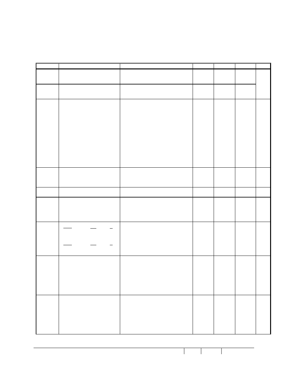
Solomon Systech
Aug 2002
P 32/43 Rev 1.0
SSD1854
10 DC CHARACTERISTICS
Table 10 - DC Characteristics (Unless otherwise specified, Voltage Referenced to V
SS
, V
DD
= 1.8 to
3.3V, T
A
= -20 to 85
�C)
Symbol Parameter
Test
Condition
Min
Typ
Max Unit
V
DD
Logic Circuit Supply Voltage
Range
V
CI
Booster Voltage Supply Pin
(Absolute value referenced to V
SS
) 1.8
- 3.3
V
REF
Internal Reference Voltage
(25
o
C, -0.10%/
o
C)
Internal Reference Voltage Source
Enabled (REF pin pulled High),
V
EXT
pin NC.
- 2.1 -
V
I
AC
Access Mode Supply Current
Drain (V
DD
Pin)
V
DD
= 2.7V, Voltage Generator On,
4X DC-DC Converter Enabled,
Write accessing, T
cyc
=3.3MHz,
Osc. Freq.=120kHz, Display On.
- 450
550
�A
I
DP1
Display Mode Supply Current
Drain (V
DD
& V
CI
Pins)
V
DD
= V
CI
= 2.7V, Voltage
Generator On, 4X DC-DC
Converter Enabled. Read/Write
Halt, Osc.
Freq. = 120kHz, Display
On, V
L7
= 13.8V.
- 550
900
�A
I
SB
Standby Mode Supply
Current Drain
V
DD
= 2.7V, LCD Driving Waveform
Off, Oscillating Freq. = 120kHz,
Read/Write halt.
- 90
130
�A
I
SLEEP
Sleep Mode Supply Current
Drain (VDD Pins)
V
DD
= 2.7V, LCD Driving Waveform
Off, Oscillator Off, Read/Write halt.
- - 2
�A
V
CC
LCD Driving Voltage
Generator Output (V
CC
Pin)
Display On, Voltage Generator
Enabled, DC/DC Converter
Enabled, Regulator Enabled, Osc.
Freq. = 120kHz,
V
DD
- 17.0
V
V
OH1
Output High Voltage (D
0
-D
15
) I
out
= +100�A
0.8*V
DD
- V
DD
V
LCD
V
OL1
Output Low Voltage (D
0
-D
15
) I
out
= -100�A
0
-
0.2*V
DD
V
V
L7
Most positive LCD Driving
Voltage Source (V
L7
Pin)
Regulator and Bias Divider Enabled
(V
L7
voltage depends on Internal
contrast Control)
V
DD
- 17.0
V
V
L7
Most positive LCD Driving
Voltage Source (V
L7
Pin)
Regulator and Bias Divider Disable
-
Floating
-
V
V
IH1
Input high voltage
( RES , PS0-2, CS , E, D/ C ,
R/W, D
0
-D
15
, REF)
0.8*V
DD
- V
DD
V
V
IL1
Input low voltage
( RES , PS0-2, CS , E, D/ C ,
R/W, D
0
-D
15
, REF)
0
-
0.2*V
DD
V
V
L7
LCD Display Voltage Output
(V
L7
, V
L6
, V
L5
, V
L4
, V
L3
, V
L2
Pins)
Regulator and Bias Divider Enabled
-
-
17
V
V
L6
-
-
14.5 V
V
L5
-
-
11.5 V
V
L4
-
-
8.5 V
V
L3
-
-
7.15 V
V
L2
-
-
5.8 V
V
L7
LCD Display Voltage Input
(V
L7
, V
L6
, V
L5
, V
L4
, V
L3
, V
L2
Pins)
Voltage reference to V
SS
, External
Voltage Generator, Bias Diver
Disabled
V
L6
- 17
V
V
L6
V
L5
- V
L7
V
V
L5
V
L4
- V
L6
V
V
L4
V
L3
- V
L5
V
V
L3
V
L2
- V
L4
V
V
L2
V
SS
V
L3
V
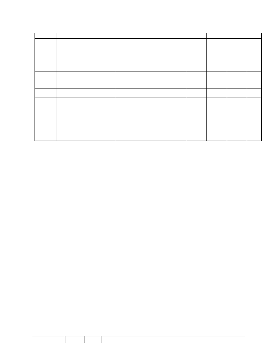
SSD1854
Rev 1.0
P 33/43 Aug 2002
Solomon Systech
Symbol Parameter
Test
Condition
Min
Typ
Max Unit
I
OH
Output High Current Source
(D
0
-D
15
)
Output Voltage=V DD -0.4V
50
-
-
�A
I
OL
Output Low Current Drain
(D
0
-D
15
)
Output Voltage = 0.4V
-
-
-50
�A
I
OZ
Output Tri-state Current
Source
(D
0
-D
15
)
-1
-
1
�A
I
IL
/I
IH
Input
Current
( RES , PS0-2, CS , E, D/ C ,
R/W, D
0
-D
15
, REF)
-1
-
1
�A
C
IN
Input
Capacitance
(all logic pins)
-
5
7.5
pF
V
L7
Variation of V
L7
Output (1.8V
< V
DD
< 3.5V)
Regulator and Bias Divider
Enabled, Internal Contrast Control
Enabled, Set Contrast Control
Register = 32
-2
0
+2
%
TC0
Temperature Coefficient 0*
Voltage Regulator Enabled
-0.06
-0.05
-0.04
%
TC2
Temperature Coefficient 2*
(POR)
Voltage Regulator Enabled
-0.11
-0.10
-0.09
%
TC4
Temperature Coefficient 4*
Voltage Regulator Enabled
-0.16
-0.15
-0.14
%
TC6
Temperature Coefficient 6*
Voltage Regulator Enabled
-0.22
-0.21
-0.20
%
* The formula for the temperature coefficient is:
TC(%)=
�
�100%
1
V
REF
at 25�C
V
REF
at 50�C � V
REF
at 0�C
50�C � 0�C
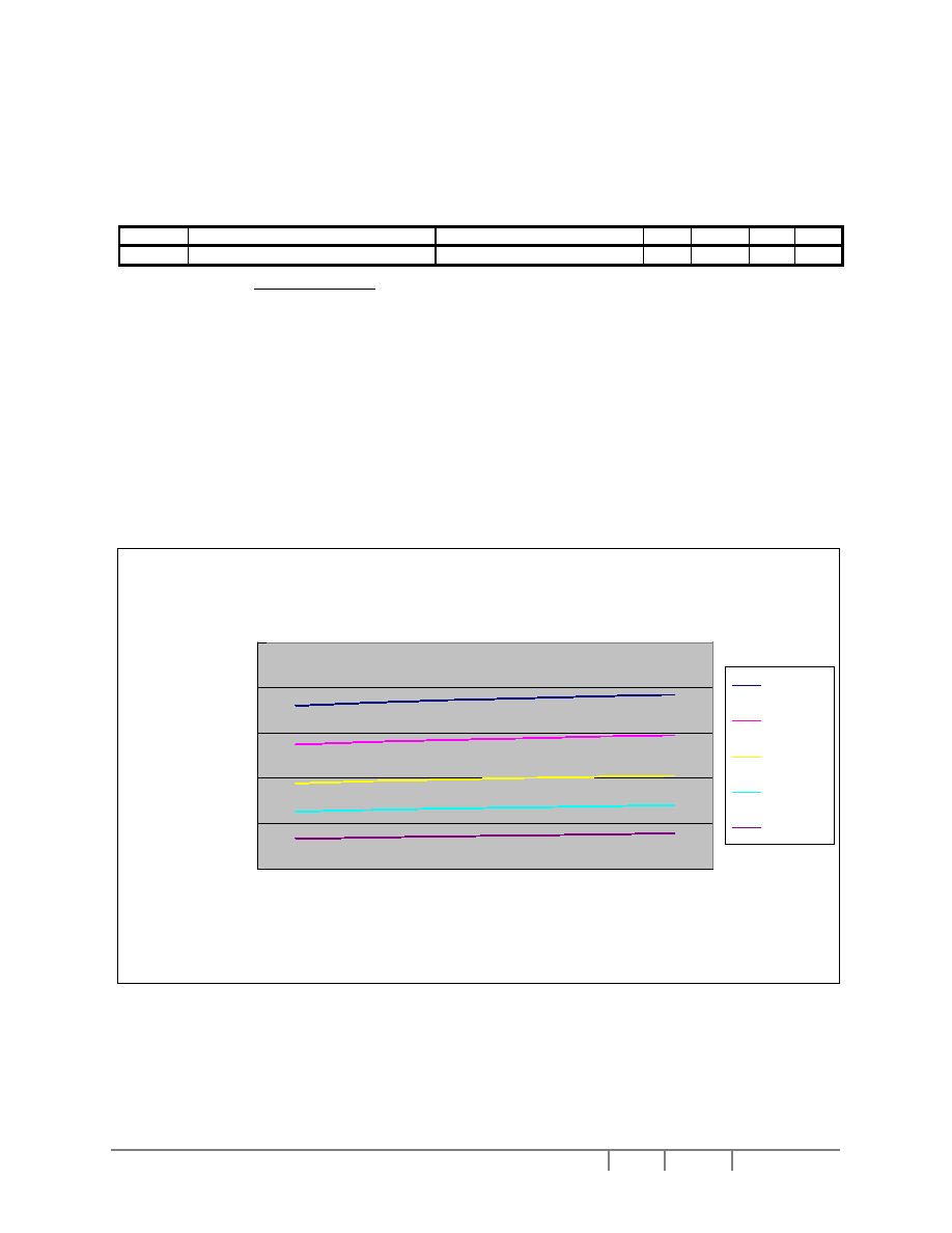
Solomon Systech
Aug 2002
P 34/43 Rev 1.0
SSD1854
11 AC CHARACTERISTICS
Table 11 - AC Characteristics (Unless otherwise specified, Voltage Referenced to V
SS
, V
DD,
V
CI
= 2.7V,
T
A
= -20 to 85
�C)
Symbol Parameter
Test
Condition
Min
Typ
Max
Unit
F
osc
Variation of Oscillation Frequency
Oscillator Resistor = 680K
-10 - +10
%
Frame Frequency =
MUX
)
1
PWM
(
F
OSC
�
+
where
F
osc
is the oscillation Frequency
PWM is the Pulse Width Modulation level
MUX is the multiplex ratio
Example 1:
F
osc =
120KHz; PWM = 9 level; MUX = 160
Frame Frequency = 75 Hz
Example 2:
F
osc =
120KHz; PWM = 15 level; MUX = 128
Frame Frequency = 58.6 Hz
Oscillation Frequency at different VDD
60.00
90.00
120.00
150.00
180.00
210.00
1.8
2.1
2.4
2.7
3
3.3
VDD (V)
O
s
cillation F
r
equency (
K
H
z
)
470K
560K
680K
820K
1000K
Figure 8 - Oscillation Frequency at different VDD at 25
�
�
�
�
C
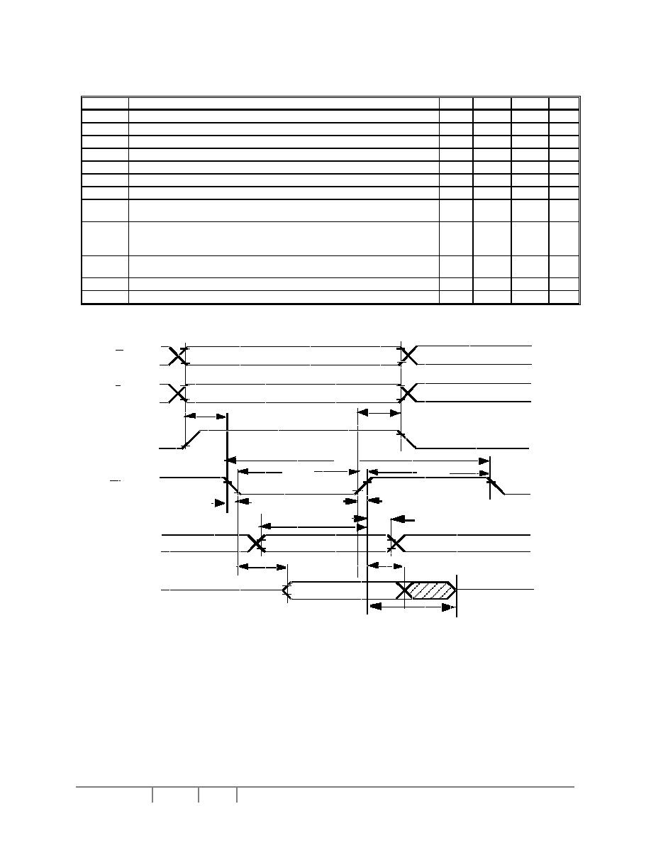
SSD1854
Rev 1.0
P 35/43 Aug 2002
Solomon Systech
Table 12 � Parallel Timing Characteristics 1
(T
A
= -20 to 85
�C, V
DD
= 1.8 to 3.3V, V
SS
=0V)
Symbol Parameter Min
Typ
Max
Unit
t
cycle
Clock Cycle Time (write cycle)
166
-
-
ns
t
AS
Address Setup Time
0
-
-
ns
t
AH
Address Hold Time
0
-
-
ns
t
DSW
Write Data Setup Time
30
-
-
ns
t
DHW
Write Data Hold Time
5
-
-
ns
t
DHR
Read Data Hold Time
15
-
-
ns
t
OH
Output Disable Time
-
-
50
ns
t
ACC
Access Time (RAM)
Access Time (command)
-
-
-
-
140
140
ns
PW
CSL
Chip Select Low Pulse Width (read RAM)
Chip Select Low Pulse Width (read Command)
Chip Select Low Pulse Width (write)
70
70
70
-
-
-
-
-
-
ns
PW
CSH
Chip Select High Pulse Width (read)
Chip Select High Pulse Width (write)
40
40
-
-
-
-
ns
t
R
Rise Time
-
-
10
ns
t
F
Fall Time
-
-
10
ns
Valid Data
t
cycle
t
DSW
t
AS
t
AH
t
DHR
t
ACC
CS
D/
C
D
0
-D
7
E
Valid Data
D
0
-D
7
(Write data to driv er)
(Read data f rom driv er)
t
DHW
PW
CSL
PW
CSH
t
F
t
R
R/
W
t
OH
Figure 9 � Parallel 6800-series Interface Timing Characteristics (PS0 = H, PS1 = H)
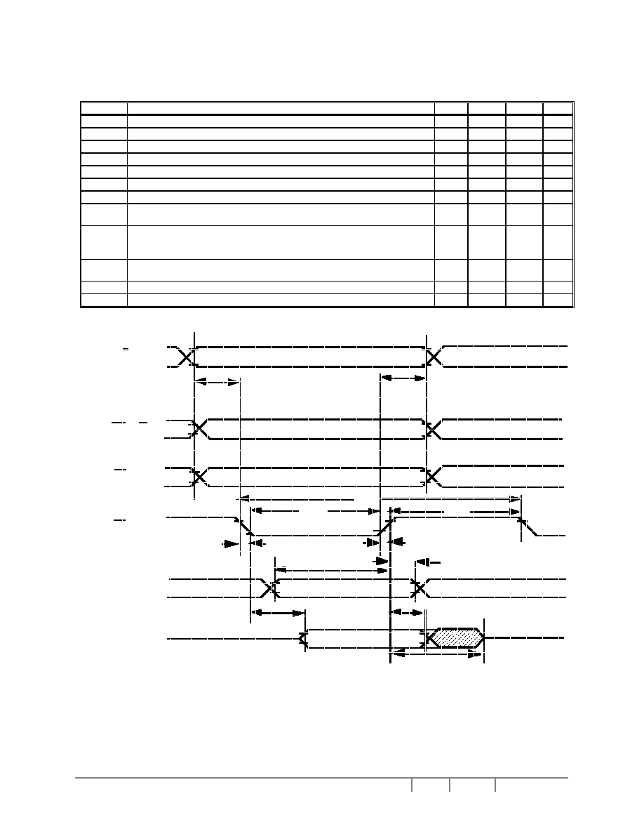
Solomon Systech
Aug 2002
P 36/43 Rev 1.0
SSD1854
Table 13 � Parallel Timing Characteristics 2
(T
A
= -20 to 85
�C, V
DD
= 1.8 to 3.3V, V
SS
=0V)
Symbol Parameter Min
Typ
Max
Unit
t
cycle
Clock Cycle Time (write cycle)
166
-
-
ns
t
AS
Address Setup Time
0
-
25
ns
t
AH
Address Hold Time
0
-
-
ns
t
DSW
Write Data Setup Time
30
-
-
ns
t
DHW
Write Data Hold Time
5
-
-
ns
t
DHR
Read Data Hold Time
15
-
-
ns
t
OH
Output Disable Time
-
-
50
ns
t
ACC
Access Time (RAM)
Access Time (command)
-
-
-
-
140
140
ns
PW
CSL
Chip Select Low Pulse Width (read RAM)
Chip Select Low Pulse Width (read Command)
Chip Select Low Pulse Width (write)
70
70
70
-
-
-
-
-
-
ns
PW
CSH
Chip Select High Pulse Width (read)
Chip Select High Pulse Width (write)
40
40
-
-
-
-
ns
t
R
Rise Time
-
-
10
ns
t
F
Fall Time
-
-
10
ns
Valid Data
t
cycle
t
D SW
t
AS
t
AH
t
D HR
t
AC C
CS
D/C
D
0
-D
7
RD (E)
Valid Data
D
0
-D
7
(Write data to driver)
(Read data from driver)
t
DH W
PW
CSL
PW
CSH
t
F
t
R
t
OH
WR (R/W)
Figure 10 - Parallel 8080-series Interface Timing Characteristics (PS0 = H, PS1 = L)

SSD1854
Rev 1.0
P 37/43 Aug 2002
Solomon Systech
Table 14 � Serial Timing Characteristics
(T
A
= -20 to 85
�C, V
DD
= 1.8 to 3.3V, V
SS
=0V)
Symbol
Parameter
Min Typ Max Unit
t
cycle
Clock Cycle Time
58.8
-
-
ns
t
AS
Address Setup Time
14
-
-
ns
t
AH
Address Hold Time
30
-
-
ns
t
CSS
Chip Select Setup Time
30
-
-
ns
t
CSH
Chip Select Hold Time
�*t
cycle
- - ns
t
DSW
Write Data Setup Time
30
-
-
ns
t
OHW
Write Data Hold Time
30
-
-
ns
t
CLKL
Clock Low Time
30
- - ns
t
CLKH
Clock High Time
30
- - ns
t
R
Rise Time
-
- 10 ns
t
F
Fall Time
-
-
10 ns
Valid Data
t
c ycle
t
DSW
t
AS
t
AH
SCK
D/C
SDA
CS
t
DHW
t
C LK L
t
C L KH
t
F
t
R
t
CSS
t
CS H
(Required if PS1 = H)
D7
D6
D5
D4
D3
D2
D1
D0
SCK
SDA
CS
Figure 11- Serial Timing Characteristics (PS0 = L)

Solomon Systech
Aug 2002
P 38/43 Rev 1.0
SSD1854
12 APPLICATION CIRCUIT
Figure 12 � LCD Pins Connection of SSD1854Z
DISPLAY PANEL SIZE
128 X 160
COM0
COM1
COM2
:
:
:
:
:
:
:
:
:
:
:
:
:
:
:
:
:
:
COM157
COM158
COM159
SEG0
.................................................................
SEG127
Segment Remapped
[Command: A1]
Remapped COM
SCAN Direction
[Command: C8]
:
:
:
:
:
:
:
:
SSD1854 IC
160 MUX
(DIE FACE IP)
:
:
:
:
:
:
SEG126
SEG127
:
:
:
:
:
:
:
:
:
:
:
:
:
SEG
1
SEG
0
COM0
COM1
COM2
COM3
:
:
:
:
:
:
:
:
:
:
:
:
:
:
:
:
:
:
:
:
:
:
:
:
C
O
M
159
C
O
M
158
C
O
M
157
:
:
:
:
:
:
:
RE
S
#
PS0 PS1 PS2 D/C R/
W
E RE
F
D0-
D
15
CS
#
VL
2
VL
3
VL
4
VL
5
VL
6
VL
7
CAP
CAN CBP
CBN CCP
CCN CDP
CDN VCC C3
P
C1
N
C1
P
C2
P
C2
N
C4
P
CONTROL
CIRCUIT
BOOSTER
CIRCUIT
REGULATOR
DIVIDER
CIRCUIT

SSD1854
Rev 1.0
P 39/43 Aug 2002
Solomon Systech
12.1 DC-DC Converter Circuit Configuration
*Note: Capacitor value = 1
�F to 4.7�F, which is depended on the LCD panel characteristic
12.2 Bias Divider Circuit Configuration
C
3P
C
1N
Vss
Vcc
C
1P
C
2P
C
2N
C
4P
SSD1854
IC
3x Converter
4x Converter
5x Converter
+
+
+
+
+
+
+
+
+
+
+
+
C
AP
C
AN
C
BP
C
BN
C
CP
C
CN
C
DP
C
DN
V
L7
V
L6
V
L5
V
L4
V
L3
V
L2
SSD1854
IC
+
+
+
+
+
+
+
+
+
+
V
SS
Internal Regulator and Bias Divider
[COMMAND: 2F]
Capacitor value
for C
AP
~C
DN
= 1
�
F to 2.2
�
F
Capacitor value
for V
L2
~V
L7
= 1
�
F
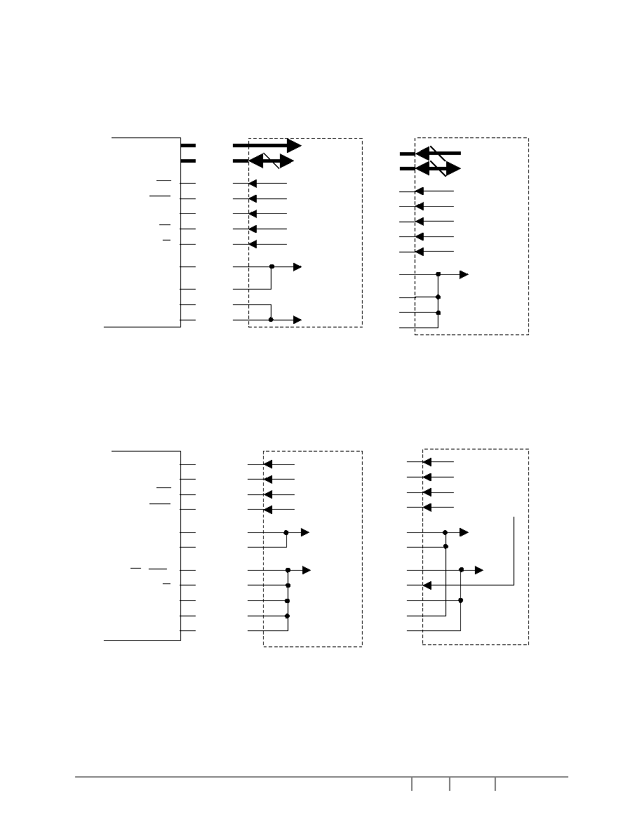
Solomon Systech
Aug 2002
P 40/43 Rev 1.0
SSD1854
12.3 Parallel Interface Configuration (Read / Write)
12.4 Serial Interface Configuration (Write Only)
D
7
(SDA)
D
6
(SCK)
CS
RES
REF
E
R/
W
( WR )
D/ C
PS0
PS1
PS2
SSD1854
IC
3-wire Interface
V
DD
V
SS
MCU
Control
signal
4-wire Interface
V
DD
V
SS
MCU
Control
signal
D
8
-D
15
D
0
-D
7
CS
RES
E
R/
W
D/ C
REF
PS0
PS1
PS2
SSD1854
IC
8080 Parallel Interface
(8-bits read and write)
MCU
Control
signal
V
DD
V
SS
6800 Parallel Interface
(8-bits read and 16-bits write)
MCU
Control
signal
V
DD
V
SS
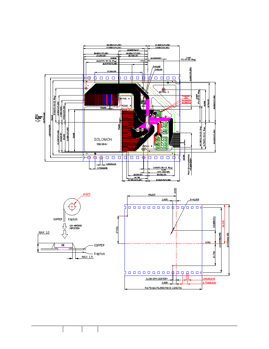
SSD1854
Rev 1.0
P 41/43 Aug 2002
Solomon Systech
13 APPENDIXA
Figure 13 � SSD1854U COF Drawing 1
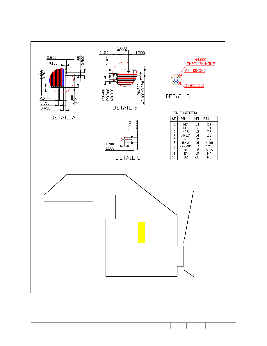
Solomon Systech
Aug 2002
P 42/43 Rev 1.0
SSD1854
Figure 14 � SSD1854U COF Drawing 2
N
C
N
C
SEG0
SEG1
.
.
.
.
S
E
G
126
S
E
G
127
N
C
N
C
NC
NC
COM0
COM1
COM2
.
.
.
.
COM157
COM158
COM159
NC
NC
NC
NC
CS#
RES#
D/C
RW(WR#)
E(RD#)
D0
D1
D2
D3
D4
D5
D6(SCK)
D7(SDA)
VDD
VCI
VSS
NC
NC
Note:
PS0, PS1, AVDD, DVDD, REF are
connected to VDD
PS2 is connected to VSS
Set Conditions
6800 8-bits Parallel Interface,
Internal Reference Voltage Source

SSD1854
Rev 1.0
P 43/43 Aug 2002
Solomon Systech
Solomon Systech reserves the right to make changes without further notice to any products herein. Solomon Systech makes no warranty,
representation or guarantee regarding the suitability of its products for any particular purpose, nor does Solomon Systech assume any liability arising
out of the application or use of any product or circuit, and specifically disclaims any and all liability, including without limitation consequential or
incidental damages. "Typical" parameters can and do vary in different applications. All operating parameters, including "Typicals" must be validated for
each customer application by customer's technical experts. Solomon Systech does not convey any license under its patent rights nor the rights of
others. Solomon Systech products are not designed, intended, or authorized for use as components in systems intended for surgical implant into the
body, or other applications intended to support or sustain life, or for any other application in which the failure of the Solomon Systech product could
create a situation where personal injury or death may occur. Should Buyer purchase or use Solomon Systech products for any such unintended or
unauthorized application, Buyer shall indemnify and hold Solomon Systech and its offices, employees, subsidiaries, affiliates, and distributors harmless
against all claims, costs, damages, and expenses, and reasonable attorney fees arising out of, directly or indirectly, any claim of personal injury or
death associated with such unintended or unauthorized use, even if such claim alleges that Solomon Systech was negligent regarding the design or
manufacture of the part.
http://www.solomon-systech.com