 | –≠–ª–µ–∫—Ç—Ä–æ–Ω–Ω—ã–π –∫–æ–º–ø–æ–Ω–µ–Ω—Ç: ACX302 | –°–∫–∞—á–∞—Ç—å:  PDF PDF  ZIP ZIP |

ACX302AK
8.80cm (3.5 Type) NTSC/PAL Color LCD Panel
Description
The ACX302AK is a 8.80cm diagonal active matrix
TFT-LCD panel addressed by low temperature
polycrystalline silicon transistors with built-in
peripheral driving circuitry. This panel provides full-
color representation for NTSC and PAL systems. In
addition, RGB dots are arranged in a delta pattern
that provides smooth picture quality without fixed
color patterns compared to vertical stripe and mosaic
patterns.
Features
∑ Number of active dots: 200,000, 8.80cm (3.5 Type) in diagonal
∑ Horizontal resolution:
440 TV lines
∑ Optical transmittance: 8.2% (typ.)
∑ High contrast ratio with normally white mode: 200 (typ.)
∑ Built-in H and V driving circuitry (built-in input level conversion circuit, 3V drive possible)
∑ Low voltage, low power consumption 12V drive: 60mW (typ.)
∑ Smooth pictures with a RGB delta arrangement
∑ Supports NTSC/PAL
∑ Built-in picture quality improvement circuit
∑ Up/down and/or right/left inverse display function
∑ 16:9 screen display function
∑ AR (anti-reflectance) surface treatment provides an easy-to-see display even outdoors
∑ Dirt-resistant surface treatment
∑ Narrow frame
∑ High color reproductivity
Element Structure
∑ Active matrix TFT-LCD panel with built-in peripheral driving circuitry using low temperature polycrystalline
silicon transistors
∑ Number of pixels
Total number of dots
: 884 (H)
◊
230 (V) = 203,320
Number of active dots
: 880 (H)
◊
228 (V) = 200,640
∑ Panel dimensions
Package dimensions
: 78.8 (W)
◊
63.3 (D)
◊
2.2 (H) (mm)
Effective display dimensions : 70.400 (H)
◊
52.725 (V) (mm)
Applications
LCD monitors, etc.
≠ 1 ≠
E99419A9Z-PS
Sony reserves the right to change products and specifications without prior notice. This information does not convey any license by
any implication or otherwise under any patents or other right. Application circuits shown, if any, are typical examples illustrating the
operation of the devices. Sony cannot assume responsibility for any problems arising out of the use of these circuits.

≠ 2 ≠
ACX302AK
Block Diagram
The panel block diagram is shown below.
LC
C
S
T
E
S
T
L
T
E
S
T
R
C
O
M
V
S
T
V
C
K
E
N
D
W
N
V
V
D
D
V
S
S
H
V
D
D
V
S
S
G
T
E
S
T
2
W
I
D
E
H
S
T
R
E
F
T
E
S
T
1
C
e
x
t
/
R
e
x
t
H
C
K
2
H
C
K
1
P
S
I
G
G
R
E
E
N
R
E
D
B
L
U
E
R
G
T
COM
2
3
4
5
6
7
8
9
10
11
12
13
14
15
16
18
19
20
21
22
23
1
24
17
V
S
h
i
f
t
R
e
g
i
s
t
e
r
V
S
h
i
f
t
R
e
g
i
s
t
e
r
V Level Shifter
Negative Voltage
Generation Circuit
Common
Voltage
H Level Shifter & Shift Register

≠ 3 ≠
ACX302AK
Absolute Maximum Ratings (Vss = 0V)
∑ H driver supply voltage
HV
DD
, Cext/Rext
≠1.0 to +17
V
∑ V driver supply voltage
VV
DD
≠1.0 to +15
V
∑ V driver negative supply voltage VSSG
≠3.0 to +1.0
V
∑ Common voltage of panel
COM
≠1.0 to +17
V
∑ H driver input pin voltage
HST, HCK1, HCK2, RGT, WIDE ≠1.0 to +17
V
∑ V driver input pin voltage
VST, VCK, EN, DWN, REF
≠1.0 to +15
V
∑ Video signal, uniformity improvement signal input pin voltage
GREEN, RED, BLUE, PSIG
≠1.0 to +13
V
∑ Operating temperature
Topr
≠10 to +60
∞C
∑ Storage temperature
Tstg
≠30 to +85
∞C
Operating Conditions
1. Input/output supply voltage conditions
1
(Vss = 0V)
Item
Supply voltage
HV
DD
VV
DD
Cext/Rext
2
VSSG
11.4
11.4
HV
DD
≠ 2.0
≠2.3
12.0/13.5
12.0/13.5
12.0/13.5
≠1.8
14.0
14.0
--
≠1.5
V
V
V
V
VSSG output voltage setting
3
Symbol
Min.
Typ.
Max.
Unit
1
The HV
DD
/VV
DD
typical voltage setting is noted as 12.0V in these specifications.
2
Connect the resistor and capacitor to the Cext/Rext pin as shown in the figure below.
3
For the VSSG output setting, connect an external smoothing capacitor and a voltage stabilizing Zener diode
as shown in the figure below.
HV
DD
≠ Cext/Rext
Cext/Rext
HV
DD
HV
DD
7
V
o
l
t
a
g
e
Time
t
ext
Set a Cext value that satisfies
t
ext > 1ms.
The Cext/Rext value differs
according to the rising time
of the panel supply voltage.
Rext
ACX302AK
HV
DD
VSSG
V
SS
Cext/Rext
1µF
Use a Zener
voltage of 2.7V.
(RD2.7UM is
recommended.)
Cext
≠ 4 ≠
ACX302AK
4
Input video and uniformity improvement signals should be symmetrical to VVC. The input conditions for the
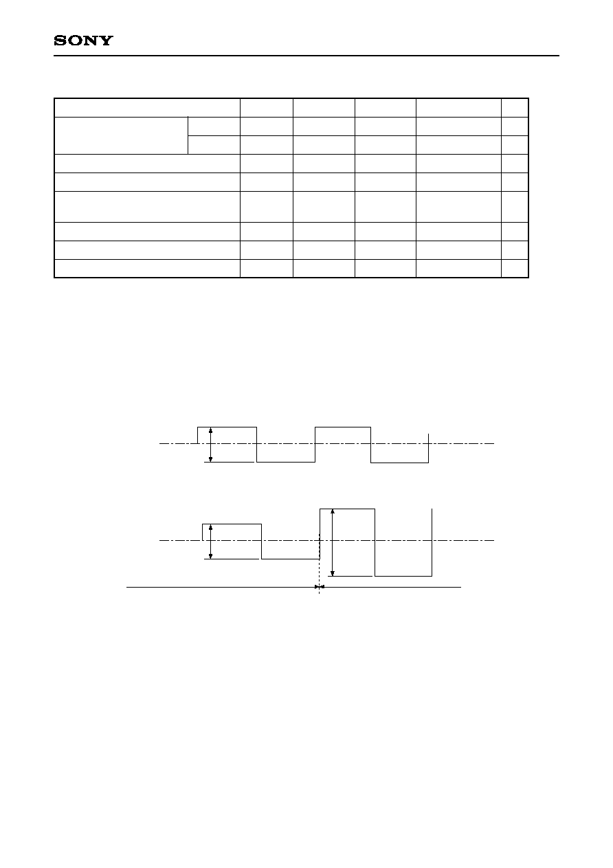
uniformity improvement signal Vpsig differ for 4:3 display and 16:9 display.
1) During 4:3 display, input the voltage amplitude symmetrical to VVC as shown in Fig. 1.
2) During 16:9 display, input the same signal amplitude as in 1) above during the effective display portion,
and input the black signal level VpsigBK during the top/bottom black input portion as shown in Fig. 2.
Item
H/V driver input voltage
(Low)
(High)
VIL
VIH
VREF
VVC
Vsig
Vpsig
VpsigBK
Vcom
≠0.3
2.6
VIH/2 ≠ 0.3
5.3
1.0
VVC ± 2.3
VVC ≠ 0.4
0.0
3.0
VIH/2
5.5
VVC ± 4.0
VVC ± 2.5
VVC ± 4.0
VVC ≠ 0.3
0.3
5.5
VIH/2 + 0.3
5.7
VV
DD
≠ 2.0
(however, 10V or less)
VVC ± 2.7
VVC ± 4.5
VVC ≠ 0.2
V
V
V
V
V
V
V
V
REF input voltage
Video signal center voltage
Video signal input range
Uniformity improvement signal
16:9 display top/bottom black signal
4
Common voltage of panel (Ta = 25∞C)
Symbol
Min.
Typ.
Max.
Unit
2. Input signal voltage conditions
(Vss = 0V)
During 4:3 display
PSIG
VVC
Vpsig
During 16:9 display
PSIG
VVC
Vpsig
VpsigBK
VVC ± 4.0V
VVC ± 2.5V
Top/bottom black display portion
(letterbox portion)
Effective display portion
Fig. 1
Fig. 2

≠ 5 ≠
ACX302AK
Pin
No.
1
2
3
4
5
6
7
8
9
10
11
12
TESTL
COM
VST
VCK
EN
DWN
VV
DD
V
SS
HV
DD
VSSG
TEST2
WIDE
13
14
15
16
17
18
19
20
21
22
23
24
HST
REF
TEST1
Cext/
Rext
HCK2
HCK1
PSIG
GREEN
RED
BLUE
RGT
TESTR
Start pulse input for H shift register
drive
Level shifter circuit REF voltage
input
Panel test output; no connection
Time constant power supply input
for H shift register drive
Clock input for H shift register drive
Clock input for H shift register drive
Uniformity improvement signal input
Video signal (G) input to panel
Video signal (R) input to panel
Video signal (B) input to panel
H shift register drive direction signal
input
Panel test output; no connection
Symbol
Description
Pin
No.
Symbol
Description
Panel test output; no connection
Common voltage input of panel
Start pulse input for V shift register
drive
Clock input for V shift register drive
Gate selection pulse enable input
V shift register drive direction signal
input
Power supply input for V driver
H and V driver GND
Power supply input for H driver
Negative power supply setting for
V driver
Test; no connection
Pulse input for 16:9 mode
Pin Description