 | –≠–ª–µ–∫—Ç—Ä–æ–Ω–Ω—ã–π –∫–æ–º–ø–æ–Ω–µ–Ω—Ç: ACX705AKM | –°–∫–∞—á–∞—Ç—å:  PDF PDF  ZIP ZIP |
ACX705AKM
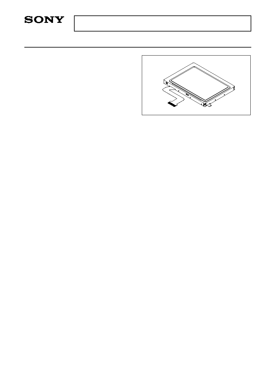
6.92cm Diagonal Reflective Color LCD Module
Description
The ACX705AKM is a 6.92cm diagonal active
matrix reflective color TFT-LCD module with a front
light unit and a driving board. This module provides
low power consumption which is realized by built-in
3-bit digital interface circuitry.
Features
∑ Number of dots:
240
◊
RGB
◊
160
∑ Dot size:
80µm
◊
240µm
∑ High reflectivity:
(25% typ.)
∑ High contrast ratio: (13:1 typ. at the condition of turning off the front light)
∑ Number of colors: 512
∑ Low power consumption (47mW typ.) with a driving board composed of a LCD controller IC,
a reference driver IC and a DC-DC convertor
∑ Built-in 3-bit digital interface circuitry
∑ Compact size
∑ Thin and bright front light unit
Element Structure
∑ Active matrix TFT-LCD panel with built-in peripheral driving circuitry using low temperature polycrystalline
silicon transistors
∑ Number of dots
Total number of dots:
242
◊
3 (H)
◊
162 (V) = 117,612
Number of active dots:
240
◊
3 (H)
◊
160 (V) = 115,200
∑ Dimensions
Module dimensions:
71.4mm
◊
52.0mm
◊
4.8mm (t) (parts area 6.5mm (t) max.)
Effective display dimensions: 57.6mm (H)
◊
38.4mm (V)
Applications
PDA, etc.
≠ 1 ≠
E00847-PS
Sony reserves the right to change products and specifications without prior notice. This information does not convey any license by
any implication or otherwise under any patents or other right. Application circuits shown, if any, are typical examples illustrating the
operation of the devices. Sony cannot assume responsibility for any problems arising out of the use of these circuits.

≠ 2 ≠
ACX705AKM
Absolute Maximum Ratings (Ta = 25∞C, V
SS
= 0V)
∑ Supply voltage
V
CC
1
V
SS
≠ 0.3 to +5.5
V
V
CC
2
V
SS
≠ 0.3 to +5.5
V
∑ Input voltage
V
I
V
SS
≠ 0.3 to V
CC
2 + 0.3
V
∑ Storage temperature
Tstg
≠30 to +70
∞C
∑ LED current
Iled
(as below)
Right
Left
Active area
Top
Bottom
Left
Right
Top
Front View
Rear View
Bottom
Pin 22
Pin 1
0
0
10
20
Allowable forward current
Iled [mA]
30
25
20
40
Ta [
∞
C]
60
80
100
Recommended Operating Conditions
∑ Supply voltage
V
CC
1
3.50 to 4.20
V
V
CC
2
2.55 to 3.15
V
∑ Operating temperature
Topr
≠10 to +60
∞C
Pin Location of Panel Block
The FPC pin assignment is described in on page 5. The location of Pin 1 is shown below.

≠ 3 ≠
ACX705AKM
Module Configuration
This module is composed of a reflective color TFT-LCD panel, a front light unit and a driving board as shown in
the figure below.
Rear View
Front View
Active area
center
ACX705AKM-7 T
ACX705AKM-01
71.4 (Outer frame)
8.1
[(75.5)]
57.6 (Active area)
(33.3)
60
+0.1
0
(Window)
(3.3)
38.1
(5.93)
(8.75)
30.5
(1.15)
4
8
7
11.5
6
5.5
(5.1)
(1.7)
(7.6)
52.6
0
≠0.1
(Parts area)
(11.3)
(7.5)
59.6
+0.1
0
(Window)
(6.3)
(5.5)
71.4
±
0.3 (Outer frame)
(59.4)
(2)
6.4
±
0.3
63.4 (Cover plate)
(1.6)
(2)
(7)
52
±
0.3 (Outer frame)
(6)
(9)
37
+0.1
0
(Window)
35
0 ≠0.1
(Parts area)
(10)
(4.08)
(40.2)
38.4 (Active area)
(24.48)
27.52
52
±
0.3
7.12
40.8
+0.1 0
(Window)
(5.9)
(26.4)
2
5.42
44.2 (Cover plate)
(2.38)
(2)

≠ 4 ≠
ACX705AKM
Block Diagram
The block diagram of this LCD module is shown below.
+9.0V
+5.0V
≠
6.5V
Control pulse
Control pulse
Control pulse
+5.0V
+3.0V
V
ref
VCOM
36
Data
RGB
◊
3-bit
◊
4
9
22
8
+9.0V
,
≠
6.5V
15mA
(25
∞
C)
Cover Plate
Front Light (LED)
H Driver
V Driver
H Driver
Poly-Si TFT
LCD
(240
◊
RGB
◊
160)
CXD3507GG
(LCD Controller)
DC-DC
Converter
CXD2475TQ
(Reference
V
oltage Driver)
MIC1
MIC2
Vcc1 (+3.8V)
Vcc2 (+3.0V)
Data in
(RGB
◊
3-bit)
Hsync
Vsync
MCK
S/D

≠ 5 ≠
ACX705AKM
Pin Description
Pin No.
Symbol
Description
1
2
3
4
5
6
7
8
9
10
11
12
13
14
15
16
17
18
19
20
21
22
MIC1
MIC2
V
CC
1
V
CC
1
GND
GND
R0
R1
R2
G0
G1
G2
B0
B1
B2
Hsync
Vsync
S/D
MCK
V
CC
2
LED V
DD
LED GND
+3.8V power supply
+3.8V power supply
Ground
Ground
Red data input (LSB)
Red data input
Red data input (MSB)
Green data input (LSB)
Green data input
Green data input (MSB)
Blue data input (LSB)
Blue data input
Blue data input (MSB)
Hsync input
Vsync input
Shut down
Master clock (4.2MHz)
+3.0V power supply
LED V
DD
LED GND

≠ 6 ≠
ACX705AKM
S/D
There are input for power up/down sequence.
Power Up Sequence
S/D
Inactive (low)
Vcc2
0
Active
MCK
Hsync
Vsync
DATA (in)
Invalid (low)
Vcc2
0
Vcc1, Vcc2
Vcc1, Vcc2
0
1 Field (typ.)
Valid
Vcc1, Vcc2
Active
Vcc1, Vcc2
0
In active (low)
Vsync
Vcc2
0
S/D
Vcc2
0
13 Fields
Power Down Sequence

≠ 7 ≠
ACX705AKM
Electrical Characteristics
Item
Supply voltage
Ripple voltage
Input voltage 1
Input voltage 2
Supply current
Input current 1
Current consumption
Total power consumption
Standby current
MCK frequency
Horizontal frequency
Vertical frequency
Data input pin capacitance
Hsync input pin capacitance
Vsync input pin capacitance
MCK input pin capacitance
S/D input pin capacitance
V
CC
1
V
CC
2
V
RF
V
H1
V
L1
Vt
+
Vt
≠
Vt
+
≠ Vt
≠
Iled
| I
H1
|
| I
L1
|
I
CC
1
I
CC
2
P
I
CC
1s
I
CC
2s
f
MCK
fh
fv
Cdata
Chsde
Cvs
Cmck
Csd
3.50
2.55
--
2.0
--
--
0.5
0.2
--
--
--
--
--
--
--
--
--
--
--
--
--
--
--
--
3.80
3.00
--
--
--
--
--
--
15
--
--
11.0
1.6
47
0.1
40
3.26
12.0
60.0
--
--
--
--
--
4.20
3.15
100
--
0.7
2.2
--
--
--
1.0
1.0
17.0
4.0
77
10
200
4.20
15.4
77.2
20
20
20
20
20
V
V
mV
V
V
V
V
V
mA
µA
µA
mA
mA
mW
µA
µA
MHz
kHz
Hz
pF
pF
pF
pF
pF
V
CC
1
V
CC
2
V
CC
1
MCK
(LVTTL level input)
All input pins excluding MCK
(LVTTL level Schmitt trigger
input)
LED V
DD
All input pins
V
CC
1
V
CC
2
R0 to R2, G0 to G2, B0 to B2
Hsync
Vsync
MCK
S/D
Symbol
Min.
Typ.
Max.
Unit
Pins
V
I
= V
CC
2
V
I
= 0V
8-pixel
◊
8-pixel Black and White checker pattern

≠ 8 ≠
ACX705AKM
Operating Conditions
Item
Symbol
Min.
Typ.
Max.
Unit
Master clock period
MCK width high
MCK width low
Data setup to MCK falling edge
Data hold from MCK falling edge
Hsync setup to MCK falling edge
Hsync pulse width low
Vsync falling edge to Hsync falling edge phase difference
Vsync pulse width low
tclk
tch
tcl
tds
tdh
thss
thsw
tvhde
tvsw
1
--
--
10
15
10
9
254
2
--
0.5
0.5
--
--
--
--
--
--
--
--
--
--
--
--
16
269
20
tclk
tclk
tclk
ns
ns
ns
tclk
tclk
line
Operating Condition of Front Light
Item
Symbol
Min.
Typ.
Max.
Unit
LED current
Iled
--
15
--
mA
Lamp Life
The lamp life shall be greater than 50 hours. The operating lamp life is defined as having ended when the
illumination of light has reached 50% of the initial value.

≠ 9 ≠
ACX705AKM
Horizontal Timing Chart
227
228
229
231
232
233
234
236
237
238
239
230
235
240
123
5678
1
0
1
1
49
230
235
240
245
250
255
260
265
16 dots
16 dots
Hsync
D
ATA
MCK
Hsync
D
ATA
270
0
5
272 dots
tclk
tch
tcl
tds
tdh
thss
thsw
1
2
240

≠ 10 ≠
ACX705AKM
Vertical Timing Chart
160
155
165
180
185
190
195
5
0
20 lines
20 lines
Vsync
Hsync
Hsync
Vsync
D
ATA
10
200 lines
tvhde
tvsw

≠ 11 ≠
ACX705AKM
Color Combination Table
Color
Black
Blue
Green
Cyan
Red
Magenta
Yellow
White
Black
Dark
Bright
Red
Black
Dark
Bright
Green
Black
Dark
Bright
Blue
--
--
--
--
--
--
--
--
0
1
2
3
4
5
6
7
0
1
2
3
4
5
6
7
0
1
2
3
4
5
6
7
Data signal
0
0
0
0
1
1
1
1
0
1
0
1
0
1
0
1
0
0
0
0
0
0
0
0
0
0
0
0
0
0
0
0
0
0
0
0
1
1
1
1
0
0
1
1
0
0
1
1
0
0
0
0
0
0
0
0
0
0
0
0
0
0
0
0
0
0
0
0
1
1
1
1
0
0
0
0
1
1
1
1
0
0
0
0
0
0
0
0
0
0
0
0
0
0
0
0
0
0
1
1
0
0
1
1
0
0
0
0
0
0
0
0
0
1
0
1
0
1
0
1
0
0
0
0
0
0
0
0
0
0
1
1
0
0
1
1
0
0
0
0
0
0
0
0
0
0
1
1
0
0
1
1
0
0
0
0
0
0
0
0
0
0
1
1
0
0
1
1
0
0
0
0
0
0
0
0
0
0
0
0
1
1
1
1
0
0
0
0
0
0
0
0
0
1
0
1
0
1
0
1
0
0
0
0
0
0
0
0
0
0
0
0
0
0
0
0
0
1
0
1
0
1
0
1
0
1
0
1
0
1
0
1
0
0
0
0
0
0
0
0
0
0
0
0
0
0
0
0
0
0
1
1
0
0
1
1
0
1
0
1
0
1
0
1
0
0
0
0
0
0
0
0
0
0
0
0
0
0
0
0
0
0
0
0
1
1
1
1
R0
Gray scale
R1
R2
G0
G1
G2
B0
B1
B2
Standard
color
Red
Green
Blue
Gray Scale
0
1
2
3
4
5
6
7

≠ 12 ≠
ACX705AKM
Color Coding
The color filters are coded in vertical stripe arrangement.
The shaded area is used for the dark border around the display.
Active area
240
◊
RGB
1
◊
RGB
1
◊
RGB
Front view
1
160
1
∑ ∑ ∑ ∑ ∑ ∑ ∑ ∑ ∑ ∑ ∑ ∑ ∑ ∑ ∑ ∑ ∑ ∑ ∑ ∑ ∑ ∑ ∑ ∑ ∑
∑ ∑ ∑ ∑ ∑ ∑ ∑ ∑ ∑ ∑ ∑ ∑ ∑ ∑ ∑ ∑ ∑ ∑ ∑ ∑ ∑ ∑ ∑ ∑ ∑
∑∑∑∑∑∑∑∑∑
∑∑∑∑∑∑∑∑∑
G
R
R
B
B
G
G
R
R
B
B
G
G
R
R
B
B
G
G
R
R
B
B
G
G
R
R
B
B
G
G
R
R
B
B
G
G
R
R
B
B
G
G
R
R
B
B
G
Scanning Direction
The scanning direction for the horizontal period and for the vertical period are A and B respectively as shown
below.
These scanning directions are from a front view.
Active area
Horizontal direction
A
Front view
vertical direction
B

≠ 13 ≠
ACX705AKM
Electro-optical Characteristics
Ta = 25∞C, With front light turning off
Item
Reflectivity
Contrast ratio
White chromaticity
Response time
Viewing angle
x
y
rise
fall
Top-Bottom
Left-Right
R
CR
xfloff
yfloff
Tr
Tf
VAtb
VAlr
20
10
0.28
0.29
--
--
90
100
25
13
0.30
0.31
5
10
100
120
--
--
0.32
0.33
40
40
--
--
%
CIE
CIE
ms
ms
degree (∞)
degree (∞)
1
2
3
4
5
Symbol
Min.
Typ.
Max.
Unit
Notes
Item
Luminance
Luminance uniformity
White chromaticity
x
y
Lcfl
Flunif
xflon
yflon
3.3
--
0.27
0.27
5
1.3
0.32
0.32
--
1.7
0.37
0.37
cd/m
2
CIE
CIE
6
7
3
Symbol
Min.
Typ.
Max.
Unit
Notes
Ta = 25∞C, With front light turning on (Iled = 15mA)

≠ 14 ≠
ACX705AKM
Notes:
1. Reflectivity (R)
In the Measurement system-1 (see Fig. 1 (a), (b)), calculate the reflectance factor by using the formula (1).
R = R (White) =
◊
reflectance factor of the reflectance standard ...(1)
2. Contrast ratio with front light turned off (CR)
In the Measurement system-1 (see Fig. 1 (a), (b)), measure the reflectance factor of "White" and "Black"
respectively and calculate by using the formula (2).
CR = ...(2)
3. White chromaticity
In the Measurement system-2 (see Fig. 2), measure the white chromaticity. The illumination source and
viewing area are D65 and 2∞ respectively.
4. Response time
In the Measurement system-3 (see Fig. 3), measure the electro-optical response time.
5. Viewing angle
In the Measurement system-1 (see Fig. 1 (c)), viewing area is defined by the area which makes the CR
2.
6. Luminance
In the Measurement system-4 (see Fig. 4), measure the luminance and calculate using the following formula
(3).
Lcfl = (Luminance (1) + Luminance (3) + Luminance (5) + Luminance (7) + Luminance (9))/5 ...(3)
7. Luminance uniformity
In the Measurement system-4 (see Fig. 4), measure the luminance and calculate using the following formula
(4).
Flunif = Luminance (maximum spot)/Luminance (minimum spot) ...(4)
Basic Measurement Conditions
(1) Driving voltage
Typical condition
(2) Measurement temperature
+25∞C unless otherwise specified.
(3) Measurement point
One point on the center of the panel unless otherwise specified.
(4) Light source and viewing area
D65 and 2∞
(5) Display "White": All R, G and B signal data are high (signal amplitude across the liquid crystal: ±1.0V).
Display "Black": All R, G and B signal data are low (signal amplitude across the liquid crystal: ±4.5V).
Front light is turned off unless otherwise specified.
Output from the "White" displayed panel
Output from the reflectance standard
R (White)
R (Black)

≠ 15 ≠
ACX705AKM
Left
Right
Top
= 30
∞
= 0
∞
Bottom
Optical
Detector
Driving Circuit
LCD panel
Optical fiber
Light source
Mearurement
Equipment
T
R
B
L
Left
Right
Top
FPC side
FPC side
= 0
∞
Bottom
(a)
(b)
(c)
Fig. 1. Measurement system-1
LCD panel
Integrated sphere
Optical fiber
Light Source
Optical
Detector
Mearurement
Equipment
Fig. 2. Measurement system-2

≠ 16 ≠
ACX705AKM
Oscilloscope
Optical Detector
Light sourse
LCD panel
30
∞
Tr
100%
Display Data
Optical
Instruments
Response
White (1111)
White (1111)
Black (0000)
Tf
90%
10%
0%
Time
Fig. 3. Measurement system-3

≠ 17 ≠
ACX705AKM
Illuminance
Colorimeter
BM-5A
Reflective
LCD Module
1
∞
(a) The apparatus for luminance measurement
(b) The spot locations for luminance measurement
400
±
50mm
1
2
3
4
5
6
7
8
9
K/6
L/6
L/3
L
L/3
L/6
K/3
K/3
K/6
K
Fig. 4. Measurement system-4

≠ 18 ≠
ACX705AKM
Cross Modulation
Cross modulation (cross talk) shall be inspected with following test pattern with 2% ND filter. Pattern is black
box 80 pixels wide and 120 pixels in length at minimum luminance, centered horizontally and vertically in the
active area. The remainder of the screen is 50% gray.
There shall be no visible difference of luminance around the black box through 2% ND filter.
H/4
H/2
H/4
H/4
H/4
H/2
Image Persistence
Display a completely white screen for 20 minutes and continuously display the test pattern shown below for a
minimum of two hours. Then display a completely white screen. A visible image of the box pattern shall not
persist more than two seconds viewed through 2% ND filter. Pattern is black box 80 pixels wide and 120 pixels
in length at minimum luminance, centered horizontally and vertically in the active area. The remainder of the
screen is white.

≠ 19 ≠
ACX705AKM
Notes on Handling
(1) Static charge prevention
Be sure to take the following protective measures. TFT-LCD panels are easily damaged by static charges.
a) Use non-chargeable gloves, or simply use bare hands.
b) Use an earth-band when handling.
c) Do not touch any electrodes of a panel.
d) Wear non-chargeable clothes and conductive shoes.
e) Install grounded conductive mats on the working floor and working table.
f) Keep panels away from any charged materials.
g) Use ionized air to discharge the panels.
(2) Protection from dust and dirt
a) Operate in a clean environment.
b) Do not touch the front light surface. The surface is easily scratched.
c) Use ionized air to blow dust off the panel.
(3) Others
a) Do not twist or bend the flexible PC board especially at the connecting region because the board is
easily deformed.
b) Do not drop the module.
c) Do not twist or bend the module.
d) Keep the module away from heat sources.
e) Do not dampen the module with water or other solvents.
f) Avoid storage or using the module at high temperature or high humidity, as this may result in damage.

≠ 20 ≠
ACX705AKM
Sony Corporation
Package Outline
Unit: mm
Active area center
ACX705AKM-7
T
ACX705AKM-01
4
5
3
2
1
6
71.4 (Outer frame)
8.1
(75.5)
57.6 (Active area)
(33.3)
60
+0.1
0
(Window)
(3.3)
38.1
(5.93)
(8.75)
30.5
(1.15)
4
8
7
1
1.5
6
5.5
(6.3)
(1.7)
8
52.6
0
-0.1
( Parts area)
(1
1.3)
(7.5)
59.6
+0.1
0
(Window)
(6.3)
(5.5)
71.4
±
0.3
(Outer frame)
(59.4)
(2)
6.4
±
0.3
63.4 (Cover plate)
(1.6)
(2)
0.3
±
0.5
(7)
52
±
0.3
(Outer frame)
(6)
(9)
37
+0.1
0
(Window)
35
0
-0.1
(Parts area)
(10)
(4.08)
(40.2)
38.4 (Active area)
(24.48)
27.52
52
±
0.3
7.12
40.8
+0.1
0
(Window)
(5.9)
(26.4)
2
5.42
44.2 (Cover plate)
(2.38)
(2)
1
F
ront sheild case
2
R
ear sheild case
3
F
lexible cable
4
D
riving board
5
L
abel
6
C
over plate
Note 1) Tolerance with no indicatin (
±
0.1)
2) : control dimension (minimum)