
CXA1203M/N
8mm VCR PAL JOG
Description
The CXA1203M/N compensates the color alignment
in variable speed mode for PAL-system 8mm VCRs.
This IC is also available for the SECAM system with
the built-in SECAM detector and BELL and C-BELL
filters.
Features
∑ Color alignment compensation which does not
require 1H delay line
∑ No AFC (f
H
) adjustment necessary
∑ Built-in SECAM detector
∑ Built-in BELL and C-BELL filters
∑ Available for the PAL-M system
Functions
V-Invert circuit, TH/DL APC, 2fsc PLL, SQ DET,
EX burst circuit, AFC (f
H
), Timing generator,
SECAM detector, BELL filter, C-BELL filter
Structure
Silicon monolithic IC
Absolute Maximum Ratings (Ta = 25∞C)
∑ Supply voltage
V
CC
7.0
V
∑ Operating temperature Topr
≠20 to +75
∞C
∑ Storage temperature
Tstg
≠55 to +150
∞C
∑ Allowable power dissipation
P
D
CXA1203M
567
mW
CXA1203N
536
mW
Recommended Operating Conditions
Supply voltage
4.5 to 5.5
V
(5.0V typ.)
≠ 1 ≠
E01Z33-PS
Sony reserves the right to change products and specifications without prior notice. This information does not convey any license by
any implication or otherwise under any patents or other right. Application circuits shown, if any, are typical examples illustrating the
operation of the devices. Sony cannot assume responsibility for any problems arising out of the use of these circuits.
CXA1203M
24 pin SOP (Plastic)
CXA1203N
24 pin SSOP (Plastic)

≠ 2 ≠
CXA1203M/N
Block Diagram and Pin Configuration
PB
PB
REC (Se)
PB (PAL)
PB (Se)
REC
TH/DL
SWD
1/2FHM
TH/DL
(1/2FHTA)
PAL-M
BF
BF
PAL-M
PAL
CW
BF Xch
TH/DL
(1/2FHTA)
DL
TH
XPB
MASK 75
≠
1
MASK
75
≠
2
U ERRI
1/2FHM
PAL-M
TH/DL
XFHM
1/2FHM
1/2FHM
SA CONT
CLG PLS
CLP PLS
SWD
1/2FHT
1/2
FHT
SECAM
DETPLS
TEST
RST
Normal
SECAM
BELL IN
SECAM IN
H ID
Normal
1/2FHTAB
SWD1/2FHM
SWD1/2FHT
D ERRI
XSHP
BELL
FILTER
24
ADJ
23
BELL IN
22
MODE
21
SECAM
IN
20
DL GAIN
ADJ
19
fsc IN
18
SQ ID
17
DL APC
LPF
16
C OUT
15
IREF
14
VREG
13
V
CC
1
PB C IN
2
SECAM
ACK
3
1/2FHMP
4
75% C
5
DLDP
6
SECAM
JUMP
7
SECAM
LPF
8
AFC
LPF
9
HD
10
C Sync
11
GND
12
MODE
C-BELL
BELL
AMP
≠
90
∞
VCO
S/H
Peak
Hold
LPF2
S/H
75%
MASK2
75%
MASK1
EDGE
TRIG
EDGE
TRIG
Secam
P. D.
Jump
P. D.
HD
AFC
ID
D
V-I1
◊
2
SQ
P.D.
LPF1
LPF
CONT
Clamp
LPF1
FM
DEMOD
LPF3
CONV1
Dummy
LIM
LIM1
LIM2
V-I2
LPF2
SW
MAIN
SW
BF
Gen
75%
150%
D
1/2
D

≠ 3 ≠
CXA1203M/N
Pin Description
Pin
No.
Symbol
1
V
CC
5.0V
(typ.)
--
--
Supply voltage pin
2
PB C
IN
350mVp-p
150mVp-p
(burst)
Input pin of PAL playback
chrominance signal.
The chroma ACK operates to
cut off the output at Pin 15
when the DC bias voltage at
Pin 2 is 0.7V or less.
3
SECAM
ACK
3.8V
(H)
0V
(L)
--
SECAM detector output pin.
H
SECAM
L
PAL
The SECAM or PAL mode is
fixed by applying an external
DC voltage.
SECAM: 3.0 to 5.0V
PAL: 0 to 1.0V
4
1/2
FHMP
--
--
Output pin of the pulse
obtained by dividing down the
AFC (f
H
-PLL) output by 2.
5
75% C
Connecting pin of the
charging and discharging
capacity to produce the
triangular wave chronized
with the C Sync signal.
All timing pulses used in the
IC are produced from this
triangular wave.
Voltage
Equivalent circuit
Description
DC
AC
3.2V
1.7V
3.5V
1.0V
3.0V
60k
47k
15.2p
2
PR
V
CC
V
CC
3
20k
20k
10k
8k
PR
(Sub)
4
4k/2
(
◊
2)
(
◊
2)
PR
V
CC
5
20k/3
(
◊
3)
(Sub)
(
◊
3)
28k
8k
PR
V
CC

≠ 4 ≠
CXA1203M/N
Pin
No.
Symbol
6
DLDP
1.4Vp-p
Input pin to switch the polarity
of the 1/2FHT pulse for the
SECAM detector.
Output pin of the AFC ID
signal in TEST mode
1
.
7
SECAM
JUMP
2.8V
(H)
1.4V
(L)
2.8V
(H)
1.4V
(L)
1.4Vp-p
--
--
Output pin to switch the
polarity of the 1/2FHT pulse.
Mode selection
1
is possible
by applying an external DC
voltage.
PAL-M: 0 to 0.5V
Normal: OPEN
RESET: 3.6 to 4.1V
TEST: 4.3 to 5.0V
8
SECAM
LPF
2.5V
Connecting pin of the time
constant of the LPF for the
SECAM detector.
9
AFC
LPF
2.0V
Connecting pin of the time
constant of the LPF for the
AFC (f
H
-PLL).
Voltage
Equivalent circuit
Description
DC
AC
6
8k
PR
V
CC
10k
10k
20k
20k
100k
7
PR
(Sub)
V
CC
8
4k
4k
PR
(Sub)
2k
100k
V
CC
9
4k/2
10k
6.5k
10k
PR
20k
1k
1k
(Sub)
(Sub)
(
◊
2)
(
◊
4)
V
CC

≠ 5 ≠
CXA1203M/N
Pin
No.
Symbol
10
HD
--
Output pin of the HD pulse
produced in the AFC (f
H
-PLL).
11
C Sync
--
--
Input pin of the composite
sync signal.
The internal threshold voltage
is 2.0V and the polarity is
active HIGH.
GND pin
13
VREG
4.2V
Output pin of the regulated
voltage source in the IC
(4.2V).
14
IREF
2.1V
Connecting pin of the
standard resistance to
produce the reference
current source in the IC.
Voltage
Equivalent circuit
Description
DC
AC
10
20k
PR
1k
(
◊
2)
(Sub)
(
◊
2)
V
CC
11
PR
20k
46k
20k
13
23p
Connected to
about 30
elements
(
◊
32)
V
CC
14
10k
PR
(Sub)
(
◊
2)
IREF
4k
40k
8k
V
CC
4.0V
0.4V
2.0V
12
GND
--
--
--

≠ 6 ≠
CXA1203M/N
Pin
No.
Symbol
16
DL APC
LPF
2.4V
--
Connecting pin of the time
constant of the LPF for the
TH/DL APC loop.
The TH/DL lock phase can
be varied by applying an
external DC current.
17
SQ ID
4.0V
(H)
0V
(L)
--
350mVp-p
Output pin of the SQ detector.
The TH or DL output signal at
Pin 15 can be selected by
applying an external DC
voltage.
DL: 0 to 2.0V
TH: 3.0 to 5.0V
18
fsc IN
--
Input pin of the fsc.
(chrominance subcarrier)
Voltage
Equivalent circuit
Description
DC
AC
16
PR
PR
V
CC
17
10k
PR
8k
20k
(Sub)
V
CC
18
PR
4k
30k
10.4p
V
CC
In PAL
mode
350mVp-p
150mVp-p
(burst)
15
C OUT
2.1V
Output pin of the playback
PAL signal (TH, DL and EX
burst)
2
, SECAM signal and
PAL-M signal.
(
◊
4)
15
PR
2.5k
V
CC

≠ 7 ≠
CXA1203M/N
Pin
No.
Symbol
21
MODE
--
--
Mode selection
1
is possible
by applying an external DC
voltage.
REC: 0 to 1.3V
PB: 1.7 to 2.8V
JOG: 3.2 to 5.0V
22
BELL
IN
--
83mVp-p
(SECAM
burst)
117mVp-p
(PAL
burst)
Input pin of the SECAM
signal.
Input pin of the SECAM
detector in playback mode.
Voltage
Equivalent circuit
Description
DC
AC
21
PR
8k
(Sub)
V
CC
22
PR
13.5k
15k
38k
15.2p
15.2p
100k
4k
V
CC
150mVp-p
(burst)
19
DL GAIN
ADJ
5.0V
(typ.)
Control pin of the DL signal
gain.
The gain can be varied by
applying an external DC
voltage. The internally fixed
gain is obtained at 5.0V.
Output pin of the S/H circuit
in TEST mode.
20
SECAM
IN
--
Input pin of the SECAM
detector in REC mode.
19
13.4k
2670
13.4k
PR
15k
V
CC
20
PR
10k
40k
20k
15.2p
V
CC

≠ 8 ≠
CXA1203M/N
Pin
No.
Symbol
--
--
23
ADJ
5.0V
(typ.)
EX burst phase adjustment
pin.
The phase can be varied by
applying an external DC
voltage. The internally fixed
phase is obtained at 5.0V.
VCO output pin in TEST
mode.
24
BELL
FILTER
3.0V
Connecting pin of the time
constant of the BELL and
C-BELL filters.
Voltage
Equivalent circuit
Description
DC
AC
23
10k
38k
38k
PR
30k
(Sub)
(
◊
2)
V
CC
2k
24
4k
200
70
1k
(
◊
5)
(
◊
3)
(
◊
2)
Notes)
1
Refer to Mode Description.
2
PAL playback signal (TH, DL and EX burst)
The DL signal is symmetrical to the TH signal (PAL playback signal) about the B-Y axis.
The burst signal produced from the fsc (chrominance subcarrier) in the IC is known as the EX burst.
The EX burst is inserted into the playback chrominance signal in JOG mode.

≠ 9 ≠
CXA1203M/N
Mode Description
Mode
PAL
--
SECAM
PAL-M
RESET
TEST
DL
--
TH
REC
PB
JOG
Control pin
Pin 3
Pin 7
Pin 17
Pin 21
Voltage
0 to 1.0V
High impedance
3.0 to 5.0V
0 to 0.5V
3.6 to 4.1V
4.3 to 5.0V
0 to 2.0V
High impedance
3.0 to 5.0V
0 to 1.3V
1.7 to 2.8V
3.2 to 5.0V
Description
Fixed PAL mode
Automatic selection of PAL or SECAM
Fixed SECAM mode
The PAL-M signal is output from Pin 15 by inputting
an NTSC signal to Pin 2.
(For details, see "Notes on Use".)
The logic block (AFC ID, 150% masking and 1/2
division) in the AFC (f
H
-PLL) is turned off.
The operation of the AFC ID, VCO and S/H blocks in
the AFC (f
H
-PLL) is checked.
The DL signal is output from Pin 15.
The TH or DL signal selected by the SQ detector
decision is output.
The TH signal is output from Pin 15.
REC mode
Playback mode
The EX burst is inserted into the original burst signal
portion in PAL playback mode.

≠ 10 ≠
CXA1203M/N
Electrical Characteristics
(Ta = 25
∞
C, V
CC
= 5.0V, See Fig. 1. Electrical Characteristics Test Circuit.)
No.
1
2
3
4
5
6
7
8
9
10
11
12
13
14
15
16
17
Item
Circuit current
(PAL PB)
Circuit current
(SECAM REC)
VREG (5.0V)
VREG (4.5V)
VREG (5.5V)
V (IREF)
Input SW crosstalk
(SECAM REC)
Input SW crosstalk
(SECAM PB)
BELL FILTER gain
C-BELL FILTER
gain
TH Amp gain
TH/DL Amp gain
ratio
TH/DL phase
difference
TH/EXB level ratio
EX burst level ratio
EX burst phase
difference
TH-EX burst phase
difference
Symbol
I
CC
(PP)
I
CC
(SR)
VREG (5.0)
VREG (4.5)
VREG (5.5)
V (IREF)
I-CT (SR)
I-CT (SP)
BF-G
CBF-G
THA-G
DA-G
TH-DL
V
TH-EXB
V
EXB
EXB
TH-EXB
SW1
S
W2
SW3
S
W4
SW5
O
O
O
O
5.0V
4.5V
5.5V
5.0V
2.5V
1.0V
3.0V
1.0V
3.0V
1.0V
3.0V
2.0V
1.7V
1.3V
1.7V
1.3V
1.7V
1.3V
1.7V
2.8V
3.2V
Bias condition
V
CC
V
2
V
3
V
7
V
17
V
21
A
A
E
F
G
H
G
H
G
Test
point
PAL PB
SECAM
REC
PAL PB
SECAM
REC
SECAM
PB
SECAM
REC
SECAM
PB
PAL PB
PAL JOG
DC current test
DC voltage test
C OUT output
level test
C OUT output
level test
C OUT output
level test
(4.43MHz)
C OUT phase
test
Output
level
test
C OUT
Phase
test
17.5
20.0
4.10
4.10
4.10
2.05
11.0
≠
3.0
≠
2.5
≠
0.6
50
1.1
≠
1.0
90
40
25.5
27.0
4.24
4.24
4.24
2.12
≠
38.0
≠
53.0
14.0
0
≠
0.3
0.4
90
2.6
0
96
48
32.5
34.0
4.40
4.40
4.40
2.20
≠
35.0
≠
45.0
16.0
3.0
2.0
1.4
120
4.1
1.0
102
56
mA
mA
V
V
V
V
dB
dB
dB
dB
dB
dB
deg
dB
dB
deg
deg
Output waveform and test
content
Min.
Typ.
Max.
Unit
Mode
Switch condition
ON : O, OFF: blank

≠ 11 ≠
CXA1203M/N
No.
18
19
20
21
22
23
24
25
26
27
28
29
30
31
32
Item
PAL-M DL APC
loop characteristics
PAL-M EX burst
level ratio
PAL-M EX burst
phase difference
PAL-M DL-EX burst
phase difference
SQ DET +V
detection
SQ DET
≠
V
detection
Main SW crosstalk
(TH)
AFC HD timing
AFC HD width
AFC lock range (1)
AFC lock range (2)
TIMING EX burst
delay
TIMING EX burst
width
TIMING 1/2FHMP
delay
TIMING 1/2FHMP
duty
Symbol
DL-APC
(PAL M)
V
EXB
(PAL M)
EXB
(PAL M)
TH-EXB
(PAL M)
SQ (+)
SQ (
≠
)
MSW-CT
(TH)
HD-D
HD-W
AFC-LR
(1)
AFC-LR
(2)
EXB-D
EXB-W
1/2FH-D
1/2FH-DU
Switch condition
ON : O, OFF: blank
SW1
S
W2
SW3
S
W4
SW5
O
O
O
O
O
O
O
O
O
5.0V
2.5V
1.0V
5.0V
3.8V
0V
3.0V
2.8V
1.7V
3.2V
1.7V
Bias condition
V
CC
V
2
V
3
V
7
V
17
V
21
G
I
G
D
G
C
Test
point
PAL-M
PB
PAL
RESET
PAL PB
PAL JOG
PAL PB
C OUT phase
test
C OUT output
level test
C OUT phase
test
DC voltage test
at Pin 17
C OUT output
level test
Time test at
Pin 10
Frequency test
at Pin 10
Time test
≠
100
≠
1.5
≠
104
≠
20
≠
122
≠
35
≠
3.0
4.4
≠
55
≠
55
4.5
3.9
32.0
44
≠
90
0
≠
96
≠
10
≠
49
≠
1.2
5.3
5.2
4.4
36.0
50
≠
80
1.5
≠
88
0
≠
98
≠
59
≠
44
0.3
6.2
55
55
5.8
5.1
40.0
56
deg
dB
deg
deg
deg
deg
dB
µs
µs
Hz
Hz
µs
µs
µs
%
Output waveform and test
content
Min.
Typ.
Max.
Unit
Mode

≠ 12 ≠
CXA1203M/N
Bias condition
Switch condition
ON : O, OFF: blank
No.
33
34
Item
SECAM DETECTOR
DEMOD (PB
)
ACK check
Symbol
SQ (PB)
ACK
SW1
S
W2
SW3
S
W4
SW5
O
O
5.0V
2.5V
0.5V
1.0V
5.0V
2.8V
V
CC
V
2
V
3
V
7
V
17
V
21
B
G
Test
point
PB
PAL PB
DC
voltage test
at Pin 3
C OUT output
level test
3.60
3.80
≠
58
4.00
≠
49
V
dB
Output waveform and test
content
Min.
Typ.
Max.
Unit
Mode

≠ 13 ≠
CXA1203M/N
4.286MHz CW
350mVp-p
CW delayed by
135
∞
from Vfsc
350mVp-p
CW delayed by
135
∞
from Vfsc
150mVp-p
Input signal
V
PAL
4.286MHz CW
350mVp-p
4.286MHz CW
32mVp-p
4.286MHz CW
83mVp-p
V
SE
15.625kHz,
4.0Vo-p
Vsync
4.43MHz CW
350mVp-p
Vfsc
Test the DC voltage at Pin 13.
Test the DC voltage at Pin 13.
Test the DC voltage at Pin 13.
Test the DC voltage at Pin 14.
20 log
{
}
20 log
{
}
20 log
{
}
20 log
{}
20 log
{}
DL
≠
TH
Test content
5
µ
s
64
µ
s
C OUT (4.286MHz component)
V
SE
C OUT (4.286MHz component)
V
PAL
C OUT (4.286MHz component)
V
SE
C OUT (4.43MHz)
V
PAL
Output level of T11
C OUT (4.43MHz)
Test Methods of Electrical Characteristics
No.
Item
1
2
3
4
5
6
7
8
9
10
11
12
13
Circuit current
(PAL PB)
Circuit current
(SECAM REC)
VREG (5.0V)
VREG (4.5V)
VREG (5.5V)
V (IREF)
Input SW crosstalk
(SECAM REC)
Input SW crosstalk
(SECAM PB)
BELL FILTER gain
C-BELL FILTER
gain
TH Amp gain
TH/DL Amp gain
ratio
TH/DL phase
difference

≠ 14 ≠
CXA1203M/N
CW delayed by
90
∞
from Vfsc
150mVp-p
Input signal
V
PAL
V
SE
15.625kHz,
4.0Vo-p
15.734kHz,
4.0Vo-p
Vsync
4.43MHz CW
350mVp-p
3.58MHz CW
350mVp-p
Vfsc
20 log
{}
≠
7.4dB
V
(EB)
= 20 log {V
(EB1)
/V
(EB2)
}
(EB)
=
2
≠
1
≠
TH
Test
(DL) on the basis of Vfsc.
V
(EB)
= 20 log {V
(EB1)
/V
(EB2)
}
(EB)
= |
1
≠
2
|
≠
T18
Test content
T11 (p-p)
(EB1 + EB2)/2
EB1
EB2
EB1
130mVp-p
EB2
EB1
EB2
YC MIX
C Sync
5
µ
s
5
µ
s
64
µ
s
EB1
EB2
Vfsc
2
1
EB1
EB2
EB1
EB1
EB2
Vfsc
2
1
YC MIX
C Sync
5
µ
s
130mVp-p
1
+
2
2
1
+
2
2
Phase difference between the center
of EX burst and TH signal.
Phase difference between the center
of EX burst and DL signal.
No.
Item
14
15
16
17
18
19
20
21
TH/EXB level ratio
EX burst level ratio
EX burst phase
difference
TH-EX burst phase
difference
PAL-M DL APC
loop characteristics
PAL-M EX burst
level ratio
PAL-M EX burst
phase difference
PAL-M DL-EX burst
phase difference
5
µ
s
64
µ
s
5
µ
s
63.6
µ
s

≠ 15 ≠
CXA1203M/N
Signal with the
phase delayed
from Vfsc
150mVp-p
Signal with the
phase delayed
from Vfsc
150mVp-p
Input signal
V
PAL
V
SE
15.625kHz,
4.0Vo-p
19.0kHz
15.625kHz,
4.0Vo-p
Vsync
4.43MHz CW
350mVp-p
4.43MHz CW
350mVp-p
Vfsc
Test the phase of V
PAL
(on the basis of Vfsc) when DC
is changed from L to H (4.0V) at Pin 17.
Test the phase of V
PAL
(on the basis of Vfsc) when DC
is changed from H to L (0V) at Pin 17.
Test by TH signal timing.
Test the time at Pin 10.
Test the frequency at Pin 10.
Test the time at C OUT.
Test content
No.
Item
22
23
24
25
26
27
28
29
30
SQ DET +V
detection
SQ DET
≠
V
detection
Main SW crosstalk
(TH)
AFC HD timing
AFC HD width
AFC lock range (1)
AFC lock range (2)
TIMING EX burst
delay
TIMING EX burst
width
4.0V
5.0
µ
s
1
1.0kHz
tw
3.5V
0V
2.0V
C Sync
HD
td
T
3.5V
0V
C OUT
C Sync
td
tw
(
Input frequency
≠
)
1
T
td
tw
td
tw

≠ 16 ≠
CXA1203M/N
4.43MHz CW
350mVp-p
Input signal
V
PAL
SECAM signal
(Burst level
83mVp-p)
V
SE
15.625kHz,
4.0Vo-p
Vsync
Vfsc
Test the time at Pin 4.
Test the DC voltage at Pin 3.
C OUT (4.43MHz)
V,
20 log (V/350mV)
Test content
No.
Item
31
32
33
34
TIMING 1/2FHMP
delay
TIMING 1/2FHMP
duty
SECAM DETECTOR
DEMOD (PB
)
ACK check
1/2FHMP
C Sync
t
1
t
2
td
td
t
1
(t
1
+ t
2
)

≠ 17 ≠
CXA1203M/N
Fig. 1. Electrical Characteristics Test Circuit
5V
5V
5V
20k
5V
20k
2k
100k
50k
V21
50k
1
µ
820
39
1.2k
33p
0.1
µ
1k
0.01
µ
SW4
SW5
V
SE
Vfsc
V17
10
µ
1500p
100k
4.43MHz
BPF
0.1
µ
50k
10k
10k
5k
4.7k
4.7
µ
V
PAL
0.01
µ
110p
0.047
µ
1000p
SW2
Vsync
3.3
µ
V7
V3
SW1
V2
V
CC
SW3
PB
PB
REC (Se)
PB (PAL)
PB (Se)
REC
TH/DL
SWD
1/2FHM
TH/DL
(1/2FHTA)
PAL-M
BF
BF
PAL-M
PAL
CW
BF Xch
TH/DL
(1/2FHTA)
DL
TH
XPB
MASK 75 ≠ 1
MASK
75 ≠ 2
U ERRI
1/2FHM
PAL-M
TH/DL
XFHM
1/2FHM
1/2FHM
SA CONT
CLG PLS
CLP PLS
SWD
1/2FHT
1/2
FHT
SECAM
DETPLS
TEST
RST
Normal
SECAM
BELL IN
SECAM IN
H ID
Normal
1/2FHTAB
SWD1/2FHM
SWD1/2FHT
D ERRI
XSHP
MODE
C-BELL
BELL
AMP
≠90
∞
VCO
S/H
Peak
Hold
LPF2
S/H
75%
MASK2
75%
MASK1
EDGE
TRIG
EDGE
TRIG
Secam
P. D.
Jump
P. D.
HD
AFC
ID
D
V-I1
◊
2
SQ
P.D.
LPF1
LPF
CONT
Clamp
LPF1
FM
DEMOD
LPF3
CONV1
Dummy
LIM
LIM1
LIM2
V-I2
LPF2
SW
MAIN
SW
BF
Gen
75%
150%
D
1/2
D
BELL
FILTER
24
ADJ
23
BELL IN
22
MODE
21
SECAM
IN
20
DL GAIN
ADJ
19
fsc IN
18
SQ ID
17
DL APC
LPF
16
C OUT
15
IREF
14
VREG
13
E
C
D
B
A
F
H
G
V
CC
1
PB C IN
2
SECAM
ACK
3
1/2FHMP
4
75% C
5
DLDP
6
SECAM
JUMP
7
SECAM
LPF
8
AFC
LPF
9
HD
10
C Sync
11
GND
12
≠ 18 ≠
CXA1203M/N
Description of Functions
1. Gain Adjustment Amplifier (DL Signal)
This amplifier adjusts the gain of the DL signal in PAL or PAL-M mode. The amplifier gain varies according
to the DC voltage applied to Pin 19. When 5V is applied to Pin 19, the internally fixed gain is obtained and
the levels of the TH signal and the DL signal (4.43MHz component in PAL mode, 3.58MHz component in
PAL-M mode) become the same.
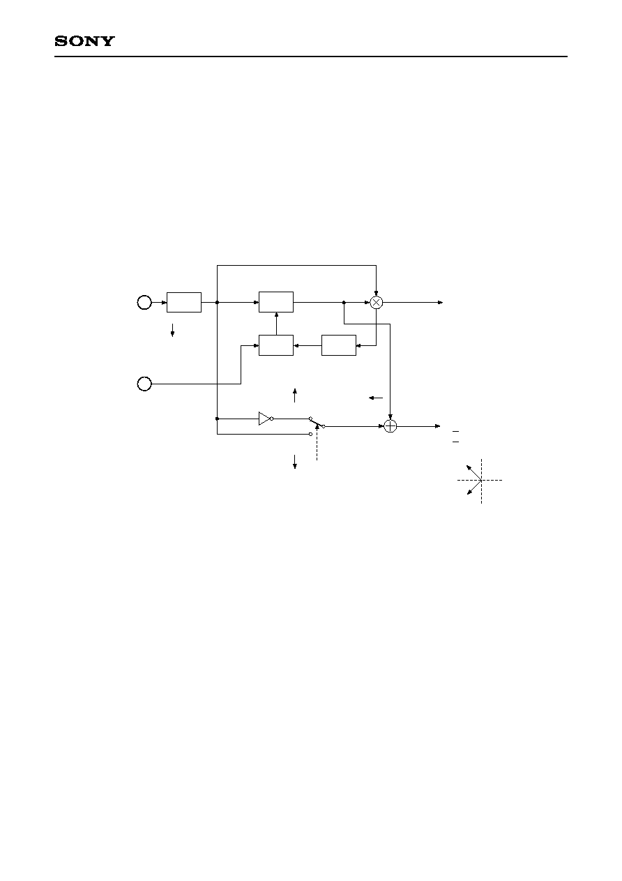
2. fsc ≠90∞ PLL,
◊
◊
2 and EX Burst Block
Fig. 2
The fsc ≠90∞ PLL consists of the ≠90∞ phase shifter, multiplier, LPF (low pass filter) 1 and V/I converter.
A signal delayed by 90∞ to the fsc is obtained in this PLL. By changing the DC voltage at Pin 23, the
amount of phase shift is varied. allowing adjustment of the phase of the EX burst and the duty (DC offset)
of the 2fsc. By applying 5V at Pin 23, the internally fixed phase shift is obtained. The 2fsc is produced
from the multiplier output (
◊
2 output).
The EX burst is produced by adding the fsc (or inverted fsc) to the fsc with 90∞ delay produced in the ≠90∞
PLL.
The fsc and the inverted fsc are switched in a period of 1/2f
H
, so the phase of the EX burst changes every
1H.
18
23
LIM
≠90
∞
V
I
LPF1
fsc
cos
t
2fsc
cos (2
t ≠ 90
∞
)
EX Burst
2 cos (
t ≠ 45
∞
)
2 cos (
t ≠ 135
∞
)
cos (
t ≠ 90
∞
)
cos (
t ≠ 180
∞
)
cos
t
1/2f
H
cos
t
ADJ

≠ 19 ≠
CXA1203M/N
Fig. 4
The above figure shows the relation between the phase of the burst signal, the phase of the fsc (fsc) and
the output at Pin 17 (SQ). As shown in the figure, the hysteresis angle is about 64∞. If the relation is as
shown in the figure below, the detector judges it as the correct sequence and set the output at Pin 17 to
HIGH.
Fig. 5
Therefore, the center phase of the burst signal (about the B-Y axis) should be ≠90∞ to the fsc.
3. SQ DET (Sequence Detector)
Fig. 3
The SQ DET detects the color alignment of the chrominance signal. The SQ PD is the phase detector which
operates for a burst period only. This detects the color alignment by comparing the phase of the fsc signal
inverted every 1H with the phase of the burst of the chrominance signal.
1/2f
H
fsc
SQ
P.D.
LPF3
Chrominance signal
Burst Flag Gate
17 SQ
≠180
∞
≠135
∞
≠90
∞
≠112
∞
≠48
∞
0
+48
∞
+90
∞
+135
∞
+180
∞
+112
∞
4V
Output at Pin 17
Phase of the burst signal
(on the bias of fsc and fsc)
0V
B-Y
fsc
≠135
∞
Burst
B-Y
fsc
+135
∞
Burst

≠ 20 ≠
CXA1203M/N
Fig. 7
The V-Invert circuit constructs the TH/DL APC loop that keep the phase difference between the burst of the
TH signal and the burst of the DL signal to be 90∞. This circuit detects the phase of the bursts of the TH and
DL signals and varies the delay time of the phase shifter
with reference to the error current of APC loop.
In PAL-M mode, the APC is applied to the fsc and the DL signal. Therefore, the input burst signal has a
phase of 90∞ to the fsc. The CONV1 is a multiplier to obtain the DL signal.
The Dummy supplies the same gain loss and the same phase delay as produced in CONV1 to the TH
signal so that there is no gain and phase difference between the TH signal and the DL signal.
The main SW outputs the TH or DL signal according to the TH/DL select signal (output at Pin 17). When a
BF Xch pulse is supplied (in JOG mode only), the EX burst is output.
4. V-Invert (V Axis Inversion Circuit)
For color alignment, the DL signal which is produced by inverting the chrominance signal (TH signal) about
the B-Y axis is necessary.
The V-Invert block produces the DL signal from the TH signal. Fig. 6 shows the principle of the V-Invert
block.
Fig. 6
Define the B-Y axis of the playback chrominance signal as cos
t and input the playback chrominance
signal and the 2fsc (cos 2
t) to the multiplier. By means of the frequency conversion of the 2fsc, the input
chrominance signal is inverted about the B-Y axis. The three fold frequency component (cos 3
t) is also
output, but this component is rejected by the BPF in a later stage.
Fig. 7 shows the actual V-Invert block.
◊
2
fsc (cos
t)
cos 2
t
DL: cos (
t
±
)
cos (3
t
±
)
TH: cos (
t
±
)
To
Y/C MIX BLOCK
Rejected by the BPF.
BPF
Playback chrominance
signal
cos (
t
±
)
V-I
LPF2
CONV1
Dummy
2fsc
BF Gate
EX Burst
fsc
PAL-M
PAL
TH/DL
BF Xch
Main
SW
SWD
1/2f
H
C OUT
TH
DL
15
Playback chrominance
signal

≠ 21 ≠
CXA1203M/N
Fig. 8
The AFC ID compares the C Sync frequency with the VCO frequency. When a frequency difference is
present, the AFC ID outputs an up or down error and roughly compensates the VCO frequency. In this
case, the AFC ID detects if the frequency difference continues for a period of 15H
◊
6 (5760µs), and AFC
ID error is available only when the frequency difference continues for that period.
The AFC ID also detects the existence of C Sync. When the C Sync is missing in various speed mode, the
AFC ID cuts off its output and maintains the state immediately before the output cutout.
The phase lock of the C Sync and VCO frequencies is carried out in the PLL loop composed of the S/H and
LPF circuits.
6. BELL and C-BELL Filters
The Bell Filter is applied to the SECAM color TV signal to suppress the level near the chrominance subcarrier
(F
OR
, F
OB
). In REC mode, the CXA1203 employs the BELL filter (having the inverted characteristics from the
Bell Filter) to obtain the chrominance subcarrier of the same amplitude at every hue. The output signal from
the BELL filter is sent to the record signal processing block of chrominance signal in the CXA1200.
In playback mode, the chrominance signal processed in the CXA1200 is input to the C-BELL (having the
same characteristics as the Bell Filter) filter of the CXA1203 to equalize the input signal with the SECAM
color TV signal. The output from the C-BELL Filter is mixed with the Y signal in the CXA1200 and sent to
the CXA1201. The typical input level of the BELL Filter is 32mVp-p, and that of the C-BELL Filter is 83mVp-p.
7. SECAM Detector Circuit
The SECAM detector circuit employed in the CXA1203 converts the chrominance subcarrier frequency
1
to
a voltage, and detects the color system by the voltage variation: PAL system if no voltage variation is
present, or SECAM system if the voltage varies every 1H. When the color alignment is carried out in
SECAM mode, the SECAM ACK output (Pin 3) is always set to HIGH by inputting the SECAM JUMP output
(Pin 7) to the DLDP (Pin 6).
1
PAL system:
color burst signal (4.43361875MHz)
SECAM system: line ID signal
F
OR
: 4.40625MHz
F
OB
: 4.25000MHz
5. f
H
PLL
HD
VCO
S/H
XSHP
C Sync
AFC
ID
LPF
1/2
1/2f
H
HD
SWD 1/2f
H
11
10

≠ 22 ≠
CXA1203M/N
Fig. 9. Application Circuit 1 (for PAL/SECAM mode)
5V
5V
5V
5V
5V
5V
BPF
1k
1k
1k
0.01
µ
20k
1k
20k
33k
2.2k
22k
1k
1k
1.5k
20k
100k
100k
100p
0.01
µ
0.01
µ
10p
1500p
5V
15k
390k
27k
33p
0.1
µ
110p
0.01
µ
0.01
µ
0.022
µ
39
820
100k
100k
1.2k
10
µ
1
µ
10
µ
3.3
µ
4.7
µ
1000p
4.7k
1k
10k
10k
JOG
REC/PB
BELL IN
SECAM IN
fsc IN
PB
CHROMA
OUT
PB
PB
REC (Se)
PB (PAL)
PB (Se)
REC
TH/DL
SWD
1/2FHM
TH/DL
(1/2FHTA)
PAL-M
BF
BF
PAL-M
PAL
CW
BF Xch
TH/DL
(1/2FHTA)
DL
TH
XPB
MASK 75 ≠ 1
MASK
75 ≠ 2
U ERRI
1/2FHM
PAL-M
TH/DL
XFHM
1/2FHM
1/2FHM
SA CONT
CLG PLS
CLP PLS
SWD
1/2FHT
1/2
FHT
SECAM
DETPLS
TEST
RST
Normal
SECAM
BELL IN
SECAM IN
H ID
Normal
1/2FHTAB
SWD1/2FHM
SWD1/2FHT
D ERRI
XSHP
MODE
C-BELL
BELL
AMP
≠90
∞
VCO
S/H
Peak
Hold
LPF2
S/H
75%
MASK2
75%
MASK1
EDGE
TRIG
EDGE
TRIG
Secam
P. D.
Jump
P. D.
HD
AFC
ID
D
V-I1
◊
2
SQ
P.D.
LPF1
LPF
CONT
Clamp
LPF1
FM
DEMOD
LPF3
CONV1
Dummy
LIM
LIM1
LIM2
V-I2
LPF2
SW
MAIN
SW
BF
Gen
75%
150%
D
1/2
D
BELL
FILTER
24
ADJ
23
BELL IN
22
MODE
21
SECAM
IN
20
DL GAIN
ADJ
19
fsc IN
18
SQ ID
17
DL APC
LPF
16
C OUT
15
IREF
14
VREG
13
V
CC
1
PB C IN
2
SECAM
ACK
3
1/2FHMP
4
75% C
5
DLDP
6
SECAM
JUMP
7
SECAM
LPF
8
AFC
LPF
9
HD
10
C Sync
11
GND
12
PB CHROMA IN
SECAM ACK
C Sync
Vcc
20k
Application circuits shown are typical examples illustrating the operation of the devices. Sony cannot assume responsibility for
any problems arising out of the use of these circuits or for any infringement of third party patent and other right due to same.

≠ 23 ≠
CXA1203M/N
Fig. 10. Application Circuit 2 (for PAL mode only)
5V
5V
5V
5V
5V
BPF
1k
1k
1k
0.01
µ
20k
1k
20k
33k
2.2k
22k
1k
1k
1.5k
20k
100k
100k
100p
0.01
µ
0.01
µ
10p
1500p
110p
0.01
µ
0.01
µ
20k
100k
100k
10
µ
1
µ
10
µ
4.7
µ
1000p
4.7k
10k
10k
JOG
REC/PB
fsc IN
PB
CHROMA
OUT
20k
PB
PB
REC (Se)
PB (PAL)
PB (Se)
REC
TH/DL
SWD
1/2FHM
TH/DL
(1/2FHTA)
PAL-M
BF
BF
PAL-M
PAL
CW
BF Xch
TH/DL
(1/2FHTA)
DL
TH
XPB
MASK 75 ≠ 1
MASK
75 ≠ 2
U ERRI
1/2FHM
PAL-M
TH/DL
XFHM
1/2FHM
1/2FHM
SA CONT
CLG PLS
CLP PLS
SWD
1/2FHT
1/2
FHT
SECAM
DETPLS
TEST
RST
Normal
SECAM
BELL IN
SECAM IN
H ID
Normal
1/2FHTAB
SWD1/2FHM
SWD1/2FHT
D ERRI
XSHP
MODE
C-BELL
BELL
AMP
≠90
∞
VCO
S/H
Peak
Hold
LPF2
S/H
75%
MASK2
75%
MASK1
EDGE
TRIG
EDGE
TRIG
Secam
P. D.
Jump
P. D.
HD
AFC
ID
D
V-I1
◊
2
SQ
P.D.
LPF1
LPF
CONT
Clamp
LPF1
FM
DEMOD
LPF3
CONV1
Dummy
LIM
LIM1
LIM2
V-I2
LPF2
SW
MAIN
SW
BF
Gen
75%
150%
D
1/2
D
BELL
FILTER
24
ADJ
23
BELL IN
22
MODE
21
SECAM
IN
20
DL GAIN
ADJ
19
fsc IN
18
SQ ID
17
DL APC
LPF
16
C OUT
15
IREF
14
VREG
13
V
CC
1
PB C IN
2
SECAM
ACK
3
1/2FHMP
4
75% C
5
DLDP
6
SECAM
JUMP
7
SECAM
LPF
8
AFC
LPF
9
HD
10
C Sync
11
GND
12
PB CHROMA IN
C Sync
Vcc
Application circuits shown are typical examples illustrating the operation of the devices. Sony cannot assume responsibility for
any problems arising out of the use of these circuits or for any infringement of third party patent and other right due to same.

≠ 24 ≠
CXA1203M/N
Notes on Use
1. Phase Adjustment in PAL Playback Mode
The phase of the EX burst signal can be adjusted with the phase of the input fsc (chrominance subcarrier).
The phase of the DL signal can be adjusted by applying a current to Pin 16.
Adjust the phase of the fsc so that the phase of the EX burst signal in JOG playback mode matches the
phase of the color burst signal in normal playback mode at the PB CHROMA output (Pin 15).
Then, adjust the current to be applied to Pin 16 so that the DL signal becomes symmetrical to the TH signal
about the B-Y axis.
2. PAL-M Mode
Fig. 11
Input an NTSC signal to Pin 2, the fsc signal (3.58MHz) to Pin 18 and the C Sync signal (15.75MHz) to Pin 11.
Then the PAL-M playback signal is obtained at PB CHROMA output (Pin 15).
To adjust the phase, first input a burst signal with the same phase as the B-Y axis, and adjust the phase of
the fsc to be input so that the phase of the TH signal matches the center phase of the EX burst at Pin 15.
Then adjust the current to be applied to Pin 16 so that the phase of the DL signal matches the center phase
of the EX burst. In PAL-M mode, Pin 17 (SQ ID) should be fixed to "L".
3. PAL Only Mode
In PAL only mode, a part of the SECAM detector block is turned off by fixing Pin 22 (BELL IN) to "H". This
reduces the current consumption to 1.2mA. The connections for other pins are the same as shown in "Fig. 10
Application Circuit 2 (for PAL mode only)".
B-Y
R-Y
fsc
TH and DL
signals
EX burst
B-Y
R-Y
Output
Input
fsc
Input signal
≠ 25 ≠
CXA1203M/N
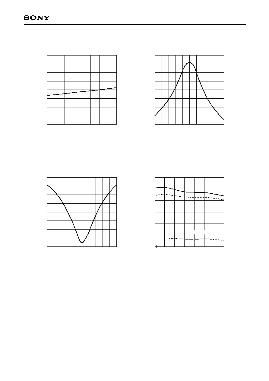
Example of Representative Characteristics
VREG supply voltage characteristic
Vcc (Pin 1) [V]
4.50
4.21
4.22
4.23
4.24
4.25
4.75
5.00
5.25
5.50
VREG (Pin 13) [V]
TH/DL/EX burst output level vs. Ambient temperature
Ta ≠ Ambient temperature [
∞
C]
≠10
100
120
140
160
0
25
50
75
Output level [mVp-p]
BELL Filter characteristic
f ≠ Frequency [MHz]
3.786
0
2.0
4.0
6.0
8.0
10.0
12.0
14.0
16.0
4.286
4.786
Vcc = 5.0V
SECAM/REC mode
Input level: 32mVp-p (BELL IN)
Output: C OUT (Pin 15)
Gain [dB]
C-BELL Filter characteristic
f ≠ Frequency [MHz]
3.786
0
2.0
4.0
6.0
8.0
10.0
12.0
14.0
16.0
4.286
4.786
Vcc = 5.0V
SECAM/PB mode
Input level: 83mVp-p (BELL IN)
Output: C OUT (Pin 15)
Vcc = 5.0V
PAL/PB mode
Input level: 150mVp-p (PB C IN)
fsc: 350mVp-p
Output: 4.43MHz BPF OUT
(The output level is the average during 2H.)
Gain [dB]
DL
TH
EX burst

≠ 26 ≠
CXA1203M/N
Phases of the HD and EX burst vs. Ambient temperature
Relation of the phase of each pulse to the C Sync signal
Ta ≠ Ambient temperature [
∞
C]
0
0
1.0
2.0
3.0
5.0
4.0
25
50
75
Time [
µ
s]
SQ DET input/output vs. Ambient temperature
Ta ≠ Ambient temperature [
∞
C]
40
60
80
100
120
0
25
50
75
Phase of the input signal [deg]
TH/DL/EX burst phases vs. Ambient temperature
Ta ≠ Ambient temperature [
∞
C]
≠10
92
98
96
94
106
104
102
100
112
110
108
0
25
50
75
Phase [deg]
Vcc = 5.0V
PAL/PB mode
Input level: 150mVp-p
(PB C IN)
fsc: 350mVp-p
Output: C OUT (Pin 15)
DL
TH
EX burst
Vcc = 5.0V
PAL/RESET mode
Input level: 150mVp-p
(PB C IN)
fsc: 350mVp-p
Output: SQ ID (Pin 17)
Output at Pin 17
L
H
Output at Pin 17
H
L
The phase is the absolute value
determined by measuring the
center angle of the TL, DL or EX
burst during 2H with reference to
the fsc (at Pin 18).
The phase of the input
signal is the absolute value
of the phase delay to the
fsc. This is determined by
delaying the phase of the
input signal to the fsc and
measuring the phase delay
when the output changes.
A
C
B
D
A
B
C
D
C Sync
(Pin 11)
HD
(Pin 10)
EX burst
(Pin 15)

≠ 27 ≠
CXA1203M/N
CXA1203M
Kokubu Ass'y
SONY CODE
EIAJ CODE
JEDEC CODE
M
PACKAGE STRUCTURE
MOLDING COMPOUND
LEAD TREATMENT
LEAD MATERIAL
PACKAGE MASS
EPOXY RESIN
SOLDER PLATING
42/COPPER ALLOY
24PIN SOP (PLASTIC)
15.0 ≠ 0.1
+ 0.4
1
12
13
24
0.45
±
0.1
5.3
≠
0.1
+ 0.3
7.9
±
0.4
0.2 ≠ 0.05
+ 0.1
0.5
±
0.2
0.1 ≠ 0.05
+ 0.2
0.15
1.85 ≠ 0.15
+ 0.4
6.9
0.24
SOP-24P-L01
SOP024-P-0300
0.3g
1.27
LEAD PLATING SPECIFICATIONS
ITEM
LEAD MATERIAL
COPPER ALLOY
SOLDER COMPOSITION
Sn-Bi Bi:1-4wt%
PLATING THICKNESS
5-18
µ
m
SPEC.
Package Outline
Unit: mm

≠ 28 ≠
CXA1203M/N
CXA1203N
Sony Corporation
SONY CODE
EIAJ CODE
JEDEC CODE
SSOP-24P-L01
P-SSOP24-7.8x5.6-0.65
PACKAGE MATERIAL
LEAD TREATMENT
LEAD MATERIAL
PACKAGE MASS
EPOXY RESIN
PALLADIUM PLATING
COPPER ALLOY
PACKAGE STRUCTURE
0.1g
24PIN SSOP (PLASTIC)
0.1
±
0.1
0
∞
to 10
∞
0.5
±
0.2
DETAIL A
5.6
±
0.1
24
7.8
±
0.1
13
0.65
12
1
7.6
±
0.2
0.1
1.25 ≠ 0.1
+ 0.2
A
0.13 M
NOTE: Dimension "
" does not include mold protrusion.
0.15
≠
0.01
DETAIL B : PALLADIUM
+ 0.03
b=0.22
±
0.03
B
b
Package Outline
Unit: mm