 | –≠–ª–µ–∫—Ç—Ä–æ–Ω–Ω—ã–π –∫–æ–º–ø–æ–Ω–µ–Ω—Ç: CXA1211 | –°–∫–∞—á–∞—Ç—å:  PDF PDF  ZIP ZIP |
Electronic Volume
Description
The CXA1211M is a wide band general-purpose
VCA. This bipolar IC incorporates 2 chnannels.
Features
∑ Wide band frequency characteristics:
100kHz to 20MHz (≠0.5dB)
∑ Wide dynamic range
∑ Low noise, low distortion
∑ Low power consumption
Applications
Video signals and other wide band VCA
Operating Conditions
Supply voltage
V
CC
4.50 to 5.50
V
Absolute Maximum Ratings
∑ Supply voltage
V
CC
14
V
∑ Operating temperature
Topr
≠20 to +75
∞C
∑ Storage temperature
Tstg
≠65 to +150
∞C
∑ Allowable power dissipation
P
D
510
mW
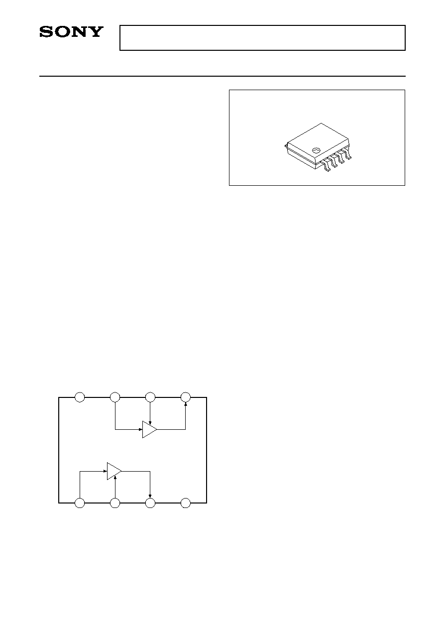
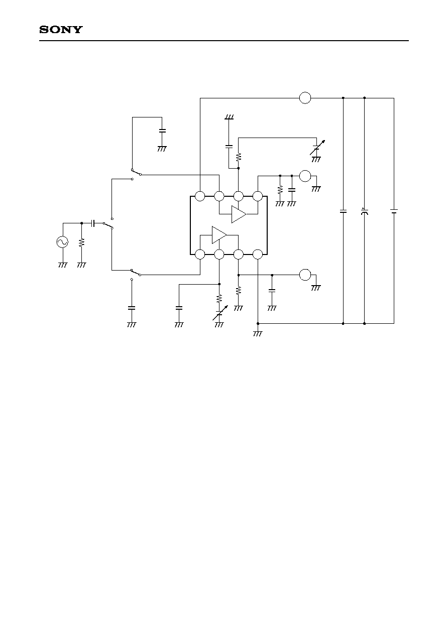
Block Diagram and Pin Configuration
≠ 1 ≠
E90534D8X
Sony reserves the right to change products and specifications without prior notice. This information does not convey any license by
any implication or otherwise under any patents or other right. Application circuits shown, if any, are typical examples illustrating the
operation of the devices. Sony cannot assume responsibility for any problems arising out of the use of these circuits.
CXA1211M
8 pin SOP (Plastic)
2
3
4
1
5
6
7
8
IN1
CONT1
OUT1
GND
V
CC
IN2
CONT2
OUT2
VCA2
VCA1
≠ 2 ≠
CXA1211M
Pin Description
Pin
No.
1
IN1
2.5V 1.0Vp-p
40k
Signal input pin
(CH1)
Symbol
Voltage
DC
AC
I/O
resistance
Equivalent circuit
Description
V
CC
GND
1
40k
3k
2
CONT1
2.7V
--
Input pin of gain control signal
(CH1).
At "Low" power save is
possible.
Low: 1V and below
V
CC
GND
24k
2
5k
100µ
1µ 100µ
3
OUT1
1.9V 1.0Vp-p
Signal output pin
(CH1)
3
129
V
CC
GND
1m
5
OUT2
1.9V 1.0Vp-p
Signal output pin
(CH2)
129
V
CC
GND
1m
5
4
GND
0V
--
--
--
GND pin
External input
≠ 3 ≠
CXA1211M
Pin
No.
6
CONT2
2.7V
--
Input pin of gain control signal
(CH2).
At "Low" power save is
possible.
Low: 1V and below
Symbol
Voltage
DC
AC
I/O
resistance
Equivalent circuit
Description
V
CC
GND
24k
5k
100µ
1µ 100µ
6
7
IN2
2.5V 1.0Vp-p
40k
Signal input pin
(CH2)
V
CC
GND
40k
3k
7
8
V
CC
5V
--
--
--
V
CC
pin
External input

≠ 4 ≠
CXA1211M
Notes on Operation
Do not fail to take the following precautions upon usage of the CXA1211M.
1. Countermeasure to cross talk between channels
Fix a bypass capacitor to Pins CONT1 and CONT2 that control the amplifier gain. When the impedance of
the control voltage source is visible, depending on the package volume and others, cross talk between
channels is easily generated.
2. Input signal dynamic range
The input dynamic range is at a max of 1.4Vp-p. When the input signal exceeds 1.4Vp-p, the waveform may
be clipped and deformed.
≠ 5 ≠
CXA1211M
Electrical Characteristics
(Ta = 25∞C, V
CC
= 5.0V, See Electrical Characteristics Test Circuit.)
Item
Current
consumption
1-ch
Both-ch
CH1
CH2
CH1
CH2
CH1
CH2
CH1
CH2
CH1
CH2
I
1CH
I
2CH
G
1MAX
G
2MAX
G
1MIN
G
2MIN
V
F1
V
F2
D
1CH
D
2CH
N
1CH
N
2CH
1
7
500
mVp-p
500
mVp-p
500
mVp-p
1.0
Vp-p
0.5
Vp-p
300
kHz
300
kHz
300k
to
20M
5.0
MHz
100k
to
4.2M
3.0
4.5
2.0
≠7.0
≠1.0
5.0
7.5
4.0
≠5.0
≠40
61
7.0
12
6.0
≠3.0
+1.3
dB
mA
dB
dB
dB
dB
5.0
2.87
0
1.8
2.87
1.8
0, 1
7
0
0, 1
7
0, 1
7
0, 1
7
0, 1
7
3
5
A8
When only 1ch is
used, ch used is set
to 2.87V.
3
5
3
5
3
Adjust CONT to
obtain 1.0Vp-p at
output
Test at no signal
conditon
20MHz level
300kHz level
5
3
5
1
7
1
7
1
7
1
7
Max. gain
Min. gain
Frequency
characteristics
Distortion 1
S/N
Symbol
Test conditions
Test method
Min. Typ. Max. Unit
Test point
Input conditions
IN Level Freq
CONT
voltage
(V)
SW set
to ON
≠ 6 ≠
CXA1211M
Electrical Characteristics Test Circuit
2
3
4
1
5
6
7
8
I
N
1
C
O
N
T
1
O
U
T
1
G
N
D
V
C
C
I
N
2
C
O
N
T
2
O
U
T
2
VCA2
VCA1
V5
10k
10P
51k
V3
0.01µ
3300P
47µ
V1
10k
10P
V3
51k
V2
0.01µ
0.1µ
SW7
ON
OFF
SW1
ON
OFF
0.1µ
SW0
ON
OFF
0.1µ
51
S.G.
A8
≠ 7 ≠
CXA1211M
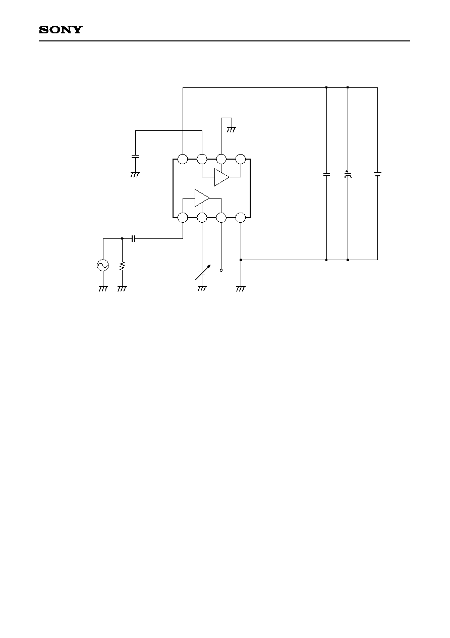
Application Circuit
2
3
4
1
5
6
7
8
GND
V
CC
VCA2
VCA1
3300P
47µ
5V
CONT
0.1µ
0.1µ
51
S.G.
When VCA2 is not in use
Application circuits shown are typical examples illustrating the operation of the devices. Sony cannot assume responsibility for
any problems arising out of the use of these circuits or for any infringement of third party patent and other right due to same.
≠ 8 ≠
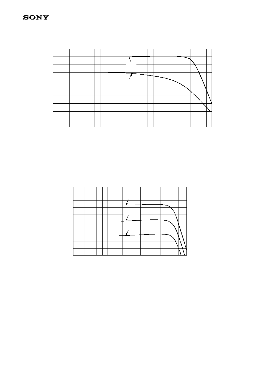
CXA1211M
0.1
1
10
100
Frequency [MHz]
150∞
100∞
50∞
0∞
≠50∞
≠100∞
≠150∞
≠200∞
≠250∞
≠300∞
≠350∞
P
h
a
s
e
[
d
e
g
r
e
e
]
Frequency characteristics 1 (When Gain = 0dB)
2.0
0
≠2
≠4
≠6
≠8
≠10
≠12
≠14
≠16
≠18
G
a
i
n
[
d
B
]
0.1
1
10
100
Frequency [MHz]
+10
8
6
4
2
0
≠2
≠4
≠6
≠8
≠10
G
a
i
n
[
d
B
]
Frequency characteristics 2 (MAX Gain, MIN Gain)
Gain
Phase
MAX
NORMAL
MIN

≠ 9 ≠
CXA1211M
2.0
CONT [V]
Gain vs. CONT voltage characteristics
≠4
G
a
i
n
[
d
B
]
3.0
4.0
5.0
≠3
≠2
≠1
0
1
2
3
4
5
Room temperature
V
CC
= 5.0V
≠20
Temperature [∞C]
Gain vs. Temperature characteristics
≠0.5
G
a
i
n
[
d
B
]
0
40
100
≠0.4
≠0.3
≠0.2
≠0.1
0.0
0.1
0.2
0.3
0.4
20
60
80
V
CC
= 5.0V
f = 300kHz
Adjust to 0dB at 20∞C
≠ 10 ≠
CXA1211M
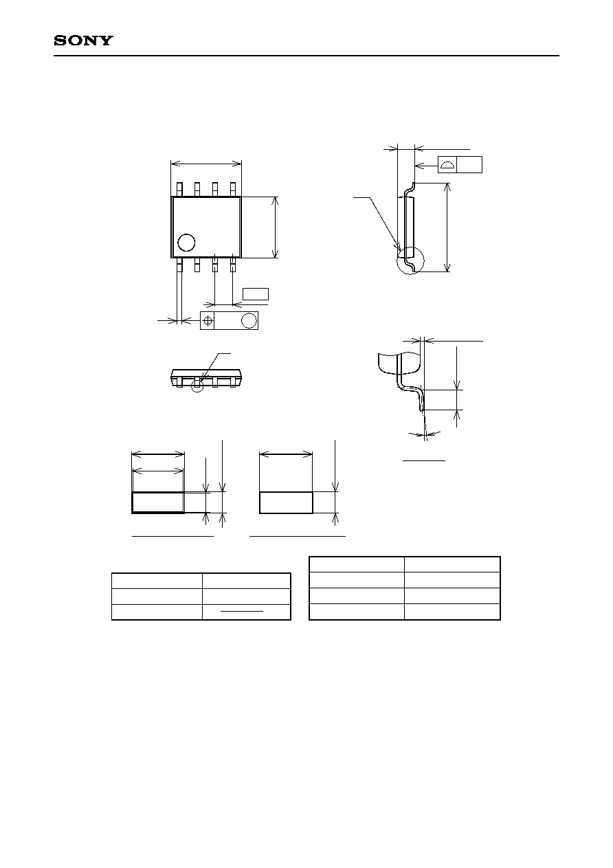
Package Outline
Unit: mm
PACKAGE STRUCTURE
PACKAGE MATERIAL
LEAD TREATMENT
LEAD MATERIAL
PACKAGE MASS
EPOXY RESIN
SOLDER/PALLADIUM
42/COPPER ALLOY
0.1g
SOP-8P-L03
SOP008-P-0225
8PIN SOP (PLASTIC)
SONY CODE
EIAJ CODE
JEDEC CODE
0∞ to 10∞
0.1 ≠ 0.1
+ 0.15
0
.
5
±
0
.
2
DETAILA
8
5
1
4
4
.
4
≠
0
.
1
+
0
.
3
1.27
1.25 ≠ 0.15
+ 0.4
6
.
4
±
0
.
4
A
5.0 ≠ 0.1
+ 0.4
0.10
PLATING
M
0.24
b
B
(
0
.
1
5
)
0
.
1
5
≠
0
.
0
5
(0.4)
b = 0.4 ≠ 0.05
DETAIL B : SOLDER
0
.
1
5
≠
0
.
0
1
b = 0.4 ± 0.03
DETAIL B : PALLADIUM
+
0
.
0
3
+ 0.1
+
0
.
1
NOTE : PALLADIUM PLATING
This product uses S-PdPPF (Sony Spec.-Palladium Pre-Plated Lead Frame).