 | –≠–ª–µ–∫—Ç—Ä–æ–Ω–Ω—ã–π –∫–æ–º–ø–æ–Ω–µ–Ω—Ç: CXA1704R | –°–∫–∞—á–∞—Ç—å:  PDF PDF  ZIP ZIP |

--1--
E93860A66-TE
Sony reserves the right to change products and specifications without prior notice. This information does not convey any license by
any implication or otherwise under any patents or other right. Application circuits shown, if any, are typical examples illustrating the
operation of the devices. Sony cannot assume responsibility for any problems arising out of the use of these circuits.
Absolute Maximum Ratings (Ta=25∞C)
∑ Supply voltage
V
CC
7
V
∑ Operating temperature
Topr
≠10 to +75
∞C
∑ Storage temperature
Tstg
≠65 to +150
∞C
∑ Allowable power dissipation
P
D
1100
mW
(when board is mounted)
Operating Conditions
Supply voltage
V
CC
4.75
+0.5
V
≠0.25
Description
The CXA1704R is a bipolar IC designed as a
recording/playback amplifier for Hi8-compatible
VCRs.
Features
O Recording system
∑ Feedback damping provided in the recording
amplifier and its EVR control function facilitate
circuit board design.
∑ Y, chroma, and low-band level adjustment
functions
∑ Ramp circuit
O Playback system
∑ Feedback damping provided in the playback
amplifier facilitates circuit board design.
∑ Middle-frequency tuner on chip; EVR permits
independent adjustment of f
0
, Q and boost
∑ RF AGC and dropout detection circuit
Structure
Bipolar silicon monolithic IC
2-channel REC/PB Amplifier for 8mm VCR
48 pin LQFP (Plastic)
CXA1704R
--2--
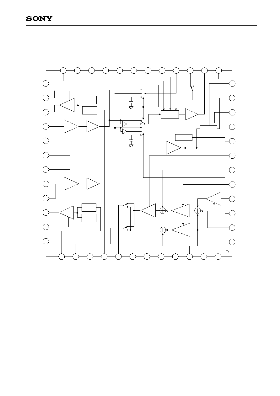
CXA1704R
Block Diagram and Pin Configuration
HEAD
40dB
15dB
HEAD
40dB
15dB
REC
22
21
20
19
18
17
16
15
14
13
12
1
2
3
4
5
6
7
8
9
10
11
23
24
25
26
27
28
29
30
31
32
33
34
35
36
37
38
39
40
41
42
43
44
45
46
47
48
VCC
T1
RFSWP
T2
T3
MTQ
RP_PB
MTF0
PCMOUT
MTG2
MTOUT
MTG1
VCC1
REC1CONT
REC1OUT
PB1IN
GND1
PBDUMP1
PBDUMP2
GND2
PB2IN
REC2OUT
REC2CONT
VCC2
REC
RAMP
GEN
V/I
V/I
RAMP
GEN
1CH(0dB)
1CH(6dB)
2CH(0dB)
2CH(6dB)
MUTE
1CH
2CH
MUTE
PCMSW
VIDEOSW
12dB
MTGSW
RF
AGC
DOCDET
AGCDET
CGCA
LOWGCA
LOWGCA
YGCA
VPSW1
VPSW2
1
1
1
1
1
1
2
REC2IN
VPSW2OUT
VREG
REC1IN
VPSW1OUT
GND
IR1
IR
VG2
PCMIN
PCMREC
ATFIN
CCONT
AFMIN
XGAIN
CIN
LOWLEVEL
YIN
YLEVEL
RFAGCOUT
RFAGCTC
RFAGCIN
DOCDET
DOP
M∑T
≠6dB
VIDEO
PCM
VIDEO
PCM
--3--
CXA1704R
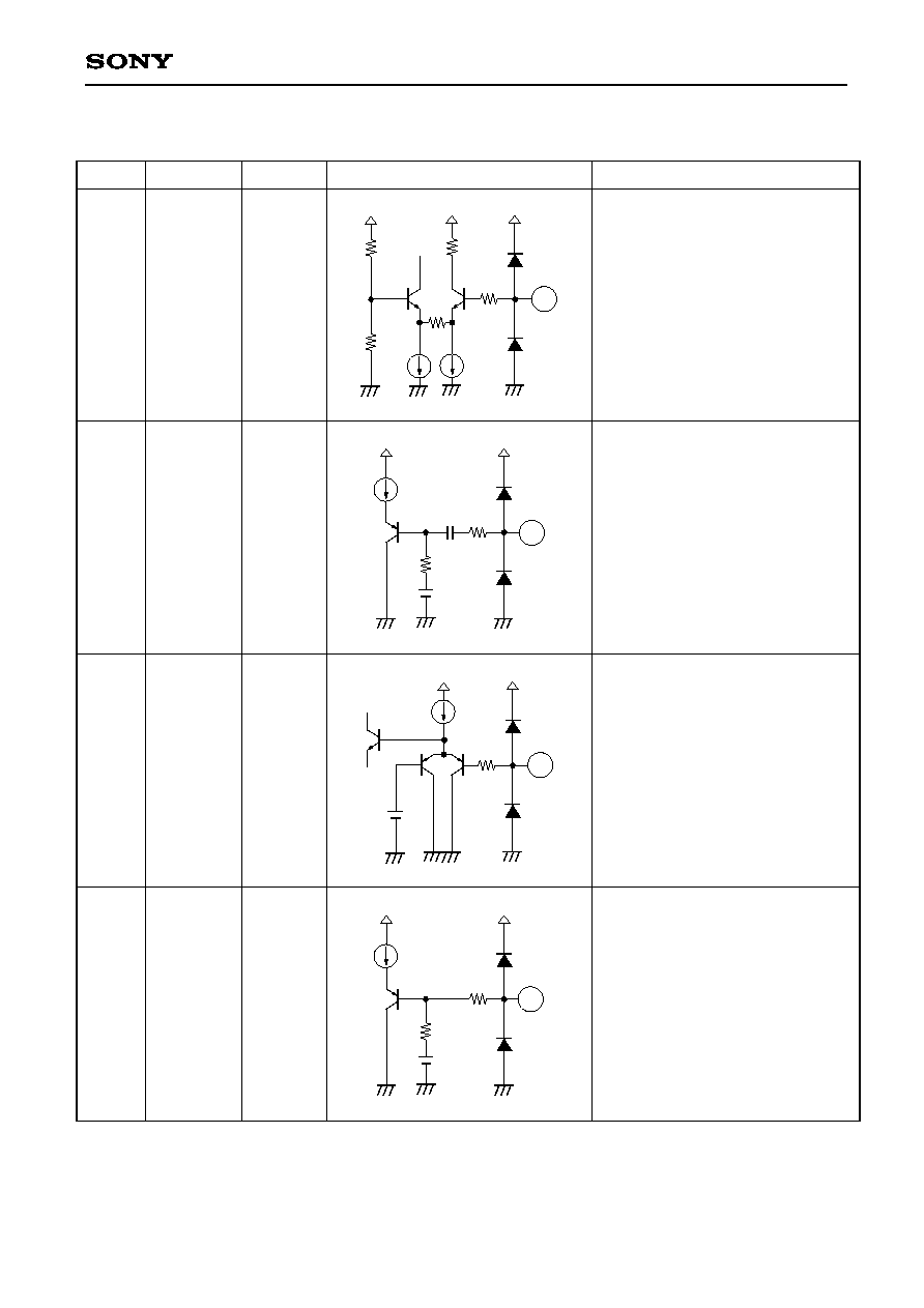
Pin Description
1
CCONT
--
2
AFMIN
--
3
XGAIN
--
4
CIN
2.4 V
1
143
270
25k
90µ
90µ
32.5k
67.5k
143
60µ
2
50k
20p
143
35µ
3
143
70µ
50k
4
EVR adjustment of recording
chroma level.
Gain is small when the applied
voltage is large.
Recording AFM input.
DC is cut off by internal capacitor.
Input level is 125 mVp-p (typ.).
When not used, connect this pin to
Vcc.
VIDEO SW gain switch.
Low : 6 dB
High : 0 dB
Recording chroma input.
Input the signal with capacitor
coupling.
Input level is 300 mVp-p (typ.).
Pin No.
Symbol
Pin voltage
Equivalent circuit
Description
--4--
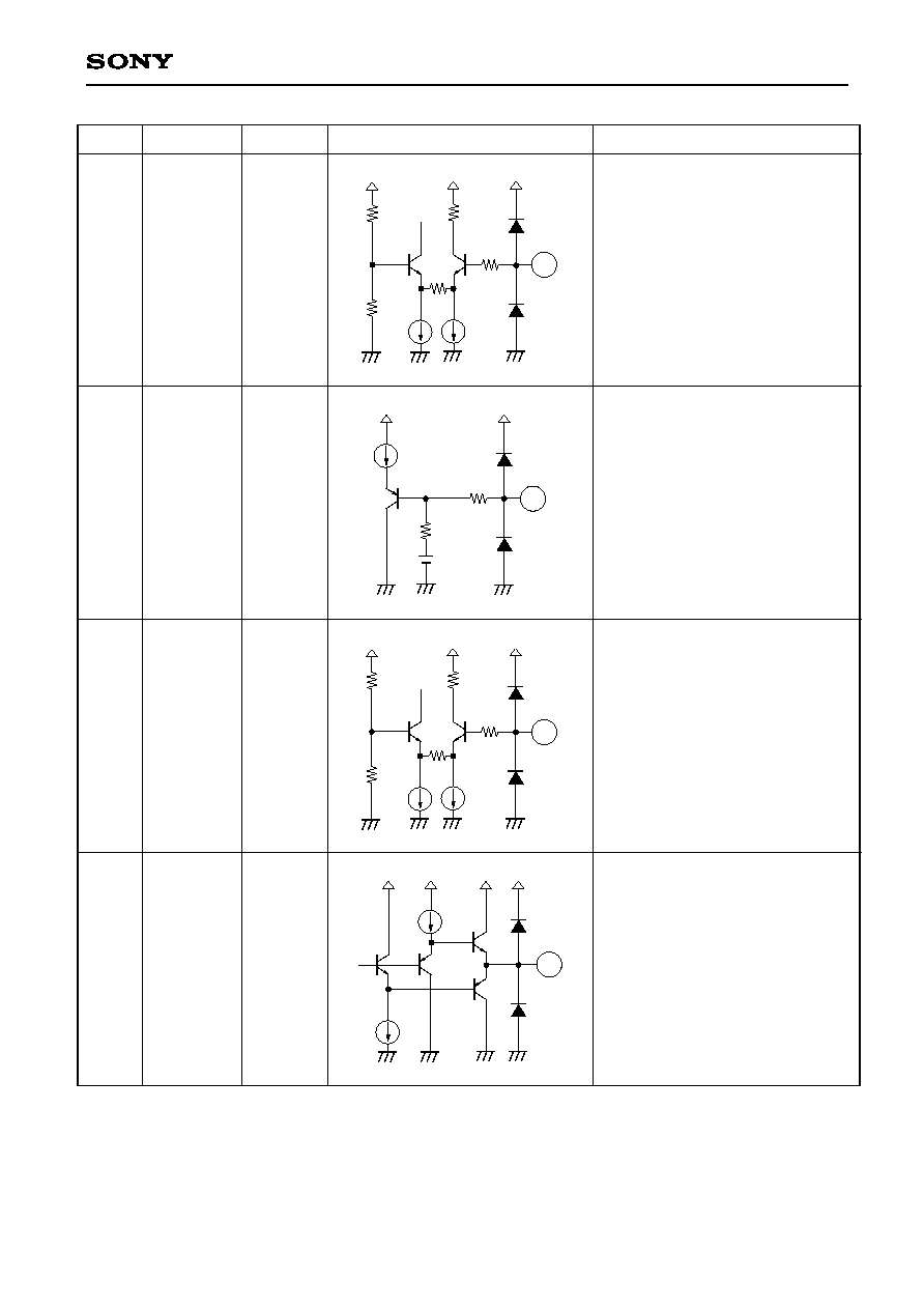
CXA1704R
5
LOW LEVEL
--
6
YIN
2.4 V
7
YLEVEL
--
8
RFAGCOUT
2.8 V
EVR adjustment of recording RF
signal level.
Gain is small when the applied
voltage is large.
Adjusts both the VIDEO path and
the PCM path simultaneously.
VIDEO path:
Adjustment of C + AFM + ATF
PCM path: Adjustment of ATF
Recording Y signal input.
Input the signal with capacitor
coupling.
Input level is 500 mVp-p (typ.).
EVR adjustment of recording Y
signal level.
The Y LEVEL is small when the
applied voltage is large.
Playback Y signal output.
Output level is 380 mVp-p (typ.).
Pin No.
Symbol
Pin voltage
Equivalent circuit
Description
143
270
21k
90µ
90µ
33.5k
66.5k
5
143
40µ
50k
6
143
270
23k
90µ
90µ
32.5k
67.5k
7
600µ
40µ
8

--5--
CXA1704R
9
RFAGCTC
--
10
RFAGCIN
--
11
DOCDET
2.5 V
12
DOP
H: 3.1 V
L: 0 V
143
50µ
79k
47k
11
46.5k
72k
2.4k
150
64k
100k
12
RF AGC time constant.
RF AGC input of playback Y level.
The playback video signal output
from Pin 14 (MTOUT) passes
through an external ATF TRAP,
AFM TRAP, and C TRAP, and is
then input to Pin 10 (RFAGCIN)
again.
DC is cut off by internal capacitor.
When not used, connect this pin to
Vcc.
Determines the dropout detection
level.
Dropout detection signal output.
Goes high when a dropout is
detected.
Pin No.
Symbol
Pin voltage
Equivalent circuit
Description
25µ
9
143
25µ
25µ
143
50µ
50k
13p
10