 | –≠–ª–µ–∫—Ç—Ä–æ–Ω–Ω—ã–π –∫–æ–º–ø–æ–Ω–µ–Ω—Ç: CXA1810AR | –°–∫–∞—á–∞—Ç—å:  PDF PDF  ZIP ZIP |

--1--
E94X24-TE
Sony reserves the right to change products and specifications without prior notice. This information does not convey any license by
any implication or otherwise under any patents or other right. Application circuits shown, if any, are typical examples illustrating the
operation of the devices. Sony cannot assume responsibility for any problems arising out of the use of these circuits.
Absolute Maximum Ratings (Ta=25 ∞C)
∑ Supply voltage
V
CC
7
V
∑ Operating temperature Topr
≠10 to +75
∞C
∑ Storage temperature
Tstg
≠65 to +150
∞C
∑ allowable power dissipation
(when mounted on board)
P
D
CXA1810AQ 1050 mW
CXA1810AR 1010 mW
Operating Condition
Supply voltage
V
CC
4.75+0.5 to 4.75≠0.25
V
Description
The CXA1810AQ/AR is an IC designed for 8mm
VCR Y/C main signal processing for consumer use.
Equipped with many built-in filters, the
CXA1810AQ/AR is a one-chip main signal
processing system that greatly reduces the number
of external components.
Features
∑ Built-in auto-adjusting filters
∑ Supports Hi-8 video.
∑ Supports camera recording.
∑ Supports power saving mode.
140 mW for composite signal input
250 mW for separate signal input
∑ Supports electronic volume (EVR) control.
∑ Supports BUS LINE.
∑ Supports NTSC/PAL.
Functions
2-input INPUT SELECT, VIDEO AGC, DDS (Y
signal superimposition), synchronous separation, 75
VIDEO OUT DRIVE, Y/C mixing, Y/C separation
comb filter, Y/C cross talk elimination, playback
chroma feedback comb, Y dropout compensation,
Yd playback switching, Y signal H correlation
detection, Y pre-emphasis/de-emphasis, white/dark
clipping, clipping compensation, MOD/DEMOD,
HHS/HHS cancel, ACC, chroma emphasis/de-
emphasis, burst emphasis/de-emphasis, XO/VXO,
APC, AFC, APC ID, AFC ID, burst ID, ACK, APC
compensation, HHK, PI/PS, frequency conversion
system, PB C BPF, REC C LPF, PB C LPF,
CARRIER BPF, 4.1 V regulator
Structure
Bipolar silicon monolithic IC
Luminance and Color Signal Processing for 8mm VCR
CXA1810AQ
CXA1810AR
64 pin QFP (Plastic)
64 pin LQFP (Plastic)
CXA1810AQ/AR
--2--
CXA1810AQ/AR
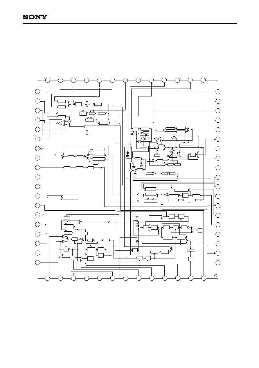
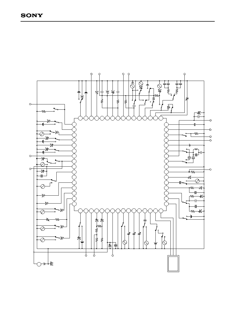
Block Diagram and Pin Configuration
(CXA1810AQ)
S∑REC
+ACK∑REC
S∑REC
+ACK∑REC
BUS DECODER
HHK
AFC DET
AFC ID
APC ID
1/8
APC
DET
ACK BID
DET
ACK
CONT
ACK
BID
FF
f
o
AUTO
CAR
CONV
1/N
CAR
BPF
VXO
XO
VCO
BF
CXA1810AQ
SWP
CAR. CONT
DEV. CONT
SMEAR. CONT
HHS
LPF
DEMOD
LIM
LIM
MOD
SYNC SEP
CLAMP
CLAMP
CLAMP
CLAMP
VIDEO
AGC
AGC DET
VD/HD
INSERT
Y MUTE
DDS
DOC TRAP
VCA 1
CLAMP 1
SYNC
ATT
ATT
BPF
ATT
LIM
TRAP
EQ
EQ
f
s c
TRAP
VCA 2
CLAMP 2
CLAMP 3
Sharpness
HPF
Y CORRE DET
NOISE CANCELLER
W/D CLIP
SMEAR COMP
Y EMPH
Y DE EMPH
CLAMP
HARD
CLIP
HHS CANCEL
SWP
CLIP COMP
PI
PS
REC C
LPF
REC
CONV
BURST
EMPH
BURST
DEEMPH
CROMA
EMPH
ACC
AMP
CAR
INV
PB C
LPF
PB
CONV
PB C
BPF
ACC
CONT
ACC
DET
CROMA
DEEMPH
SWP
ACK
SW
SWP
ACK
SW
C MUTE
INSEL
AGC OFF
ON
PB
S∑REC+PB
REC
TEST2
REC
TEST2
TEST1
REC
PB
REC
PB
CAM REC
TEST1
REC
PB
TEST1
REC
PB
REC
PB
C SEL
REC
PB
REC
PB
S∑REC
PB
EDIT
PB∑ACK
NO CORR
S∑REC
W∑PB
PB
W∑PB
DOP
W∑PB
Yd PB
PB
Yd PB
PB
REC
REC
W∑PB
PB
REC
SHP
THROU
E
PB+REC CORR
REC∑(S+443+EDIT+NO CORR)
+
+
+
--
+
≠
+
≠
+ +
+ +
+
≠
≠
+
+
+ +
+
1
2
3
4
5
6
7
8
9
10
11
12
13
14
15
16
17
18
19
20
21
22
23
24
25
26
27
28
29
30
31
32
33
34
35
36
37
38
39
40
41
42
43
44
45
46
47
48
49
50
51
52
53
54
55
56
57
58
59
60
61
62
63
64
CLAMP
TC1
Y OUT
V OUT
GND
VIDEO
OUT
INV IN
RF/V
V
CC
Y RF
OUT
RF GND
Y RF IN
SMEAR
CONT
DEV
CONT
CARR
CONT
PB C IN
SWP
CS
SI
CK
D. O.
PULSE
APC
FL
Y
I
N
R
E
C
L
/
J
V
D
V
I
N
1
A
G
C
T
C
1
V
I
N
2
W
D
C
D
D
S
/
M
A
S
K
V
C
C
C
O
M
P
S
Y
N
C
D
L
I
N
1
A
G
C
T
C
2
D
L
O
U
T
1
C
L
A
M
P
T
C
2
DL OUT2
CLAMP
TC3
DL IN2
AGC TC3
COMB
ADJ
LIM C
Y COMB
OUT
C TRAP
VG1
DEEMPH
IN
COMP TC
REC
C OUT
DEMOD
OUT
NC TC IN
EMPH IN
SUB
EMPH TC
MAIN
EMPH TC
MAIN
EMPH OUT
C EMPH
CONT
A
F
C
F
L
E
X
T
C
I
N
D
C
F
B
I
R
E
F
G
N
D
X
T
A
L
I
N
V
R
E
G
X
T
A
L
O
U
T
C
A
M
F
S
C
S
H
P
F
S
C
O
U
T
B
F
V
C
O
C
O
U
T
C
I
N
90∞
SHIFT
--3--
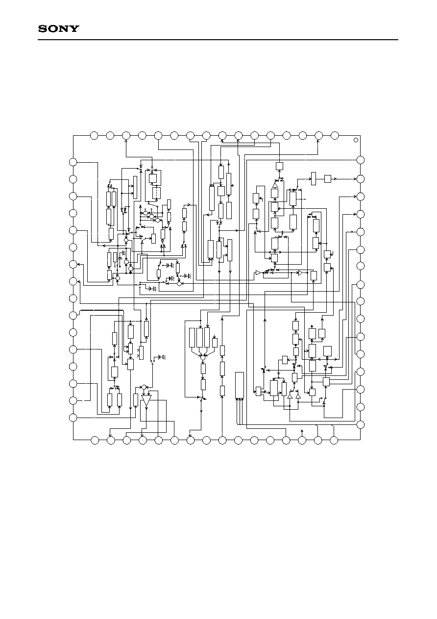
CXA1810AQ/AR
Block Diagram and Pin Configuration
(CXA1810AR)
C
R
O
M
A
E
M
P
H
S
∑
R
E
C
+
A
C
K
∑
R
E
C
B
U
S
D
E
C
O
D
E
R
H
H
K
A
F
C
D
E
T
A
F
C
I
D
A
P
C
I
D
1
/
8
A
P
C
D
E
T
9
0
∞
S
H
I
F
T
A
C
K
B
I
D
D
E
T
A
C
K
C
O
N
T
A
C
K
B
I
D
F
F
f
o
A
U
T
O
C
A
R
C
O
N
V
1
/
N
C
A
R
B
P
F
V
X
O
X
O
V
C
O
B
F
C
X
A
1
8
1
0
A
R
S
W
P
C
A
R
.
C
O
N
T
D
E
V
.
C
O
N
T
S
M
E
A
R
.
C
O
N
T
H
H
S
L
P
F
D
E
M
O
D
L
I
M
L
I
M
M
O
D
S
Y
N
C
S
E
P
C
L
A
M
P
C
L
A
M
P
C
L
A
M
P
C
L
A
M
P
V
I
D
E
O
A
G
C
A
G
C
D
E
T
V
D
/
H
D
I
N
S
E
R
T
Y
M
U
T
E
D
D
S
D
O
C
T
R
A
P
V
C
A
1
C
L
A
M
P
1
S
Y
N
C
A
T
T
A
T
T
B
P
F
A
T
T
L
I
M
T
R
A
P
E
Q
E
Q
f
s
c
T
R
A
P
V
C
A
2
C
L
A
M
P
2
C
L
A
M
P
3
S
h
a
r
p
n
e
s
s
H
P
F
Y
C
O
R
R
E
D
E
T
N
O
I
S
E
C
A
N
C
E
L
L
E
R
W
/
D
C
L
I
P
S
M
E
A
R
C
O
M
P
Y
E
M
P
H
Y
D
E
E
M
P
H
C
L
A
M
P
H
A
R
D
C
L
I
P
H
H
S
C
A
N
C
E
L
S
W
P
C
L
I
P
C
O
M
P
P
I
P
S
R
E
C
C
L
P
F
R
E
C
C
O
N
V
B
U
R
S
T
E
M
P
H
B
U
R
S
T
D
E
E
M
P
H
A
C
C
A
M
P
C
A
R
I
N
V
P
B
C
L
P
F
P
B
C
O
N
V
P
B
C
B
P
F
A
C
C
D
E
T
C
R
O
M
A
D
E
E
M
P
H
S
W
P
A
C
K
S
W
S
W
P
A
C
K
S
W
C
M
U
T
E
I
N
S
E
L
A
G
C
O
F
F
O
N
P
B
S
∑
R
E
C
+
P
B
R
E
C
T
E
S
T
2
R
E
C
T
E
S
T
2
T
E
S
T
1
R
E
C
P
B
C
A
M
R
E
C
T
E
S
T
1
R
E
C
P
B
T
E
S
T
1
R
E
C
P
B
R
E
C
P
B
C
S
E
L
R
E
C
P
B
R
E
C
P
B
P
B
E
D
I
T
P
B
∑
A
C
K
N
O
C
O
R
R
S
∑
R
E
C
W
∑
P
B
P
B
W
∑
P
B
D
O
P
W
∑
P
B
Y
d
P
B
P
B
S
∑
R
E
C
+
A
C
K
∑
R
E
C
Y
d
P
B
P
B
R
E
C
R
E
C
W
∑
P
B
P
B
R
E
C
S
H
P
T
H
R
O
U
E
P
B
+
R
E
C
C
O
R
R
R
E
C
∑
(
S
+
4
4
3
+
E
D
I
T
+
N
O
C
O
R
R
)
A
C
C
C
O
N
T
R
E
C
P
B
S
∑
R
E
C
+
+
+
≠
+
≠
+
+
+
+
+
≠
≠
+
+
+
+
+
+
4
9
5
0
5
1
5
2
5
3
5
4
5
5
5
6
5
7
5
8
5
9
6
0
6
1
6
2
6
3
6
4
1
2
3
4
5
6
7
8
9
1
0
1
1
1
2
1
3
1
4
1
5
1
6
1
7
1
8
1
9
2
0
2
1
2
2
2
3
2
4
2
5
2
6
2
7
2
8
2
9
3
0
3
1
3
2
3
3
3
4
3
5
3
6
3
7
3
8
3
9
4
0
4
1
4
2
4
3
4
4
4
5
4
6
4
7
4
8
Y IN
RE
C L
/
JV
D
V IN
1
AG
C T
C1
V IN
2
WD
C
DD
S/
MA
SK
V
CC
CO
MP
SY
NC
DL
IN
1
AG
C T
C2
DL
O
UT
1
CL
AM
P
TC
2
DL
O
UT
2
CL
AM
P
TC
3
DL
IN
2
C
L
A
M
P
T
C
1
Y
O
U
T
V
O
U
T
G
N
D
V
I
D
E
O
O
U
T
I
N
V
I
N
R
F
/
V
V
C
C
Y
R
F
O
U
T
R
F
G
N
D
Y
R
F
I
N
S
M
E
A
R
C
O
N
T
D
E
V
C
O
N
T
C
A
R
R
C
O
N
T
P
B
C
I
N
S
W
P
C
S
S
I
CK
D.
O.
PU
LS
E
AP
C
FL
AF
C
FL
EX
T
C I
N
DC
F
B
I R
EF
GN
D
X T
AL
IN
V R
EG
X T
AL
OU
T
CA
M F
SC
SH
P
FS
C
OU
T
BF
VC
O
C O
UT
C I
N
C
T
R
A
P
C
T
R
A
P
A
G
C
T
C
3
C
O
M
B
A
D
J
Y
C
O
M
B
O
U
T
L
I
M
C
V
G
1
D
E
E
M
P
H
I
N
C
O
M
P
T
C
R
E
C
C
O
U
T
D
E
M
O
D
O
U
T
N
C
T
C
I
N
E
M
P
H
I
N
S
U
B
E
M
P
H
T
C
M
A
I
N
E
M
P
H
T
C
M
A
I
N
E
M
P
H
O
U
T
C
E
M
P
H
C
O
N
T
--4--
CXA1810AQ/AR
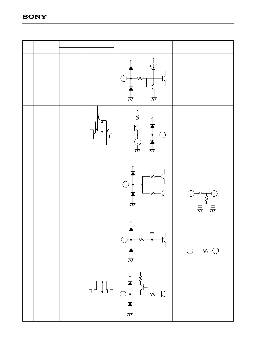
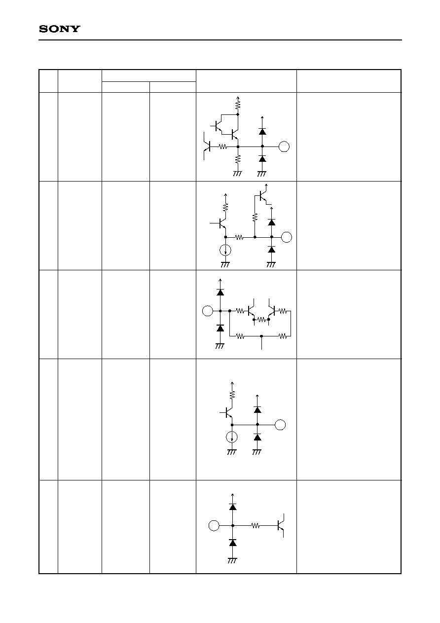
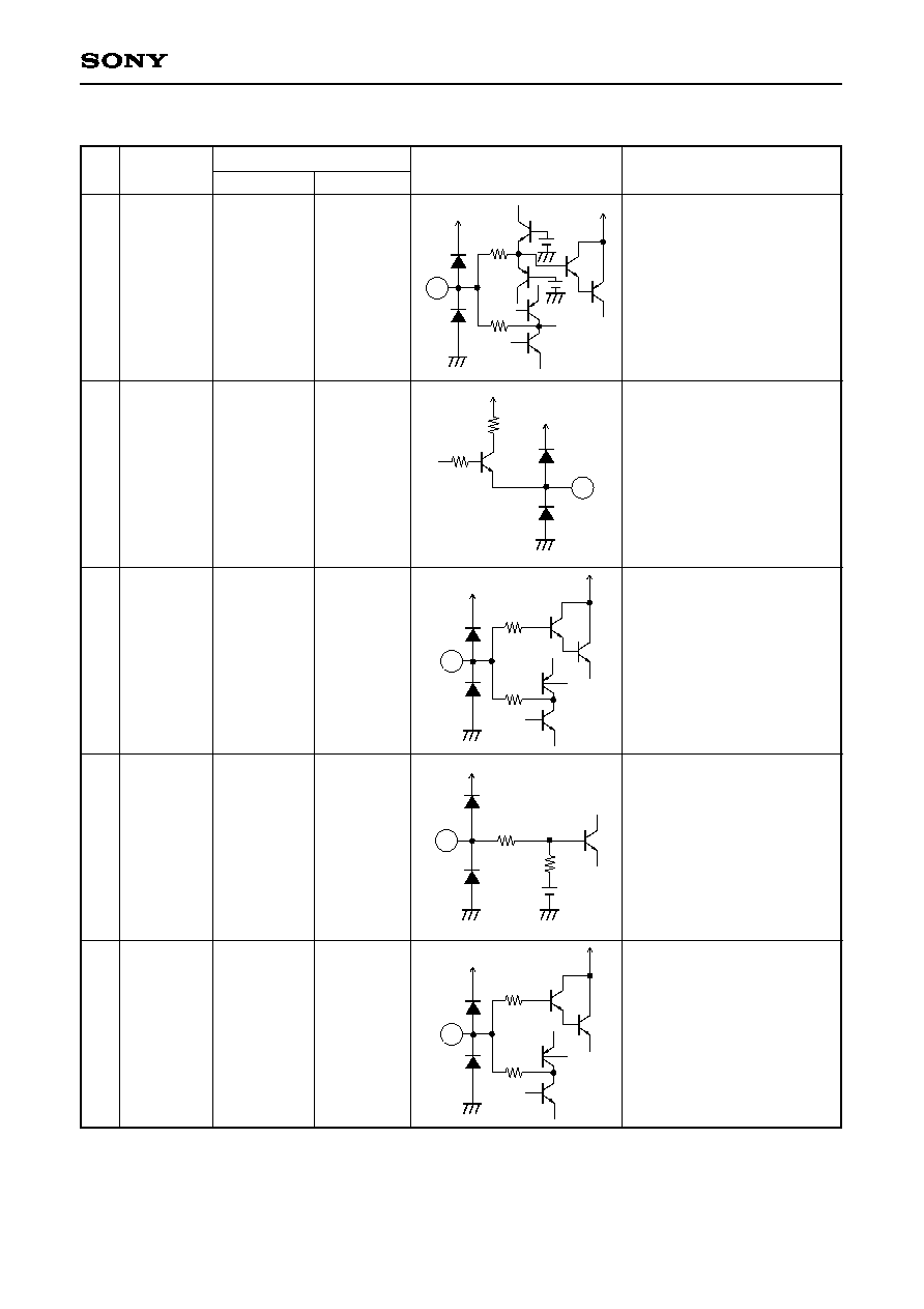
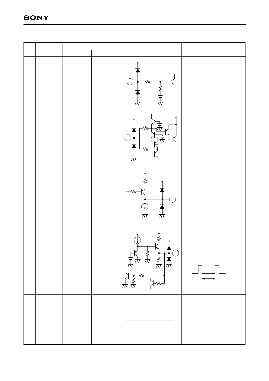
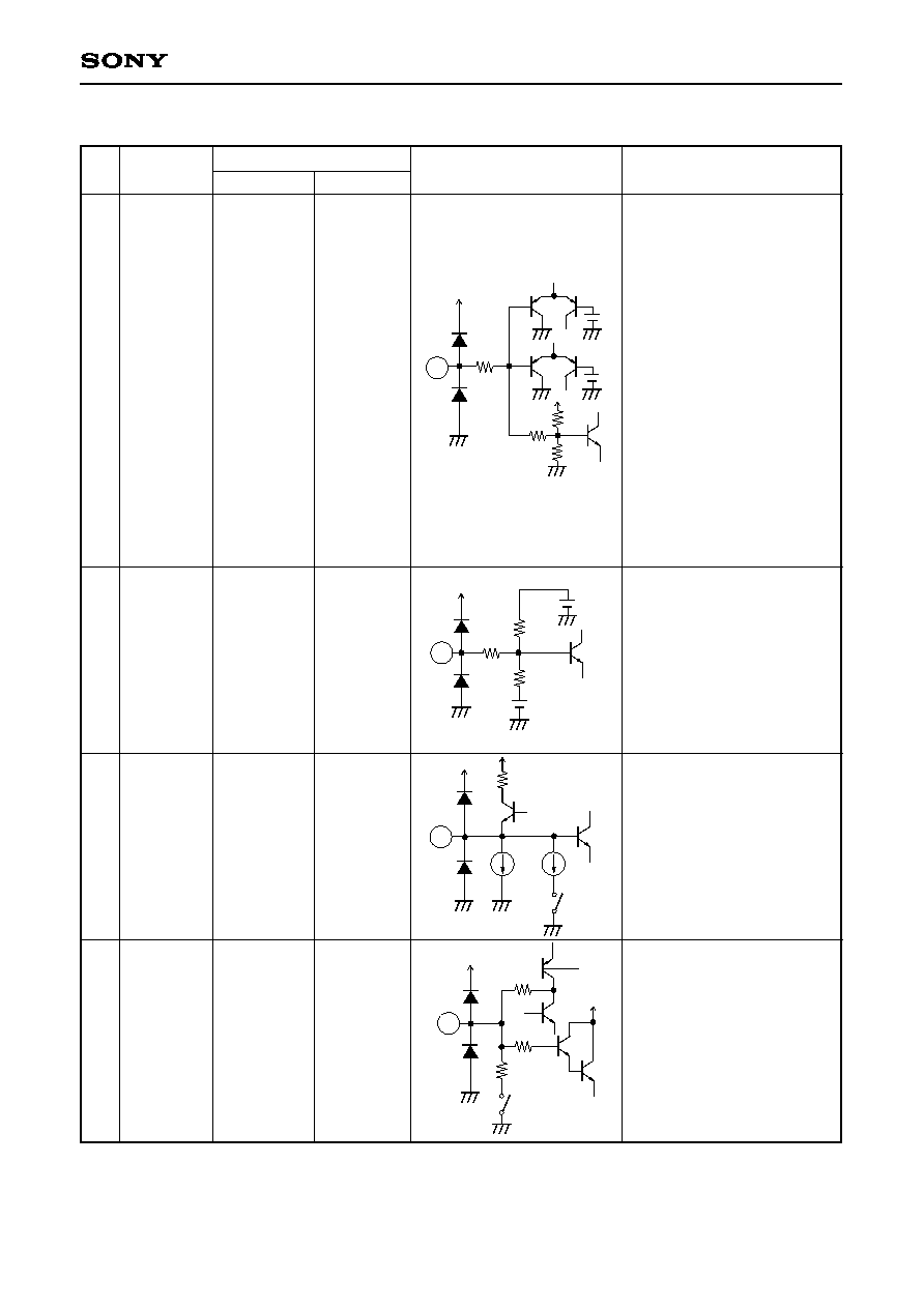
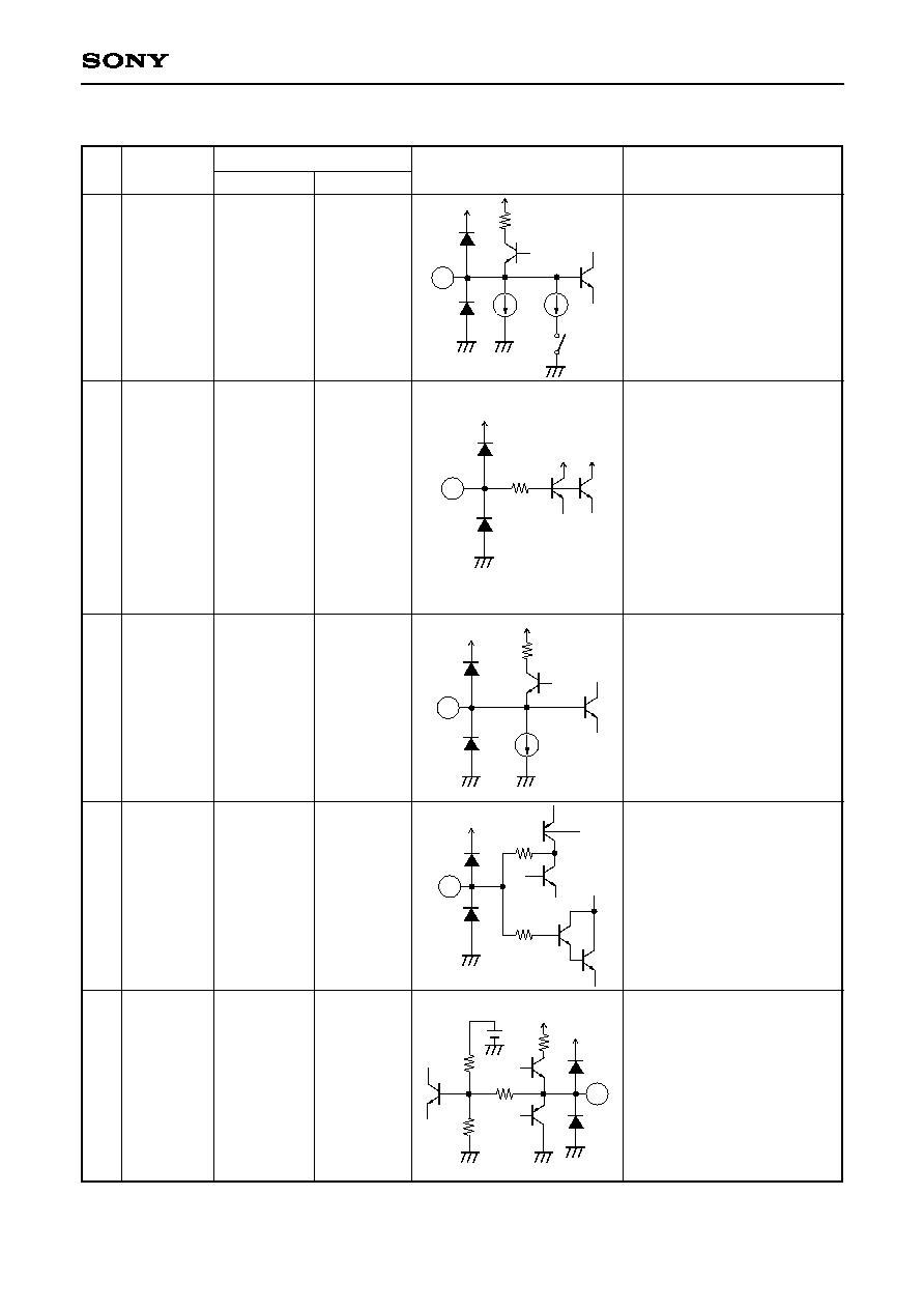
Pin Description
Pin
Symbol
Pin voltage
Equivalent circuit
Description
No.
DC
AC
Chroma emphasis f
0
(center
frequency) adjustment. (Refer
to item 7 on Description of
Operation.)
Main emphasis and main de-
emphasis time constant.
When recording, the
emphasized Y signal prior to
white/dark clipping is output.
Main emphasis and main de-
emphasis time constant.
Apply an external constant
between this pin and Pin 2, as
shown below.
HPF time constant that forms
sub emphasis and sub de-
emphasis. Add resistance
between this pin and Pin 11.
During recording, Y emphasis
input. During playback, this
signal to the noise canceler is
input. Performs diode
clamping (sync tip clamping),
with the clamp capacitance
attached externally.
25µA
150
1
1mA
150
2
4k
100
3
100
4
100
150
5
1
C EMPH
CONT
2
MAIN
EMPH
OUT
3
MAIN
EMPH
TC
4
SUB
EMPH
TC
5
EMPH IN
Control
range:
1.8V to 3.8V
2.05V (sync
tip level)
2.05V (when
time constant
connected)
2.05V (when
time constant
connected)
2.05V (sync
tip level)
--
250mVp-p
output
--
--
500mVp-p
input
2
3
VG1
11
4
--5--
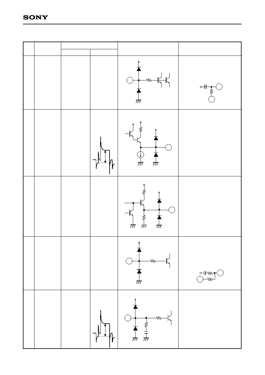
CXA1810AQ/AR
Pin
Symbol
Pin voltage
Equivalent circuit
Description
No.
DC
AC
Connects external time
constant for HPF of noise
canceler. (Refer to item 11 on
Description of Operation.)
Y signal output that has been
FM demodulated and has
passed though the DEMOD
LPF.
During recording, a chroma
signal that has been burst
emphasized, chroma
emphasized, and frequency
converted is output. During
ACK, the output DC goes to
0V. During recording, if
TEST1 is High the burst
emphasized signal is output.
Connects external time
constant for HPF of the
white/dark clipping
compensation circuit during
playback.
Input for de-emphasis circuit
during playback. The signal is
input to the de-emphasis
circuit through the clipping
compensation circuit.
150
6
1mA
63
7
SAT
200
4k
8
150
9
5k
150
2.05V
10
6
NCTC IN
7
DEMOD
OUT
8
REC C
OUT
9
COMP TC
10 DEEMPH
IN
2.05V (when
time constant
connected)
1.6V
2.0V
2.05V (when
time constant
connected)
2.05 V
(center DC)
--
140mVp-p
output during
standard
playback
Low-
frequency
conversion
chroma
signal
300mVp-p
output
--
180mVp-p
input during
playback
VG1
9
11
Input
VG1
6
11
--6--
CXA1810AQ/AR
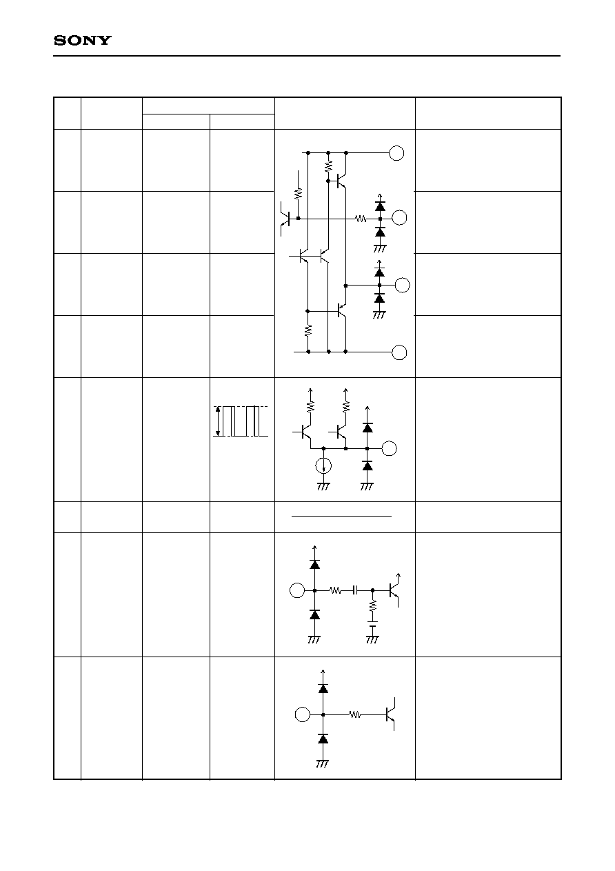
Pin
Symbol
Pin voltage
Equivalent circuit
Description
No.
DC
AC
Internal reference voltage
source. (Can not be used as
external bias for Pins other
than 4, 6, and 9.)
Outputs chroma signal that
has passed through PB C
BPF and chroma feedback
comb filter subtracter
after frequency conversion
during playback.
Connects decoupling
capacitor for limiter of the
playback Y comb block.
Outputs Y signal processed by
comb filter. During playback,
the signal is output through
the sharpness circuit. If mode
E is set High, the signal is
output without passing
through the f sc Trap; if mode
SHP THRU is set High, the
signal is output without
passing through the sharp
-ness circuit.
VCA gain adjustment in the
comb filter block. (Refer to
Adjustment Procedure.)
150
3k
2.5k
11
150
300
0.6mA
270
12
150
150
10k
10k
13
1.4mA
150
14
150
15
11 VG1
12 C TRAP
13 LIM C
14 Y COMB
OUT
15 COMB ADJ
2.05V
2.05V
2.4V
1.2V
(sync tip
level)
Control
range: 1.8V
to Vcc
--
Chroma
signal
300mVp-p
output during
playback
--
Y signal
500mVp-p
output
--
--7--
CXA1810AQ/AR
Pin
Symbol
Pin voltage
Equivalent circuit
Description
No.
DC
AC
Time constant for VCA circuit
in comb filter block. A DC
limiter circuit with an upper
limit of 4.0V and a lower limit
of 2.2V is built in.
Connection for inputting the
playback Y signal to the CCD
DL in a system using two CCD
delay lines. When using this
pin, connect 2.2k
resistance
to GND.
Time constant for feedback
clamp circuit in the comb filter
block.
Inputs CCD DL (delay line)
output signal to the VCA
circuit.
Time constant for feedback
clamp circuit in the comb filter
block.
150
150
16
150
150
17
150
150
18
40k
150
2.1V
19
150
150
20
16 AGC TC3
17 DL IN2
18 CLAMP
TC3
19 DL OUT2
20 CLAMP
TC2
2.2V to 4.0V
2.2V (when
resistance
connected)
--
2.1V (center
DC)
--
--
Video
500mVp-p
output
--
Video
500mVp-p
input
--
--8--
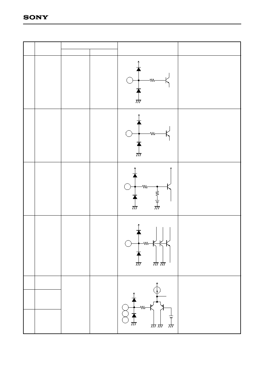
CXA1810AQ/AR
Pin
Symbol
Pin voltage
Equivalent circuit
Description
No.
DC
AC
Inputs CCD DL (delay line)
output signal to VCA circuit.
Time constant for VCA circuit
in the comb filter block. A DC
limiter circuit with an upper
limit of 4.0V and a lower limit
of 2.2V is built in.
Output for inputting a signal to
the CCD DL (delay line).
Normally, Y+C signal is
output. During playback, when
the CCD DL connected to this
pin is used for comb filter
processing of just the C
signal, C signal with quasi
sync is output.
Composite sync signal output.
No output if mode SYNC SEP
OFF is set High.
Main block power supply.
40k
150
2.1V
21
150
150
22
1mA
150
150
23
1H
2.5V
0
270
20k
20k
5k
270
50k
24
21 DL OUT1
22 AGC TC2
23 DL IN1
24 COMP
SYNC
25 V
CC
2.1V (center
DC)
2.2V to 4.0V
2.2V
High :
2.5V,
Low :
0V
output
V
CC
=4.75V
Video
500mVp-p
input
--
Video
500mVp-p
output
--
--
--9--
CXA1810AQ/AR
Pin
Symbol
Pin voltage
Equivalent circuit
Description
No.
DC
AC
Input for VOW (character
level) signal, VOB (character
background) timing pulse of
DDS (date display system)
and masking timing pulse.
MASK :
V
TH
= 1.1V
DDS :
V
TH
= 2.0V
By varying the input DC for
DDS over a range of 2.3V to
3.0V, the character level can
be changed.
(Refer to item 4 on Description
of Operation.)
Determines the white/dark
clipping levels. During open,
the standard white clipping
level is 235%, and the dark
clipping level is 95%.
(Mode DC1, 2 = Low, High)
(Refer to item 5 on Description
of Operation.)
Video signal input. Performs
diode clamping, with the
clamp capacitance externally
connected. If the mode MUTE
is set High, the charge of the
clamp capacitance is
discharged.
Time constant for the video
AGC circuit in the I/O block.
During mute and playback, the
charge of the external
capacitance is discharged.
150
45k
15k
2.0V
1.1V
16k
26
150
2.05V
10k
4.1V
30k
27
270
100nA
4µA
28
MUTE
ON
100
1k
47k
29
MUTE ON
PB ON
26
DDS/MASK
27
WDC
28
V IN2
29
AGC TC1
2.0V
(when open)
(MASK)
1.5V
(DDS)
2.3 to 3.0V
2.6V
(when open)
2.05V
(sync tip
level)
--
--
--
Video
500mVp-p
input
--
--10--
CXA1810AQ/AR
Pin
Symbol
Pin voltage
Equivalent circuit
Description
No.
DC
AC
Video signal input. Performs
diode clamping, with the
clamp capacitance externally
connected. If the mode MUTE
is set High, the charge of the
clamp capacitance is
discharged.
Level adjustment during
recording. The adjustment
range is 1.3V to 2.6V. During
playback, serves as input for
JOG (variable speed
playback) VD pulse and HD
pulse.
V
TH
= 2.7V
(Refer to item 3 on Description
of Operation.)
Video signal input for video
out circuit. Performs diode
clamping, with the clamp
capacitance externally
connected.
Time constant for feedback
clamp circuit in I/O block.
I/O block signal output.
270
100nA
4µA
30
MUTE
ON
150
31
270
100nA
32
100
100
33
3k
150
3.4k
27k
2.05V
34
30 V IN1
31 REC L/JVD
32 Y IN
33 CLAMP TC1
34 Y OUT
2.05V
(sync tip
level)
1.9V
(Typical value
during REC
LEVEL
adjustment)
1.6V
(sync tip
level)
--
1.8V
(sync tip
level)
Video
500mVp-p
input
--
Video
500mVp-p
input
--
Video
500mVp-p
output
--11--
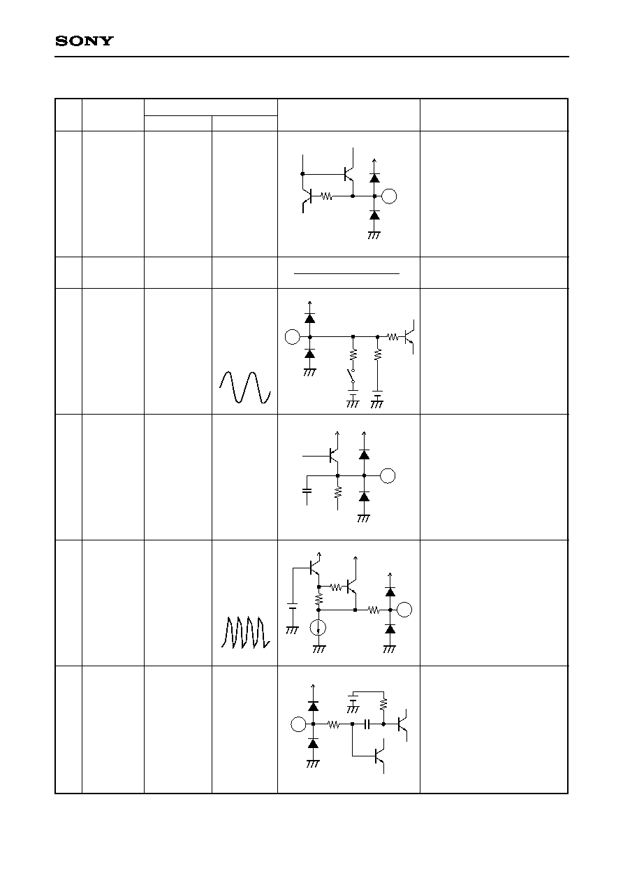
CXA1810AQ/AR
Pin
Symbol
Pin voltage
Equivalent circuit
Description
No.
DC
AC
GND for the video out circuit.
Video out 75
driver output.
Inverted input for V sag
compensation for the video
out 75
driver.
Video out circuit and RF
system block power supply.
During recording, FM-
modulated Y signal output.
If mode TEST2 is set High
during recording, the Y signal
after white/dark clipping is
output.
RF system block GND.
During playback, inputs Y-RF
signal to FM modulation
circuit.
During recording, high
luminance smear
compensation, is performed.
This pin also controls the
signal level for FM modulation
circuit.
100
38
37
36
35
2.5mA
63
63
39
45k
150 10p
41
150
42
35 VOUT GND
36 VIDEO
OUT
37 INV IN
38 RF/V V
CC
39 Y RF OUT
40 RF GND
41 Y RF IN
42 SMEAR
CONT
0V
1.6V
(sync tip
level)
1.5V
V
CC
=4.75V
2.1V
0V
--
Control
range:
1.8V to Vcc
--
Video
2.0Vp-p
output
Video
1.0Vp-p
input
--
Y FM output
500mVp-p
--
YFM
200mVp-p
input
--
--12--
CXA1810AQ/AR
Pin
Symbol
Pin voltage
Equivalent circuit
Description
No.
DC
AC
During recording, adjustment
for deviation of Y-FM
modulation.
During recording, adjustment
for carrier of Y-FM modulation.
During playback, chroma RF
signal input.
PB C LPF is built in, so that a
signal with the AFM and ATF
components (Y RF + C RF)
eliminated can be input.
RF SWP (switching pulse) and
HCHG (head change) pulse
input. Half H shift, HHS
cancel, ACC channel hold,
and PI/PS switching operate
at V
TH
= 0.7V. Yd playback
during playback operates at
V
TH
= 2.05V (same as when
mode Yd is High).
Input to BUS DECODER. CS
is used as chip select, and
data is latched at rising edge.
CK is the clock input. Use a
clock frequency fck of less
than 1.3MHz. SI is used as a
serial input and serial data is
input.
150
43
150
44
50k
150
3.1V
45
150
46
150
2.05V
47
48
49
43 DEV CONT
44 CARR
CONT
45 PB C IN
46 SWP
47 CS
48 SI
49 CK
Control
range:
1.8V to Vcc
Control
range:
1.8V to Vcc
3.1V
(during
playback)
--
High :
Vcc,
Low :
0V
input
--
--
(PB Y RF)
+
(PB C RF
100mVp-p)
input
--
--

--13--
CXA1810AQ/AR
Pin
Symbol
Pin voltage
Equivalent circuit
Description
No.
DC
AC
Drop out pulse input.
V
TH
= 2.05V
If the drop out pulse is input,
the signal prior to 1H is output
for the Y system and the APC
and ACC system errors are
held for the C system.
Connects an APC external
filter.
Connects an AFC external
filter.
During recording, the chroma
signal is input. When the
typical level is 75% color bar
input, the input signal is
314mVp-p.
Connects a DC feedback
external filter for a non-
adjustment VCO.
150
2.05V
100k
50
51
200
PB ON
52
200
200
50k
150
2.6V
53
200
200
200
54
50 D.O.PULSE
51 APC FL
52 AFC FL
53 EXT C IN
54 DCFB
High :
3.1V,
Low :
0V
input
2.25V (typ.)
during lock
2.25V (typ.)
during lock
2.6V
2.25V (typ.)
during lock
--
--
--
(Chroma
signal
314mVp-p
input
--
--14--
CXA1810AQ/AR
Pin
Symbol
Pin voltage
Equivalent circuit
Description
No.
DC
AC
External reference current
source. Connect external
resistance of 18k
to GND.
Be careful concerning pin
cross talk.
Main block GND.
Crystal oscillation reference
input. Be careful concerning
pin cross talk and the floating
capacitance.
4.1V regulator output.
Crystal oscillation reference
output. Connects the crystal
between this pin and Pin 57.
Subcarrier input during
camera recording.
200mVp-p(min). Sharpness
control during playback.
20k
55
4k
2V
270
270
2V
57
PB ON
58
100
15k
310
540µA
59
200
60k
9p
60
55 I REF
56 GND
57 XTAL IN
58 VREG
59 XTAL OUT
60 CAM FSC
SHP
1.8V (when
resistance
connected)
0V
2.0V
4.1V
3.1V
Sharpness
control range:
1.8V to V
CC
--
--
260mVp-p
(NTSC)
during
playback
--
340mVp-p
(NTSC)
during
playback
--
--15--
CXA1810AQ/AR
Pin
Symbol
Pin voltage
Equivalent circuit
Description
No.
DC
AC
Subcarrier output. This
subcarrier is used for the CCD
delay line clock frequency.
Burst flag and VCO OUT
output for testing. When using
this pin, connect 3.3k
resistance to GND. Serves as
VCO output when mode
TEST2 is High.
During recording, outputs
chroma signal after Y/C
separation or for chroma
signal input from Pin 53.
During playback, the playback
chroma signal is output.
During ACK, the output DC
becomes 0V.
Inputs chroma signal to Y/C
MIX circuit in the I/O block.
During component signal
recording or playback, this
signal is Y/C mixed and is
then output from V OUT.
0.5mA
200
61
200
46k
9p
54k
SAT
62
200
2k
100k
63
28k
2.05V
64
61 FSC OUT
62 BF VCO
63 C OUT
64 C IN
2.2V
During BF
output
High :
1.8V,
Low :
0V
Low during
BF interval
2.0V
2.05V
NTSC
600mVp-p
PAL
450mVp-p
550mVp-p
during VCO
output
Chroma
signal
314mVp-p
output
(during
recording)
Chroma
signal
314mVp-p
input

Input conditions
Control DC
Ratings
--16--
CXA1810AQ/AR
No.
1
2
3
4
5
6
7
8
9
10
11
12
13
Measurement item
Composite signal input
Current consumption
during recording
Separate signal input
Current consumption
during recording
Composite signal input
Current consumption in
power saving mode
Separate signal input
Current consumption in
power saving mode
Current consumption
during playback
Internal reference voltage
source 1
Internal reference
voltage source 1
(V
CC
≠)
Internal reference
voltage source 1
(V
CC
+)
Internal reference
voltage source 2
Reference current
source
SYNC AGC
input Low level
SYNC AGC
input High level
PEAK AGC
Symbol
I
REC1
I
REC2
I
PS1
I
PS2
I
PB
V
REG
V
REG≠
V
REG+
V
G1
I
REF
V
AGCL
V
AGCH
V
AGCP
--
--
--
--
--
--
--
--
--
--
e
f
g
--
--
--
--
--
--
--
--
--
--
SG30
Amplitude
--
--
--
--
--
--
--
--
--
--
--
--
--
Frequency
--
--
--
--
--
--
--
--
--
--
--
--
--
--
--
--
--
--
--
--
--
--
--
--
Voltage
--
--
--
--
--
--
--
--
--
--
--
--
--
--
--
--
--
--
--
--
--
SW30
A
C
D
E
F
A
A
A
A
A
B
I
1
I
1
I
1
I
1
I
1
P58
P58
P58
P11
P55
P34
Measurement method
V
CC
=4.75V, voltage at Pin 58 :V
REG
V
CC
=4.5V, voltage at Pin 58 :V
REG1
V
REG
≠=V
REG1
≠V
REG
V
CC
=5.25V, voltage at Pin 58 :V
REG2
V
REG
+=V
REG2
≠V
REG
Voltage at Pin 11
IREF=(voltage at Pin 55 )/18k
Measures the output SYNC level.
Measures the output amplitude level.
Min.
63
55
20
35
68
3.90
≠12
1.95
94
Typ.
88
78
30
53
94
4.13
≠1
+1
2.08
100
143
143
550
Max.
113
100
40
70
120
4.36
+12
2.21
106
Unit
mA
mA
mA
mA
mA
V
mV
mV
V
µ
A
mV
mV
mV
Electrical Characteristics
V
CC
= 4.75V, Ta = 25
∞
C, see Electrical Characteristics Measurement Circuit and BUS DECODER Mode Condition Table.
Start measurements after adjustments in accordance with the Precautions Concerning Measurements.
)
Video AGC
Signal
Signal
source
Voltage
source
SW
Mode
Measu-
set to
condi-
rement
ON
tions
point
<Current consumption, reference bias source>
<Y recording>
(

--17--
CXA1810AQ/AR
Input conditions
Control DC
Ratings
No.
14
15
16
17
18
19
20
21
22
23
24
25
Measurement item
For video AGC off
For video AGC on
300kHz gain for
TRAP off
300kHz gain for
TRAP on
fsc TRAP
3.58MHz gain
Hard clip amount
White clip amount
Dark clip amount
≠3dB
500kHz
≠3dB
2MHz
≠10dB
2MHz
≠20dB
2MHz
Symbol
F
IO1
F
IO2
G
YC1
G
YC2
G
YC3
K
H.C
K
W.C
K
D.C
F
E11
F
E12
F
E13
F
E14
d
d
b
c
b
a
SG30
SG30
SG5-1
SG5-1
SG5-2
Amplitude
Sine wave
357mVp-p
Sine wave
357mVp-p
500mVp-p
647mVp-p
500mVp-p
≠3dB
(354mVp-p)
≠10dB
(158mVp-p)
≠20dB
(50mVp-p)
Frequency
300kHz
/5MHz
300kHz
300kHz
3.58MHz
--
--
10kHz/
500kHz
10kHz/
2MHz
--
--
--
--
--
Voltage
--
--
--
--
--
SW30
SW30
SW5-1
SW5-1
SW5-1
SW5-3
A
B
G
C
H
H
H
P34
P14
P39
P39
P39
Measurement method
Level ratio between 300kHz sine wave and
5MHz sine wave
I/O gain of 300kHz sine wave
(Refer to output waveform measurement
Nos. 14 and 15.)
Level ratio between 300kHz sine wave and
3.58MHz sine wave (Refer to output
waveform measurement Nos. 14 and 15.)
Level ratio of this signal output with
500mVp-p input and with
647mVp-p input
Measures the level ratio of
each output frequency
component.
(These emphasis
characteristics include white/
dark clipping.)
Min.
≠1.5
≠1.5
10.7
11.8
15.0
19.5
Typ.
0
0
≠0.3
≠0.6
≠23
115
235
95
Max.
1.5
1.5
≠14
11.7
15.8
19.0
25.5
Unit
dB
dB
dB
dB
dB
%
%
%
dB
dB
dB
dB
Pre-emphasis standard
frequency characteristics
I/O frequency
characteristics
Y COMB OUT frequency
characteristics
X
Y
Z
Y
X
Z
X
K
W
.
C
=
--
◊
1
0
0
K
D
.
C
=
--
◊
1
0
0
Signal
Signal
source
Voltage
source
SW
Mode
Measu-
set to
condi-
rement
ON
tions
point
V (500kHz)
V (10kHz)
V (2MHz)
V (10kHz)
--18--
CXA1810AQ/AR
Input conditions
Control DC
Ratings
No.
26
27
28
29
30
31
32
33
34
35
36
37
38
39
Measurement item
≠3dB
200kHz
≠3dB
2MHz
≠10dB
2MHz
≠20dB
2MHz
Output level
Secondary distortion
Carrier control
minimum frequency (L)
Carrier control
maximum frequency (L)
Carrier control
minimum frequency (E)
Carrier control
maximum frequency (E)
Deviation control
minimum frequency (L)
Deviation control
maximum frequency (L)
Deviation control
minimum frequency (E)
Deviation control
maximum frequency (E)
Symbol
F
E21
F
E22
F
E23
F
E24
V
MOD
D
MOD
CL MIN
CL MAX
CE MIN
CE MAX
DL MIN
DL MAX
DE MIN
DE MAX
a
--
SG5-2
--
Amplitude
≠3dB
(354mVp-p)
≠10dB
(158mVp-p)
≠20dB
(50mVp-p)
--
Frequency
10kHz/
200kHz
10kHz/
2MHz
--
--
--
V44
V44
V44
V44
V5-1
V43
V5-1
V43
V5-1
V44
V43
V5-1
V44
V43
Voltage
--
--
1.8V
4.75V
1.8V
4.75V
V
G1
+0.5V
1.8V
V
G1
+0.5V
4.75V
V
G1
+0.5V
Adjusted value
1.8V
V
G1
+0.5V
Adjusted value
4.75V
SW5-1
SW5-3
SW3-2
--
SW5-2
A
A
I
A
I
P2
P39
Measurement method
Measures the level ratio
V (200kHz)
of each output frequency
V (10kHz)
component.
V (2MHz)
(These emphasis
V (10kHz)
characteristics do not
include white/dark
clipping.)
Signal level with
4.2MHz output
Ratio to secondary higher harmonic
components with 4.2M output
V (8.4MHz)/V (4.2MHz)
Measures the
output frequency.
Makes initial setting of V44, applies test 9
measurement V
G1
+0.5V to V5-1 and then
measures the output frequency.
After setting V44 to mode condition I and
adjusting the initial setting of the SW
conditions so that the output frequency is
5.7MHz, applies test 9 measurement
V
G1
+0.5V to V5-1 and then measures the
output frequency.
Min.
2.7
14.5
17.1
19.5
440
4.2
5.7
5.4
7.7
Typ.
500
≠34
3
5.2
4.7
6.8
5.0
5.9
7.0
8.0
Max.
3.3
16.5
19.1
23.5
560
4.2
5.7
5.4
7.7
Unit
dB
dB
dB
dB
mVp-p
dB
MHz
MHz
MHz
MHz
MHz
MHz
MHz
MHz
Hi-8 pre-emphasis
Signal
Signal
source
Voltage
source
SW
Mode
Measu-
set to
condi-
rement
ON
tions
point
FM modulator
--19--
CXA1810AQ/AR
Input conditions
Control DC
Ratings
No.
40
41
42
43
44
45
46
47
48
49
Measurement item
Linearity (L)
Linearity (E)
PB Y comb filter ATT level
HHS canceler
EDIT
MIN
MAX
Symbol
L
MODL
L
MODE
K
0
K
1
K
2
K
3
V
DEHHS
F
SHP0
F
SHP1
F
SHP2
--
a
--
a
--
SG3
--
SG3
Amplitude
--
30mVp-p
--
175mVp-p
Frequency
--
300kHz
--
300kHz/
2.15MHz
V5-1
V5-1
V44
--
--
--
V60
V60
Voltage
V
G1
V
G1
+0.25V
V
G1
+0.5V
V
G1
V
G1
+0.25V
V
G1
+0.5V
Adjusted
value
--
--
--
1.8V
4.75V
SW5-2
SW3-1
SW4
FW17
SW46-1
ON/OFF
SW3-1
SW4
A
I
J
1
J
2
J
3
J
4
F
K
F
P39
P14
P17
P14
Measurement method
Makes initial setting of V44, applies test 9
measurement V
G1
, V
G1
+0.25V and
V
G1
+0.5V to V5-1 and then calculates the
following equation using the output
frequency.
(V
G1
+0.5V)≠(V
G1
+0.25V)
(V
G1
+0.25V)≠(V
G1
)
After setting V44 to mode condition I and
adjusting the initial setting of the SW
conditions so that the output frequency is
5.7MHz, applies test 9 measurement, V
G1
,
V
G1
+0.25V, and V
G1
+0.5V to V5-1 and
then calculates the following equation using
the output frequency:
(V
G1
+0.5V)≠(V
G1
+0.25V)
(V
G1
+0.25V)≠(V
G1
)
Measures the I/O gain under all mode
conditions.
DC level difference at P17 (Pin 17
DL IN2) when SW46-1 is turned on and off
Measures the level ratio of P14 (Pin 14 Y
COMB OUT) output between 300kHz input
and 2.15MHz input.
V (2.15MHz)
V (300kHz)
Min.
0.9
0.9
≠7.8
≠9.3
≠21
Typ.
1.0
1.0
≠4.8
≠6.3
≠18
≠32
1.6
≠1.0
≠10
7
Max.
1.1
1.1
≠1.8
≠3.3
≠15
Unit
--
--
dB
dB
dB
dB
mV
dB
dB
dB
FM modulator
Signal
Signal
source
Voltage
source
SW
Mode
Measu-
set to
condi-
rement
ON
tions
point
PB sharpness frequency
characteristics
<Y playback>
--20--
CXA1810AQ/AR
Input conditions
Control DC
Ratings
No.
50
51
52
53
54
55
56
57
58
59
60
61
62
Measurement item
NC1
≠3dB
1MHz
≠20dB
1MHz
≠30dB
1MHz
NC2
≠30dB
1MHz
NC3
≠30dB
1MHz
NC4
≠30dB
1MHz
NC5
≠30dB
1MHz
Gain (L)
Linearity (L)
Gain (E)
Linearity (E)
Carrier leak
DOC Trap
Symbol
F
NC10
F
NC11
F
NC12
F
NC2
F
NC3
F
NC4
F
NC5
G
DEMOD1
L
DEMOD1
G
DEMOD2
L
DEMOD2
CL
DEMOD
G
TRAP
a
a
a
SG5-2
SG41
SG19
Amplitude
≠3dB
(354mVp-p)
≠20dB
(50mVp-p)
≠30dB
(15.8mVp-p)
200mVp-p
300mVp-p
Frequency
10kHz/
1MHz
3MHz
5MHz
7MHz
4MHz
7MHz
10MHz
4.2M
300kHz/
3.58MHz
--
--
--
Voltage
--
--
--
SW5-1
SW5-3
SW6
SW24-1
SW33
SW41
SW17
SW19
SW20
SW22
SW50
L1
L2
L3
L4
L5
F
M
F
T
P34
P7
P17
P23
Measurement method
Measures the level ratio of each
output frequency component.
V (1MHz)
V (10kHz)
Calculates the
V (7M)≠V (3M)
equations at right
7-3
with the output DC
V (7M)≠V (5M)
at P7 (Pin 7
V (5M)≠V (3M)
DEMOD OUT) for
V (10M)≠V (4M)
each input
10≠4
frequency.
V (10M)≠V (7M)
V (7M)≠V (4M)
Ratio of 4.2M
component of output to
input
Level ratio of P17 (Pin 17 DL IN2) and
P23 (Pin 23 DL IN1) between 300kHz
input and 3.58MHz input
V (3.58MHz)
V (300kHz)
Min.
90
0.9
50
0.9
Typ.
0
≠2.9
≠6.3
≠6.7
≠5.0
≠2.5
≠4.6
115
0.96
65
1.02
≠40
≠28
Max.
140
1.1
80
1.1
≠14
Unit
dB
dB
dB
dB
dB
dB
dB
mV
MHz
--
mV
MHz
--
dB
dB
Noise canceler frequency characteristics
FM demodulation
Signal
Signal
source
Voltage
source
SW
Mode
Measu-
set to
condi-
rement
ON
tions
point
--21--
CXA1810AQ/AR
Input conditions
Control DC
Ratings
No.
63
64
65
66
67
68
69
70
71
72
73
74
75
76
77
Measurement item
300kHz gain
2.5MHz frequency
characteristic
6.12MHz frequency
characteristic
300kHz gain
4.0MHz frequency
characteristic
7.8MHz frequency
characteristic
VOB
VOW
JOG VD
High
level
Low
level
Pulse width
Delay
Amplifier gain
5MHz frequency
characteristic
Symbol
G
LPF11
F
LPF12
F
LPF13
G
LPF21
F
LPF22
F
LPF23
V
VOB
V
VOW
J
OGVD
V
CS-H
V
CS-L
W
CS
D
CS
G
BUFF
F
BUFF
h
d
SG41
SG26
SG30
SG30
SG31
SG30
SG32
Amplitude
200mVp-p
--
--
Sine wave
357mVp-p
Frequency
300kHz
2.5MHz
6.12MHz
300kHz
4.0MHz
7.8MHz
--
--
300kHz
300kHz
/5MHz
--
--
--
--
Voltage
--
--
--
--
SW41
SW26
SW30
SW30
SW31
SW30
SW32
F
M
B
B
A
P7
P34
P24
P24
P34
P36
Measurement method
(300kHz I/O gain) ≠
(compensation item G
C1
)
V (2.5MHz)
V (300kHz)
V (6.12MHz)
V (300kHz)
(300kHz I/O gain) ≠
(compensation item G
C2
)
V (4.0MHz)
V (300kHz)
V (7.8MHz)
V (300kHz)
Refer to Detailed
Explanation of
Measurement
Method (2).
P24 ( 24 COMP SYNC)
P34 ( 34 YOUT)
Measures the I/O gain for a 300kHz sine wave
overlapping the Y signal.
Measures the level ratio for a 300kHz sine wave
and 5MHz sine wave overlapping the Y signal.
Min.
≠1.5
≠1.5
≠1.5
≠0.5
≠10
≠15
2.3
0.1
5.5
Typ.
0
0
≠38
0
1.0
≠16
15
340
10
2.5
0.03
4.5
0.35
6.0
0
Max.
1.5
1.5
≠32
1.5
2.0
≠10
40
35
2.7
0.2
0.7
6.5
Unit
dB
dB
dB
dB
dB
dB
mV
mV
mV
V
V
µ
sec
µ
sec
dB
dB
Demodulation LPF frequency characteristics
Standard mode
Refer to Detailed Explanation (1).
Refer to Detailed Explanation (2).
Hi-8 mode
DDS
(Date display system)
Composite sync pulse
Video buffer
Calculates the
equations at left using
the output level of P7
(Pin 7 DEMOD OUT)
for each input
frequency.
Refer to Detailed
Explanation of
Measurement Method
(1) for compensation
values G
C1
and G
C2
.
The amplitude
frequency indicated for
the input conditions is
the value of SG54 in
SG41.
Measures the DC
level difference with
the pedestal level.
Measures the DC
level difference with
the sync tip level.
W
C
S
D
C
S
G
N
D
V
C
S
-
L
V
C
S
-
H
<Y recording/playback>
Signal
Signal
source
Voltage
source
SW
Mode
Measu-
set to
condi-
rement
ON
tions
point

--22--
CXA1810AQ/AR
Input conditions
Control DC
Ratings
No.
78
79
80
81
82
83
84
85
86
87
88
89
90
91
Measurement item
C OUT LEVEL 1
(REC)
C OUT LEVEL 2
(S∑REC)
Gain
Maximum
gain
Minimum
gain
Burst emphasis
level
0dB
sc
0dB
+500kHz
0dB
≠500kHz
≠10dB
sc
≠10dB
+500kHz
≠10dB
≠500kHz
ACK OFF
ACK ON
Symbol
G
COUT1
G
COUT2
G
CENACC
G
MAXACC
G
MINACC
BE
V
CE1
F
CE11
F
CE12
V
CE2
F
CE21
F
CE22
V
ACK OFF
V
ACK ON
d
a
a
a
i
a
SG30
SG53
SG53
SG53
SG53
SG53
Amplitude
Sine wave
314mVp-p
314mVp-p
143mVp-p
10mVp-p
363mVp-p
143mVp-p
VC=
314mVp-p
VC=
99.3mVp-p
20mVp-p
2mVp-p
Frequency
3.58MHz
3.58MHz
3.58MHz
3.58MHz
3.58MHz
4.08MHz
3.08MHz
3.58MHz
4.08MHz
3.08MHz
3.58MHz
--
--
--
--
--
--
Voltage
--
--
--
--
--
--
SW30
SW53
SW24-1
SW24-2
SW53
SW24-1
SW24-2
SW53
SW24-1
SW24-2
SW53
SW24-1
SW24-2
SW53
N
O
P
P
P
Q
P63
P8
P8
P8
P63
Measurement method
Measures the I/O level ratio for 3.58MHz
sine wave.
Measures the I/O level ratio.
Until measurement No. 126, input signal
1 from SG24.
Measures the level ratio between the output
burst interval and the chroma interval.
V
OB
V
OC
Measures the output level for the input
frequency of the chroma interval. V
CE1
Measures the ratio between V
CE1
and the
output level for the input frequency of the
chroma interval.
Measures the output level for the input
frequency of the chroma interval. V
CE2
Measures the ratio between V
CE2
and the
output level for the input frequency of the
chroma interval.
Measures the output DC level.
Min.
≠1.5
≠1.5
≠3.3
14
5.0
200
≠1.4
≠1.4
60
1.4
1.4
1.7
Typ.
0
≠0.3
≠1.3
18
≠9.5
6.0
270
1.0
1.0
85
3.0
3.0
2.0
80
Max.
1.5
1.5
0.7
≠7
7.0
360
2.6
2.6
120
5.4
5.4
2.3
200
Unit
dB
dB
dB
dB
dB
dB
mVp-p
dB
dB
mVp-p
dB
dB
V
mV
ACC AMP
C OUT DC
V
O
B
V
O
C
Signal
Signal
source
Voltage
source
SW
Mode
Measu-
set to
condi-
rement
ON
tions
point
Chroma emphasis characteristics
<C recording>
--23--
CXA1810AQ/AR
Input conditions
Control DC
Ratings
No.
92
93
94
95
96
97
98
99
100
101
102
103
104
Measurement item
REC C RF
LEVEL
REC chroma band 1
(≠750kHz)
REC chroma band 2
(≠300kHz)
REC chroma band 3
(+300kHz)
REC chroma band 4
(+650kHz)
Upper
pull-in range
Lower
pull-in range
Upper
pull-in range
Lower
pull-in range
Upper
pull-in range
Lower
pull-in range
Upper
pull-in range
Lower
pull-in range
Symbol
V
RECC
F
RECC1
F
RECC2
F
RECC3
F
RECC4
APCRN+
APCRN≠
APCRP+
APCRP≠
AFCN+
AFCN≠
AFCP+
AFCP≠
i
a
j
I
SG53
SG53
SG24
Amplitude
VC=
314mVp-p
143mVp-p
--
Frequency
3.58MHz
2.83MHz
3.28MHz
3.88MHz
4.23MHz
3.58MHz
+
Hz
3.58MHz
≠
Hz
4.43MHz
+
Hz
4.43MHz
≠
Hz
16.206kHz
(+3%)
15.262kHz
(≠
3%)
16.094kHz
(+3%)
15.156kHz
(≠
3%)
--
--
--
Voltage
--
--
--
SW24-1
SW24-2
SW53
SW24-1
SW24-2
SW53
SW24-1
SW24-2
SW51
SW53
SW57
SW59
SW24-1
SW24-2
SW62
Q
Q
R
S
1
S
2
S
3
S
4
P8
P61
P62
Measurement method
Measures the output level of the
chroma interval. V
RECC
Measures the ratio between V
RECC
and the output level of the chroma
interval.
The output frequencies of 3.58MHz +
kHz are converted to
743kHz≠
kHz for frequency
conversion.
Upper input frequency pulled in within
2 seconds by the SG53 input
frequency (3.58MHz+1kHz).
Lower input frequency pulled in within
2 seconds by the SG53 input
frequency (3.58MHz≠3kHz).
Upper input frequency pulled in within
2 seconds by the SG53 input
frequency (4.43MHz +
1kHz).
Lower input frequency pulled in within
2 seconds by the SG53 input
frequency (4.43MHz≠3kHz).
Measures the output frequency 1
second later after switching the mode
conditions.
Min.
210
230
200
Typ.
300
≠40
≠2.0
2.5
≠1.0
6125979
5769126
6035156
5683594
Max.
420
≠230
≠200
Unit
mVp-p
dB
dB
dB
dB
Hz
Hz
Hz
Hz
Hz
Hz
Hz
Hz
REC APC pull-in
range (NTSC)
REC APC pull-in
range (PAL)
REC AFC pull-in
range (NTSC)
REC AFC pull-in
range (PAL)
REC C RF level
Signal
Signal
source
Voltage
source
SW
Mode
Measu-
set to
condi-
rement
ON
tions
point
--24--
CXA1810AQ/AR
Input conditions
Control DC
Ratings
No.
105
106
107
108
109
110
111
112
113
114
115
116
117
Measurement item
PB C OUT
level
PB chroma band 1
(≠650kHz)
PB chroma band 2
(≠300kHz)
PB chroma band 3
(+300kHz)
PB chroma band 4
(+1.2MHz)
Gain difference
between channels 1-2
Gain difference
between channels 1-3
Gain difference
between channels 1-4
High-speed ACC
compression ratio
Burst de-emphasis level
Frequency deviation
Output level
Secondary distortion
Symbol
V
PBCO
F
PBC1
F
PBC2
F
PBC3
F
PBC4
G
CH12
G
CH13
G
CH14
F
ACC
B
DE
XON
V
XON
HD
2XON
n
a/k
o
m
a
--
SG45
SG45
SG46
SG53
SG45
--
Amplitude
VC=
200mVp-p
200mVp-p
1.4Vo-p
--
200mVp-p
--
Frequency
743kHz
100kHz
443kHz
1043kHz
1.9MHz
743kHz
50Hz
--
743kHz
--
--
--
--
--
--
Voltage
--
--
--
--
--
SW16
SW18
SW24-1
SW24-2
SW45
SW16
SW18
SW24-1
SW24-2
SW45
SW46-1
SW46-2
SW24-1
SW24-2
SW53
SW16
SW18
SW24-1
SW24-2
SW45
T
T
U
T
F
P63
P63
P8
P63
P61
Measurement method
Measures the output level of the
chroma interval. V
PBCO
Measures the ratio between V
PBCO
and the output level of the chroma
interval.
The output frequencies of 743kHz
+
kHz are converted to
3.58MHz≠
kHz for frequency
conversion.
Refer to Detailed Explanation of
Measurement Method (3). Measures
the gain difference between channels.
Refer to Detailed Explanation of
Measurement Method (4).
Measures the level ratio between the
burst interval and the chroma interval
of output.
V
OB
V
OC
Difference between output frequency
and
SCN
=3579545Hz.
XON
=
XON
≠
SCN
Measures the output level.
Ratio with secondary higher harmonic
component.
V (7.16MHz)/V (3.58MHz)
Min.
130
≠0.5
≠0.5
≠0.5
≠5.5
≠50
450
Typ.
200
≠2.4
≠0.5
≠2.3
≠40
0
0
0
0.6
≠4.5
600
≠45
Max.
300
0.5
0.5
0.5
3.0
≠3.5
50
750
≠25
Unit
mVp-p
dB
dB
dB
dB
dB
dB
dB
dB
dB
Hz
mVp-p
dB
PB C OUT level
PB ACC gain differencebetween channels
XO characteristics (NTSC)
V
O
C
V
O
B
<C playback>
Signal
Signal
source
Voltage
source
SW
Mode
Measu-
set to
condi-
rement
ON
tions
point
--25--
CXA1810AQ/AR
Input conditions
Control DC
Ratings
No.
118
119
120
121
122
123
124
125
126
Measurement item
Frequency deviation
Output level
Secondary distortion
Upper
pull-in range
Lower
pull-in range
Upper
pull-in range
Lower
pull-in range
Delay
Pulse width
Symbol
XOP
V
XOP
HD
2
XOP
APCN+
APCN≠
APCP+
APCP≠
T
d
BF
W
d
BF
--
a
l
a
l
a
l
a
l
b
--
SG45
SG24
SG45
SG24
SG45
SG24
SG45
SG24
SG5-1
Amplitude
--
200mVp-p
--
200mVp-p
--
200mVp-p
--
200mVp-p
--
--
--
--
--
--
--
--
Voltage
--
--
--
--
--
--
SW57
SW59
SW16
SW18
SW24-1
SW24-2
SW45
SW62
SW16
SW18
SW24-1
SW24-2
SW45
SW51
SW57
SW59
SW62
SW5-1
SW24-1
SW24-2
SW62
F
V
1
V
2
V
3
V
4
F
P61
P62
P62
Measurement method
Difference between output frequency
and
SCP
= 4433619Hz.
f
XOP
=
XOP
≠
SCP
Measures the output level.
Ratio with secondary higher harmonic component
V (8.86MHz)/V (4.43MHz)
Measures the output frequency 1
second later after switching the mode
conditions.
Min.
≠50
320
3.5
3.3
Typ.
460
≠40
6125979
5769126
6035156
5683594
4.1
4.3
Max
50
650
≠25
4.7
5.3
Unit
Hz
mVp-p
dB
Hz
Hz
Hz
Hz
µ
sec
µ
sec
XO characteristics (PAL)
PB APC
pull-in range (PAL)
Burst flag
PB APC
pull-in range (NTSC)
T
d
B
F
W
d
B
F
P
2
4
(
2
4
C
O
M
P
S
Y
N
C
)
P
6
2
(
6
2
B
F
O
U
T
)
Signal
Signal
source
Voltage
source
SW
Mode
Measu-
set to
condi-
rement
ON
tions
point
Frequency
--
765.747kHz
(+3%)
16.206kHz
(+3%)
721.141kHz
(≠
3%)
15.262kHz
(≠
3%)
754.395kHz
(+3%)
16.094kHz
(+3%)
710.449kHz
(≠
3%)
15.156kHz
(≠
3%)
--
--26--
CXA1810AQ/AR
Electrical Characteristics Measurement Circuit
R
1
7
5
6
0
0
V
2
0
2
.
7
v
C
1
8
1
0
µ
V
2
2
2
.
8
v
L
1
2
2
µ
H
R
5
3
3
0
0
(
1
%
)
A
I
1
V
C
C
S
G
3
2
S
G
3
1
S
G
3
0
S
W
3
2
S
W
3
1
S
W
3
0
C
2
6
0
.
4
7
µ
V
3
1
C
2
5
1
0
µ
C
2
4
0
.
4
7
µ
R
1
0
4
7
k
C
2
3
1
0
µ
C
2
2
0
.
4
7
µ
C
2
1
0
.
0
1
µ
S
G
2
6
S
W
2
6
C
2
0
1
0
µ
S
G
2
4
C
1
9
1
0
0
µ
SW
24-
2
SW
24-
1
P
2
4
P
2
3
C
1
7
1
0
µ
C
1
6
3
.
3
µ
C
1
4
3
.
3
µ
C
1
5
1
0
µ
SW
22
SW
20
S
G
1
9
V
1
8
2
.
7
v
SW
19
S
W
1
6
V
1
6
2
.
8
v
V
1
5
3
v
C
1
3
1
0
µ
P
1
1
P
8
P
7
C
1
2
1
0
µ
C
1
1
0
.
0
1
µ
C
1
0
1
0
µ
C
9
4
7
µ
C
8
4
7
0
p
R
8
1
k
R
7
1
k
R
6
1
k
S
W
6
S
G
5
-
2
V
5
-
2
2
.
3
7
v
S
G
5
-
1
S
W
5
-
3
C
6
0
.
4
7
µ
C
7
2
2
0
p
S
W
5
-
1
S
W
5
-
2
V
5
-
1
S
W
4
R
4
1
2
0
0
S
G
3
S
W
3
-
1
S
W
2
C
5
0
.
4
7
µ
R
2
3
9
0
(
1
%
)
S
W
3
-
2
R
1
4
7
0
(
1
%
)
C
4
1
5
0
p
C
3
1
5
0
p
C
2
3
3
0
p
C
1
3
9
0
p
V
1
P
2
C
4
5
1
0
µ
C
4
4
0
.
0
1
µ
C
4
3
1
0
0
0
p
P
5
8
P
6
3
P
6
2
P
6
1
P
5
5
SW
59
SW
62
SW
57
(
P
A
L
)
(
N
T
S
C
)
R
1
9
3
.
3
k
V
6
0
3
v
C
4
1
8
2
p
C
4
2
0
.
0
1
µ
R
1
8
1
8
k
C
4
0
1
µ
R
1
6
3
9
0
0
R
1
5
6
8
0
0
C
3
8
0
.
6
8
µ
0.0
22µ
C
3
6
1
µ
S
G
5
3
S
W
5
3
C39
1
000
p
S
W
5
1
S
W
5
0
V
5
0
3
v
C
3
3
1
µ
C
3
5
6
8
0
0
p
C
3
4
3
3
0
p
µ
-
C
O
M
S
G
4
6
S
W
4
6
-
2
S
W
4
6
-
1
V
4
6
1
.
4
v
S
W
4
5
S
G
4
5
S
G
4
1
V
4
4
C
3
2
1
0
0
p
V
4
3
3
v
V
4
2
3
v
S
W
4
1
C
3
1
0
.
0
1
µ
C
3
0
1
0
µ
P
3
9
P
3
6
P
3
4
R
1
4
1
k
R
1
2
7
5
R
1
1
1
k
C
2
8
2
2
0
C
2
9
2
.
2
µ
S
W
3
3
C
2
7
1
µ
V
3
3
1
v
R
3
1
2
0
0
(
1
%
)
C
X
A
1
8
1
0
A
R
C37
1
6
1
5
1
4
1
3
1
2
1
1
1
0
9
8
7
6
5
4
3
2
1
6
4
6
3
6
2
6
1
6
0
5
9
5
8
5
7
5
6
5
5
5
4
5
3
5
2
5
1
5
0
4
9
4
2
4
3
4
4
4
5
4
6
4
7
4
8
3
5
3
6
3
7
3
8
3
9
4
0
4
1
3
3
3
4
3
2
3
1
3
0
2
9
2
8
2
7
2
6
2
5
2
4
2
3
2
2
2
1
2
0
1
9
1
8
1
7
SW
18
R
1
3
7
5
R
9
2
.
2
k
SW
17
P
1
7
P
1
4

--27--
CXA1810AQ/AR
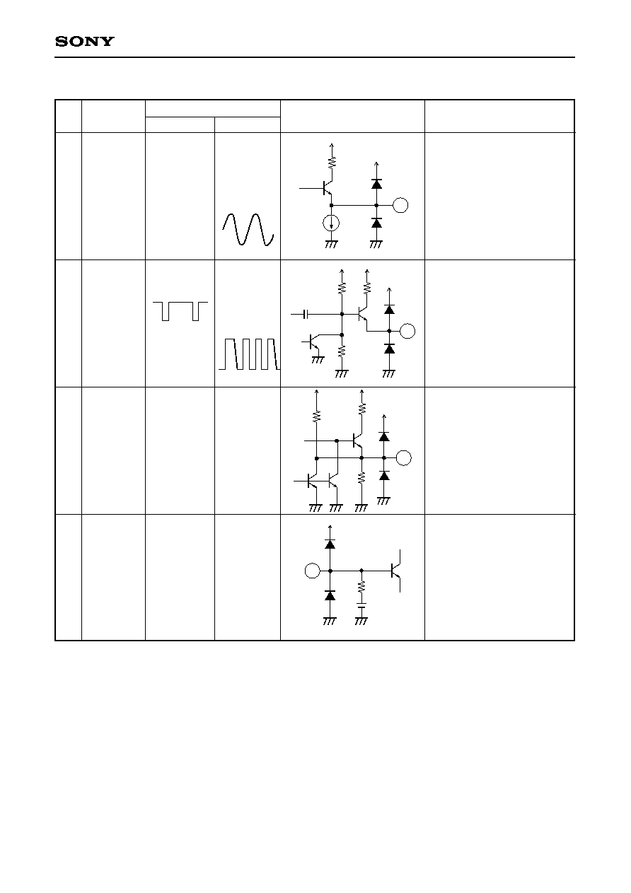
Input Signal
Signal
Input signal waveform
Signal
source
a
b
c
d
e
f
g
h
SG3
SG5-2
SG19
SG41
SG45
SG53
SG5-1
SG5-1
SG30
SG32
SG30
SG30
SG30
SG30
Frequency f (Hz)
Amplitude
V (mVp-p)
100% white
SYNC 0dB
357mV
143mV
1.5µsec
1H
63.5µsec
=
4.6µsec
4.5µsec
SYNC ≠6dB
71.5mV
SYNC +6dB
286mV
100% white
SYNC ≠6dB
357mV
71.5mV
0.4µsec
4.6µsec
210mVp-p
3.58MHz
SYNC 0dB With color burst
2.2µsec
143mV
141% white
SYNC 0dB
504mV
143mV
Frequency f (Hz)
50% white
Overlapping sine wave
SYNC 0dB
178.5mV
Sine wave
amplitude
357mVp-p
143mV
Signal
Input signal waveform
Signal
source
i
j
k
l
m
n
o
SG53
SG53
SG45
SG24
SG53
SG45
SG46
Burst signal V
B
(3.58MHz/143mVp-p)
Chroma signal V
C
(fHz/VmVp-p)
90∞
0∞
90∞
90∞ phase shift
f(Hz)/V(mVp-p)
◊
100 = 35%
V in MAX ≠ V in MIN
V in MAX + V in MIN
V in MAX
V in MIN
fsc/143mVp-p: 60Hz, 35% AM modulated
Burst signal V
B
(743kHz/200mVp-p)
PBC RF signal
Chroma signal (fHz/200mVp-p)
10m sec
10m sec
1.4V
0V
f(Hz)/V(mVp-p)
180∞
0∞
180∞ phase inversion
180∞
4.7µsec
1H(NTSC)63.56µsec: 15.734kHz
2.5V
0V
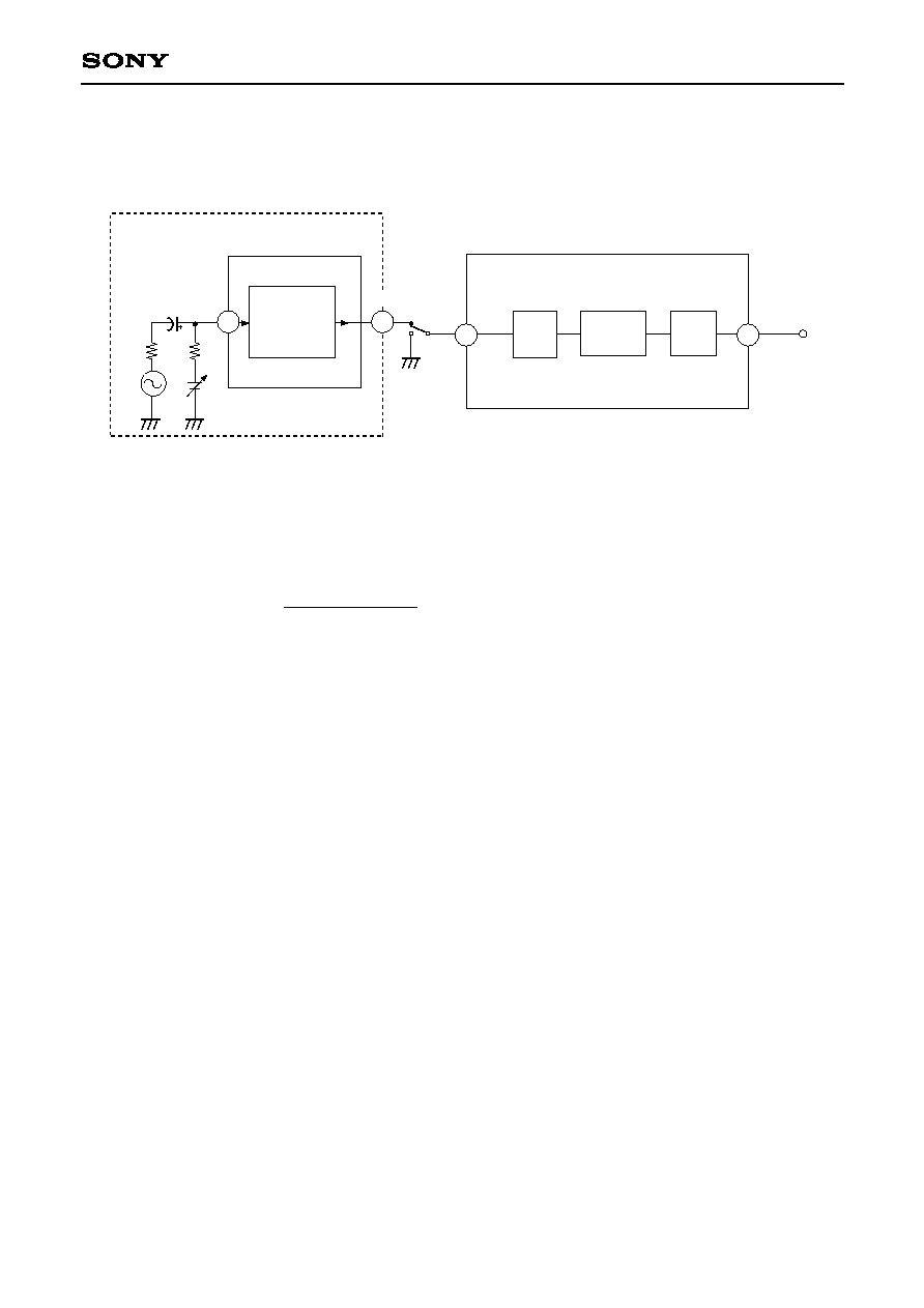
--28--
CXA1810AQ/AR
Detailed Explanation of Measurement Method
(1) DEMOD LPF frequency characteristics measurement
Using the CXA1207A as a modulator, the configuration for SG41 is shown below.
First, without inputting SG54, adjust V
CAR
so that the Y RF OUT (Pin 43) output frequency of the
CXA1207A is 5MHz. Use V
CARO
for the V
CAR
voltage. Next, apply V
CARO
+ 500mV, measure the Y RF
OUT (Pin 43) output frequency fo of the CXA1207A, and then calculate the MOD gain using the following
equation.
GMOD =
fo (MHz)≠5 (MHz)
500 (mV)
The compensation values are derived from GMOD and from GDEMOD1 and GDEMOD2 of measurement
Nos. 57 and 59.
Standard mode compensation value : G
C1
= 20log [G
MOD
(MHz/mV)
◊
G
DEMOD1
(mV/MHz)]
Hi-8 mode compensation value :
G
C2
= 20log [G
MOD
(MHz/mV)
◊
G
DEMOD2
(mV/MHz)]
Next, in order to set the SG41 carrier frequency, adjust V
CAR
so that the Y RF OUT (Pin 43) output of the
CXA1207A in standard mode is 4.8MHz and in Hi-8 mode is 6.7MHz.
In the above state, measure the I/O gain for the SG54 (200mVp-p/300kHz) input and P7 (Pin 7 DEMOD
OUT), with the gain for standard mode being G
LPF10
and for Hi-8 mode G
LPF20
.
Using these measured values and compensation values, the low frequency gain for DEMOD LPF is
determined using the following equations:
Standard mode :
G
LPF11
= G
LPF10
- G
C1
(dB)
Hi-8 mode :
G
LPF21
= G
LPF20
- G
C2
(dB)
CXA1207A
FM
MOD
REC MODE
SW41
YRFIN
LIM
DEMOD
LPF
CXA1810A to be measured
CAR
1µ
4700
4700
SG54
V
CAR
(SG41)
YRFOUT
54
43
41
7
P7
DEMOD
OUT
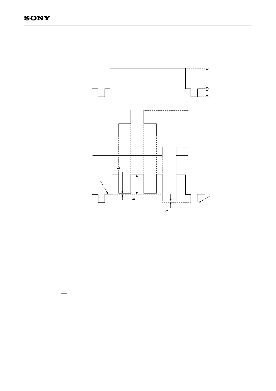
--29--
CXA1810AQ/AR
(2) DDS measurement
When a pulse with the following timing is input, the output from P34 (Pin 34 Y OUT) becomes as shown
below; measures each DC difference.
(3) Measurement of gain difference between PB ACC channels
The ACC amplifier in the CXA1810A has a built-in 4-channel time constants, and those time constants can
be switched by SWP (Pin 46) input. In addition, in NTSC playback chroma signal processing, PI return
occurs in the SWP (Pin 46) input for Low interval. In this measurement, the signal k, that is phase-inverted
each 1H, is input to PBC IN (Pin 45) for the Low interval of SWP; the continuous wave of the signal is
input for the High interval of SWP.
In this case, measure each channel level V
1
, V
2
, V
3
, and V
4
of output P63 (Pin 63 C OUT) and calculate
the gain difference between channels using the following equations:
GCH12
=
V
2
V
1
GCH13
=
V
3
V
1
GCH14
=
V
4
V
1
357mV
143mV
3V
1.5V
0V
0V
5V
V
VOB
V
VOW
V
JOGV
SG26 (Pin 26 DDS/MASK input)
SG31 (Pin 31 RECL/JVD input)
P34 (Pin 34 Y OUT) output
Pedestal level reference
Sync tip level reference
SG30 (Pin 30 VIN1 input)
100% white
Y signal

--30--
CXA1810AQ/AR
S
I
G
N
A
L
a
S
I
G
N
A
L
k
PB C
LPF
ACC
AMP
ACC
DET
ACC
CH HOLD
V46
SG46
(SG45)
63
45
46
CXA1810A to be measured
SWP
C OUT
P63
PB C IN
C32
100p
SW45
SIGNAL a
10m sec
10m sec
SIGNAL k
SG46 (Pin 46 SWP input)
SG45 (Pin 45 PB C IN input)
200mVp-p/743kHz
P63 (Pin 63 C OUT output)
V
1
V
2
V
3
V
4
SIGNAL a
SIGNAL k
P8 (Pin 8 REC C OUT output)
SG53 (Pin 53 EXT CIN input)
V
INMIN
V
INMAX
V
0MIN
V
0MAX
F
ACC
=
20log V
OMAX
/V
OMIN
(4) High-speed ACC compression ratio measurement
Measure the high-speed ACC compression ratio in JOG mode by inputting a modulation wave as shown
below.

--31--
CXA1810AQ/AR
BUS DECODER Mode Condition Table for Measuring Electrical Characteristics
(
Blanks indicate Low)
TEST2
TEST1
SYNC OFF
CORRE H
SHP THROU
ACK OFF
FBC L2
C SEL
DC2
DC1
C MUTE OFF
PAL
CAMREC
PS
Yd
NCLP2
NCLP1
NCL2
NCL1
CFL2
CFL1
E
FBC L1
JOG
EDIT
CCIR
WCCD
MUTE
Video AGC
INSEL
S
PB
H
H
H
H
H
H
H
H
H
H
H
H
H
H
H
H
H
H
H
H
H
H
H
H
H
H
H
H
H
H
H
H
H
H
H
H
H
H
H
H
H
H
H
H
H
H
H
H
H
H
H
H
H
H
H
H
H
H
H
H
H
H
H
H
H
H
H
H
H
H
H
H
H
H
H
Mode
condition
A
B
C
D
E
F
G
H
I
J
1
J
2
J
3
J
4
K
L
1
L
2
L
3
L
4
L
5
M
N
O
P
Q
R
S
1
S
2
S
3
S
4
T
U
V
1
V
2
V
3
V
4
Description
Composite REC (Video AGC OFF)
Composite REC (Video AGC ON)
Separate REC
Composite REC power save
Separate REC power save
Normal PB
Y comb OUT f characteristics
Y pre-emphasis characteristics
Hi-8 modulator characteristics
PB Y comb filter ATT level
PB sharpness characteristics
Noise canceler frequency
characteristics
Hi-8 demodulation characteristics
C OUT level (REC)
C OUT level (S/REC)
ACC, BE, CE characteristics
REC C measurement (NTSC)
REC C measurement (PAL)
REC AFC pull-in range
(NTSC)
REC AFC pull-in range
(PAL)
PB C system measurement
High-speed ACC compression ratio
PB APC pull-in range
(NTSC)
PB APC pull-in range
(PAL)

--32--
CXA1810AQ/AR
Precautions Concerning Measurements (Refer to Electrical Characteristics Measurement Circuit).
1. Start measurements after making the following adjustments.
1) Recording level (video AGC) adjustment
With the SW conditions (SW30: on) and the mode conditions: B the same as for measurement Nos.
11 to 13, adjust V31 so that the P34 (Pin 34 Y OUT) output is 500mVp-p when signal b (100% white,
500mVp-p Y signal) is input from SG30.
2) CAR adjustment (normal)
With the SW conditions at the initial settings and the mode conditions: A, adjust V44 so that the
frequency of the P39 (Pin 39 Y RF OUT) output is 4.2MHz.
3) Chroma emphasis adjustment
With the SW conditions (SW24-1, SW24-2, SW53: on), and the mode conditions: P the same as for
measurement Nos. 84 to 89, adjust V1 so that the signal level for the chroma interval of the P8 (Pin 8
REC C OUT) output is at a minimum when signal l is input from SG24 and signal i is input from SG53.
(chroma interval 3.58MHz/99.3mVp-p)
2. Although no input conditions are indicated for C measurement Nos. 80 to 126, signal l is input from SG24.
Unless otherwise specified in the input conditions, the frequency for SG24 is 15.734kHz.
3. Note that in regards to the measurements shown below, the characteristics change depending on the
floating capacitance.
1)
White/dark clipping level
2)
Pre-emphasis characteristics
3)
REC APC pull-in range
4. When taking measurements, use metal film resistors with an allowable deviation of 1% for R1, R2, R3, and
R5, and use temperature compensation CH types for C1, C2, C3, and C4.
--33--
CXA1810AQ/AR
BUS DECODER
1) Data contents
1
TEST2
H
L
2
TEST1
H
L
3
SYNC
H
OFF
L
4
CORRE H
H
L
5
SHP
H
THRU
L
6
ACK OFF
H
L
7
F.B.C. L2
(Feedback
Comb)
8
C SEL
H
L
TEST2 mode
1) Outputs VCO OUT signal to BF VCO
(Pin 62).
2) Outputs white/dark-clipped Y
signal to Y REF OUT (Pin 39).
Normal
TEST1 mode
1) Cuts APC loop and inputs signal from
CAM FSC SHP (Pin 60) to VCO OUT.
2) During REC, outputs burst emphasis
output to REC C OUT (Pin 8).
3) For the PB chroma feedback comb
measurement, inputs signal from EXT
C IN (pin 53) to the comb block without
passing it through PB CONV.
Normal
Sync separation does not operate.
(External input to COMP SYNC (Pin 24) is
possible).
Normal
Fixes the correlation pulse High so that
there is always correlation.
Detects correlation.
Sharpness block through (does not pass
through fsc Trap, Sharpness, LPF and
EQ)
Normal
ACK SW does not operate according to
ACK DET; always fixed to color mode.
ACK operation is performed according to
ACK DET.
Switches the feedback amount of the FBC
(feedback comb).
Refer to Table 1.
During recording, the signal input to EXT
C IN (Pin 53) is input directly to the ACC
amplifier.
Normal
bit
No.
Mode
Content
9
DC 2
(Dark Clip)
10
DC 1
11
C MUTE
H
OFF
L
12
PAL
H
L
13
CAM REC
H
L
14
PS
H
(Power
Save)
L
15
Yd
H
L
The dark clipping level is switched as
shown below. (when white clipping is
235% and WDC (Pin 27) is left open)
(Unit : %)
Switches the amount of the dark clipping
level offset to the white clipping level,
which can be varied in steps of 10%.
Disables MUTE for the chroma signal by
the MASK signal.
Mutes the chroma signal by the MASK
signal.
PAL (chroma function)
NTSC
During recording, inputs fsc, locked to
burst, from CAM FSC SHP (Pin 60)
without performing APC with the input
chroma signal, and then performs
frequency conversion using this fsc.
Recordable rise time can be reduced to
0.2 seconds or less from power saving
mode with separate input.
Normal
1) S∑PS (31.S=Low)
Changes to power saving mode with
composite input. Power consumption:
140mW (V
CC
=4.75V)
2) S∑PS (31.S=High)
Changes to power saving mode with
separate input. Power
consumption:250mW (V
CC
=4.75V)
Normal
Performs Yd playback during playback.
Normal
High
Low
High
85
95
Low
105
115
DC 1
DC 2
bit
No.
Mode
Content

--34--
CXA1810AQ/AR
16
NCLP2
17
NCLP1
18
NCL2
19
NCL1
20
CFL2
21
CFL1
22
E
H
L
23
F.B.C. L1
24
JOG
H
L
25
EDIT
H
L
26
CCIR
H
L
27
W CCD
H
L
28
MUTE
H
L
During playback, switches the noise
canceler characteristics.
The typical value of PB Y comb filter
depth is switched as shown below.
(Low frequency: insignificant level input)
Hi-8 mode
Standard mode
Switches the feedback amount of the
chroma feedback comb.
Refer to Table 1.
1) High-speed ACC mode.
2) During playback, is not performed
dropout compensation.
Normal
EDIT mode
1) During recording, the chroma signal is
Y/C separated by the BPF only without
passing though the comb filter.
2) During playback, cuts the feedback
loop of chroma feedback comb.
3) During playback, makes the sharpness
characteristics flat.
Normal
For fsc = 4.43MHz
For fsc = 3.58MHz
For two CCD delay lines
For one CCD delay line
1) Mutes the Y and chroma signals.
2) Discharges the charge in the external
clamp capacitance for VIN1 (Pin 30)
and VIN2 (Pin 28) and in the external
capacitance for AGC TC1 (Pin 29).
Normal
bit
No.
Mode
Content
29
Video AGC
H
L
30
INSEL
H
(INput
L
SELection)
31
S
H
L
32
PB
H
L
Video AGC on
Video AGC off
Selects VIN2 (Pin 28) input.
Selects VIN1 (Pin 30) input.
For separate signals during recording.
For composite signals during recording.
Playback mode
Recording mode
bit
No.
Mode
Content
High
Low
High
≠10dB
≠6dB
Low
≠1.5dB
0dB
CFL1
CFL2
Table 1. Chroma Feedback Comb Loop Gain
F.B.C.L1
Low
High
F.B.C.
Low
0dB
+1.9dB
L2
High
+4.8dB
+6.7dB
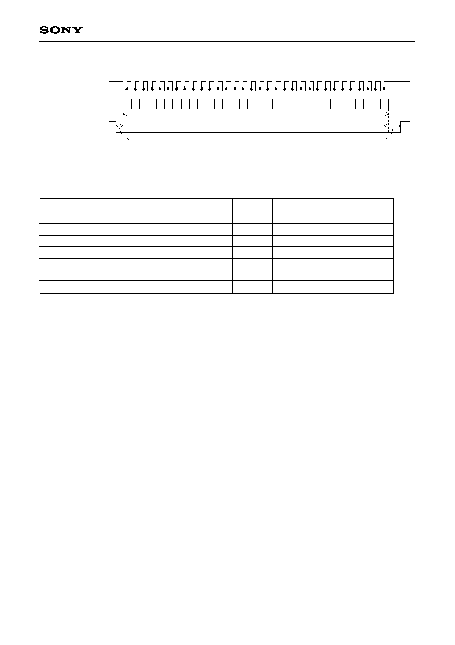
--35--
CXA1810AQ/AR
2) Timing chart
3) Input conditions
1
2
3
4
5
6
7
8
9 10 11 12 13 14 15 16 17 18 19
20 21 22 23 24 25 26 27 28 29 30 31 32
Pin 49 CK (Clock)
Pin 48 SI (Signal In)
Pin 47 CS(Chip Select)
Over 2µs
For CXA1810A data
Over 2µs
Latch
Input high level for Pins 47, 48, and 49
Input low level for Pins 47, 48, and 49
Clock frequency
Setup time
Hold time
CS fall time to SI start time
Final CK rise time to CS rise time
V
B-H
2.0
V
V
B-L
1.0
V
f
CK
1.3
MHz
t
SU
400
nsec
t
HLD
400
nsec
t
1
2
µsec
t
2
2
µsec
Item
Symbol
Min.
Typ.
Max.
Unit
--36--
CXA1810AQ/AR
BUS DECODER Mode Condition Table (NTSC)
Note)
"
" Don't care. In addition, select for the blank SHP THRU/W CCD column based on the system
configuration; for other blanks according to the characteristics.
TEST2
TEST1
SYNC OFF
CORRE H
SHP THROU
ACK OFF
FBC L2
C SEL
DC2
DC1
C MUTE OFF
PAL
CAMREC
PS
Yd
NCLP2
CAMERA
VCR
STANDBY
REC
EDIT
SEARCH
REC
PB
S
RCA
Normal
PB
EDIT
Hi-8
Standard
Hi-8
Standard
Hi-8
Standard
Hi-8
Standard
Hi-8
Standard
Hi-8
Standard
Hi-8
Standard
SP
LP
SP
LP
SP
LP
SP
LP
L L L L
L
L
L L H H L
L L L L
L
L
L L H H L
L L L L
L
L
L L H L L
L L L L
L
L
L L H L L
L L L L
L
L
L L L L L
L L L L
L
L
L L L L L
L L L L
L
L
L L L L L
L L L L
L
L
L L L L L
L L L L
L
L
L L L L L
L L L L
L
L
L L L L L
L L L L
L
L L L L L
L L L L
L
L L L L L
L L L L
L
L L L L L
L L L L
L
L L L L L
L L L L
L
L L L L L
L L L L
L
L L L L L
L L L L
L
L L L L L
L L L L
L
L L L L L
NCLP1
NCL2
NCL1
CFL2
CFL1
E
FBCL1
JOG
EDIT
CCIR
WCCD
MUTE
Video AGC
INSEL
S
PB
CAMERA
VCR
STANDBY
REC
EDIT
SEARCH
REC
PB
S
RCA
Normal
PB
EDIT
Hi-8
Standard
Hi-8
Standard
Hi-8
Standard
Hi-8
Standard
Hi-8
Standard
Hi-8
Standard
Hi-8
Standard
SP
LP
SP
LP
SP
LP
SP
LP
H
L L L
L H H H L
L
L L L
L H H H L
H
L L L
L H H H L
L
L L L
L H H H L
H
H H L H L
H
L
H H L
L
H
H
L L L
L H H H L
L
L L L
L H H H L
H
L L L
L H L L L
L
L L L
L H L L L
H
L L L H L
H
H
L L L H L
H
L
L L L
L
H
L
L L L
L
H
H
L H L H L
H
H
L H L H L
H
L
L H L
L
H
L
L H L
L
H
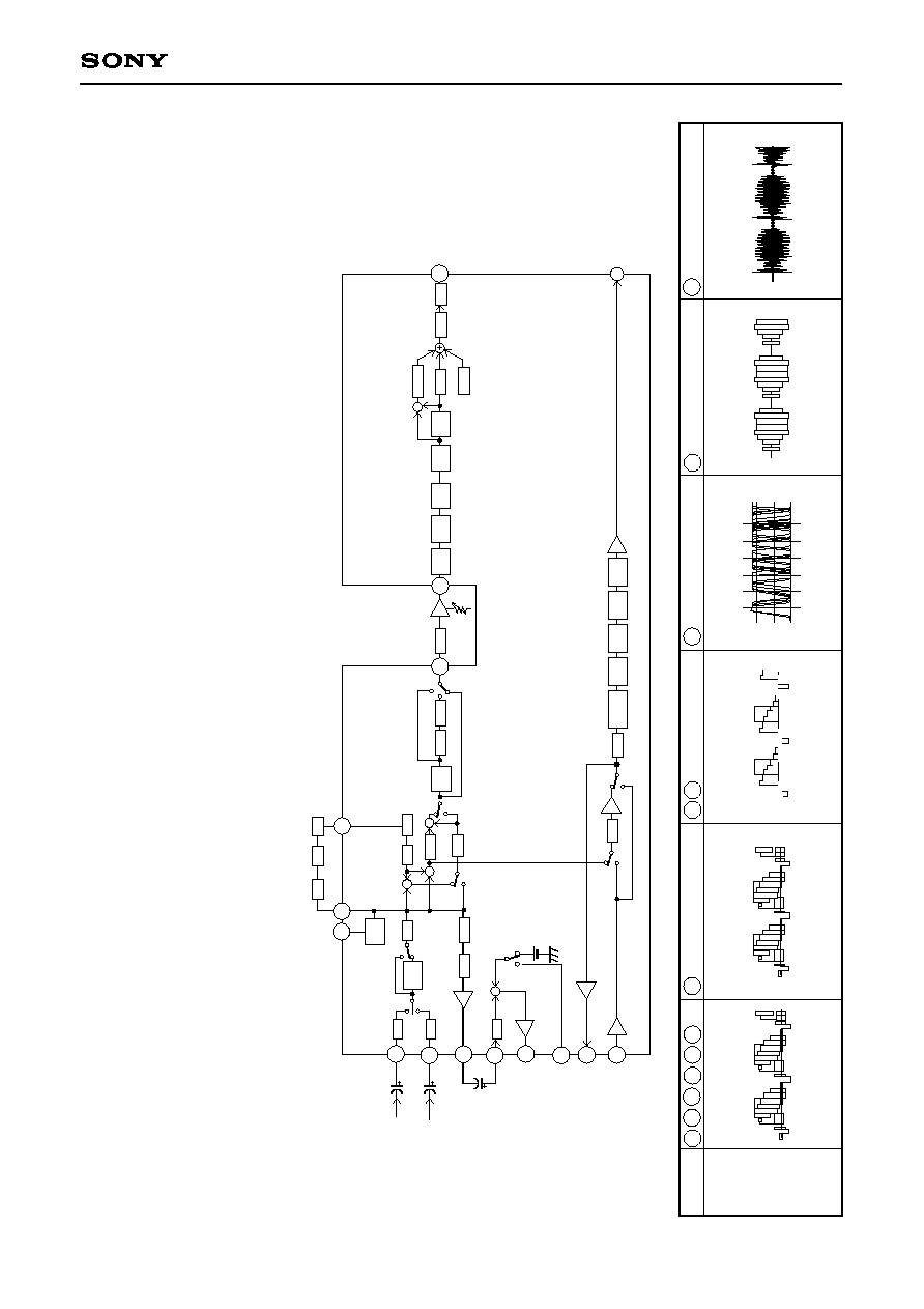
--37--
CXA1810AQ/AR
Description of Operation
1.
Signal path during composite recording
Composite signals input from VIN1 (Pin 30) and VIN2 (Pin 28) are selected by mode INSEL, passed through the VIDEO AGC, and Y/C
separated by the
comb filter. The Y signal is output to Y COMB OUT (Pin 14). Next, level adjustment is performed externally and then the signa
l is input to EMPH IN (Pin
5), after which hard clipping, emphasis, white/dark clipping, and FM modulation are performed and then the signal is output fro
m Y RF OUT (Pin 39). In
addition, the Y OUT (Pin 34) signal is input to Y IN (Pin 32), and then the monitor signal is output from VIDEO OUT (Pin 36).
On the other hand, Y/C-separated C signal passes through the BPF and then along with being output to C OUT (Pin 63), the signal
is also passed through
ACC, chroma emphasis, and burst emphasis, low frequency converted, is passed though a LPF and then output from REC C OUT (Pin 8
).
L
I
M
M
O
D
Y
R
F
O
U
T
S
M
E
A
R
D
E
V
I
C
A
R
R
W
/
D
C
L
I
P
M
A
I
N
E
M
P
H
H
A
R
D
C
L
I
P
C
L
P
E
Q
T
R
A
P
L
P
F
V
C
A
E
Q
S
H
P
T
R
A
P
E
Q
C
L
P
S
Y
N
C
S
E
P
C
L
P
M
U
T
E
D
D
S
V
I
D
E
O
A
G
C
C
L
P
C
L
P
C
L
P
C
C
D
L
P
F
E
Q
.
D
L
I
N
1
D
L
O
U
T
1
V
I
N
1
V
I
N
2
Y
O
U
T
Y
I
N
V
I
D
E
O
O
U
T
B
U
R
S
T
E
M
P
H
C
I
N
C
O
U
T
E
X
T
C
I
N
B
P
F
A
C
C
C
H
R
O
M
A
E
M
P
H
R
E
C
C
O
N
V
R
E
C
C
L
P
F
A
C
K
S
W
R
E
C
C
O
U
T
C
O
M
P
S
Y
N
C
S
U
B
E
M
P
H
8
+
+
+
+
+
≠
+ +
+
≠
3
9
5
1
4
2
1
2
3
2
4
3
0
2
8
3
4
3
2
3
6
6
4
6
3
5
3
E
M
P
H
I
N
Y
C
O
M
B
O
U
T
Pin No.
28 30 34 32 23 21
Signal
waveform
36
14 5
0.5Vp-p
2.0Vp-p
0.5Vp-p
0.5Vp-p
0.32Vp-p
0.3Vp-p
39
63
8
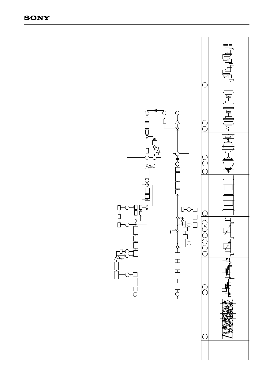
2.
Signal path during playback (W CCD)
The playback Y RF signal, after having passed though RF AGC and a soft limiter, is input to Y RF IN (Pin 41). After FM demodul
ation, the signal passes
through the LPF and is then output from DEMOD OUT (Pin 7). After the waveform is formed and the level is adjusted by an extern
al LPF, EQ, and
peaking amplifier, the signal is input to DE EMPH IN (Pin 10), after which clipping compensation, de-emphasis and HHS cancellat
ion are performed. Next,
cross talk cancellation is performed by a comb filter and then the signal is output from Y COMB OUT (Pin 14). After the wavefo
rm is formed and the level
is adjusted by an external EQ (LPF) and peaking amplifier, the signal is input to EMPH IN (Pin 5), where it passes through a no
ise canceler and is then
output from Y OUT (Pin 34).
On the other hand, the playback RF signal, after passing through AFM and ATF TRAP, is input to PBC IN (Pin 45), after which the
low-frequency C signal
is separated by the PBC LPF. Next, the playback C signal, which has undergone level control by the ACC and frequency conversio
n by PB CONV and
PBC BPF, is subjected to cross talk cancellation by the comb filter, and then after undergoing burst de-emphasis and chroma de-
emphasis, the signal is
output from C OUT (Pin 63).
By inputting the playback Y signal (Y
OUT (Pin 34) output) to Y IN (Pin 32) and the playback C signal (C OUT (Pin 63) output) to C IN (Pin 64), the Y/C
mixed signal is output from VIDEO OUT (Pin 36).
D
D
S
M
U
T
E
H
P
F
f
s
c
T
R
A
P
E
Q
S
H
P
H
H
S
C
A
N
C
E
L
M
A
I
N
D
E
E
M
C
L
I
P
C
O
M
P
H
P
F
E
Q
P
e
a
k
i
n
g
H
P
F
A
T
T
C
C
D
L
P
F
E
Q
V
C
A
B
P
F
B
U
R
S
T
D
E
E
M
C
H
R
O
M
A
D
E
E
M
A
C
K
S
W
C
L
P
C
L
P
L
P
F
E
Q
P
e
a
k
i
n
g
C
L
P
L
I
M
L
P
F
A
T
T
C
L
P
C
L
P
S
U
B
D
E
E
M
+
+
+
_
+
_
_
+
+
_
+
+
+
+
_
+
+
3
6
3
2
3
4
5
6
6
4
6
3
2
1
2
3
1
2
4
5
4
1
7
1
0
9
1
4
P
B
C
L
P
F
A
C
C
P
B
C
O
N
V
P
B
C
B
P
F
L
P
F
D
E
M
O
D
L
I
M
A
T
T
L
I
M
1
7
1
9
E
Q
L
P
F
C
C
D
V
C
A
_
L
P
F
Y
O
U
T
Y
I
N
V
I
D
E
O
O
U
T
E
M
P
H
I
N
N
C
T
C
I
N
Y
C
O
M
B
O
U
T
C
I
N
C
O
U
T
D
L
O
U
T
2
D
L
I
N
2
C
O
M
P
T
C
D
E
E
M
P
H
I
N
D
E
M
O
D
O
U
T
Y
R
F
I
N
P
B
C
I
N
C
T
R
A
P
D
L
O
U
T
1
D
L
I
N
1
Pin No.
41
Signal
waveform
7 10
17 19 14 5 34 32
45
12 ( 23 21 )
63 64
2Vp-p
36
0.2Vp-p
0.17Vp-p
0.5Vp-p
0.5Vp-p
0.3Vp-p
(Pins 23 and 21 are
with pseudo sync)
0.3Vp-p
--38--
CXA1810AQ/AR
--39--
CXA1810AQ/AR
3. REC LEVEL adjustment
The video signal input to VIN1 (Pin 30) and VIN2 (Pin 28) is selected by mode INSEL, and when mode
video AGC is High, the signal is passed through SYNC AGC and PEAK AGC and then is output from Y
OUT (Pin 34). The output level can be adjusted by applying an external DC bias (1.3 to 2.6V [Vcc =
4.75V]) to RECL/JVD (Pin 31). In the case of 100% white , 500mVp-p input, the following are the standard
characteristics.
4. MASK DDS
DDS/MASK (Pin 26) is the VOW (character level) signal and the VOB (character background) and
masking timing pulse input pin. The threshold value for raw signal and VOB/masking is 1.1V, and the
threshold value for VOB/masking and VOW is 2.0V (when Vcc = 4.75V). In addition, the VOW replacement
signal level can be varied within the range of the DC level (2.3V to 3.0V) for this pin; those standard
characteristics are shown below.
3.0
400
1.0
500
(mVp-p)
1.5
2.0
2.5
Y
O
U
T
(
P
i
n
3
4
)
o
u
t
p
u
t
l
e
v
e
l
REC L/JVD (Pin 31) control DC (V)
600
3.0
60
2.0
80
(%)
2.5
MASK/DDS (Pin 26) DC level
Y
O
U
T
(
P
i
n
3
4
)
r
e
p
l
a
c
e
m
e
n
t
s
i
g
n
a
l
l
u
m
i
n
a
n
c
e
l
e
v
e
l
( V
CC
=4.75V)
100

--40--
CXA1810AQ/AR
5. White/dark clipping adjustment
The white/dark clipping levels can be varied connectedly using the DC level of WDC (Pin 27). In addition,
the dark clipping level is switched independently by DC1 and DC2 of the mode. The standard
characteristics of standard/Hi-8 after Y pre-emphasis are shown below. (when 100% white, 500mVp-p
input to Pin 5 EMPH IN)
1) Standard mode
2) Hi-8 mode
2.4
≠100
2.6
0
200
(%)
2.5
100
WDC DC (Pin 27) level (V)
Y
R
F
O
U
T
(
P
i
n
3
9
)
w
h
i
t
e
/
d
a
r
k
c
l
i
p
p
i
n
g
l
e
v
e
l
(
m
o
d
e
t
e
s
t
2
:
H
i
g
h
)
White Clip Level
100%
Dark Clip Level
(DC1, DC2)
(H, H)
(L, H)
(H, L)
(L, L)
when open
(VG
1
=2.05V)
2.4
2.6
0
200
(%)
2.5
100
WDC DC (Pin 27) level (V)
≠100
Y
R
F
O
U
T
(
P
i
n
3
9
)
w
h
i
t
e
/
d
a
r
k
c
l
i
p
p
i
n
g
l
e
v
e
l
(
m
o
d
e
t
e
s
t
2
:
H
i
g
h
)
White Clip Level
Dark Clip Level
(DC1, DC2)
(H, H)
(L, H)
(H, L)
(L, L)
100%
(VG
1
=2.05V)

--41--
CXA1810AQ/AR
6. Carrier/deviation adjustment
The Y FM modulation carrier frequency is adjusted by applying an external DC bias to CARR CONT (Pin
44). When carrier adjustment is performed, gm
1
and gm
2
, the deviation/smear gain, change in proportion
to I
XCAR
at the same time. This results in the FM modulator sensitivity being roughly adjusted for the Dev
IN/Sme IN signal level. Fine adjustment of the deviation frequency is accomplished by the DC bias
applied to DEV CONT (Pin 43).
I
XCAR
Carr
Cont
FM
Mod
LIM
I
XDEV
I
XSME
Dev IN
Sme IN
Smear
Cont
Dev
Cont
DEV CONT
SMEAR
CONT
g
m1
gm1=K
1
I
XDEV
g
m2
gm2=K
2
I
XSME
43
42
39
44
CARR CONT
YRFOUT
--42--
CXA1810AQ/AR
6-1. Carrier frequency adjustment
The standard characteristics of carrier frequency for the CARR CONT (Pin 44) DC bias (1.8V to Vcc)
when bias was applied to EMPH IN (Pin 5) with VG1 are shown below.
5
5
1
6
7
(MHz)
2
3
4
(V
CC
=4.75V)
CARR CONT (Pin 44) DC level (V)
Y
R
F
O
U
T
(
P
i
n
3
9
)
c
a
r
r
i
e
r
f
r
e
q
u
e
n
c
y
(Hi-8 mode)
5
3
1
4
5
(MHz)
2
3
4
CARR CONT (Pin 44) DC level (V)
Y
R
F
O
U
T
(
P
i
n
3
9
)
c
a
r
r
i
e
r
f
r
e
q
u
e
n
c
y
(Standard mode)
(V
CC
=4.75V)
--43--
CXA1810AQ/AR
6-2. Deviation frequency adjustment
The standard characteristics of deviation frequency for the DEV CONT (Pin 43) DC bias (1.8V to Vcc)
when bias was applied to EMPH IN (Pin 5) with V
G1
+ 0.5V after carrier frequency adjustment are shown
below.
DEV CONT (Pin 44) DC level (V)
Y
R
F
O
U
T
(
P
i
n
3
9
)
d
e
v
i
a
t
i
o
n
f
r
e
q
u
e
n
c
y
5
1.5
1
2.5
2
3
4
2.0
(Hi-8 mode)
(MHz)
(V
CC
=4.75V)
DEV CONT (Pin 44) DC level (V)
Y
R
F
O
U
T
(
P
i
n
3
9
)
d
e
v
i
a
t
i
o
n
f
r
e
q
u
e
n
c
y
5
1.0
1
2.0
(MHz)
2
3
4
1.5
(Standard mode)
(V
CC
=4.75V)

--44--
CXA1810AQ/AR
7. Chroma emphasis fo adjustment
The center frequency of the chroma emphasis characteristics is adjusted by the DC bias (1.8V to 3.8V
[Vcc = 4.75V]) applied to CE CONT (Pin 1). The standard characteristics of center frequency for the CE
CONT (Pin 1) DC level are shown below.
8. ACC/ACK standard characteristics
R
E
C
C
O
U
T
(
P
i
n
8
)
(
m
o
d
e
t
e
s
t
1
:
H
i
g
h
)
/
c
h
r
o
m
a
e
m
p
h
a
s
i
s
f
o
4
≠100k
2
+100k
3
fsc
CE CONT (Pin 1) DC level (V)
(Hz)
(V
CC
=4.75V)
EXT C IN (Pin 53) input level
10
≠10
≠30
0
(dB)
0
≠5
≠20
≠10
R
E
C
C
O
U
T
(
P
i
n
8
)
o
u
t
p
u
t
l
e
v
e
l
(
0
d
B
o
u
t
p
u
t
f
o
r
1
4
3
m
V
i
n
p
u
t
)
(143mVp-p=0dB)
ACK OFF
ACK ON
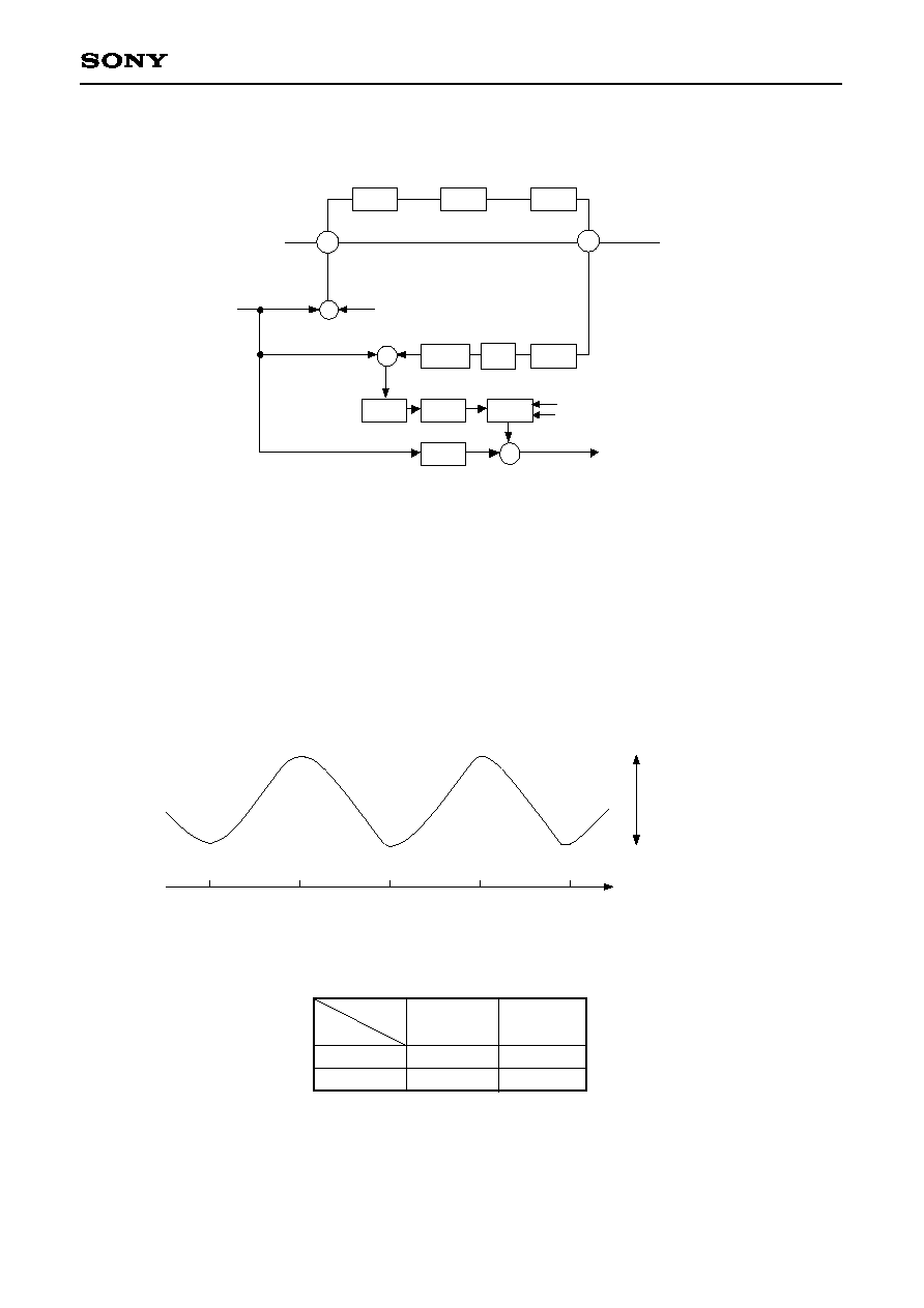
--45--
CXA1810AQ/AR
9. Y cross talk cancellation
De-emphasized playback Y signal is input to the comb block. By passing the differential component of the
nH signal and the (n+1) H signal through the limiter, the cross talk component, which is line
noncorrelation, is extracted. Cross talk cancellation is accomplished by subtracting this cross talk
component from the nH playback Y signal.
In addition, by switching modes CFL1 and CFL2, the comb depth characteristics of PBY cross talk
cancellation can be changed. The standard characteristics of comb depth for low frequency
(approximately 1MHz) and insignificant input level (MAIN EMPH TC (Pin 3) 7.9mVp-p = ≠30dB) input are
shown below.
CCD
LPF
EQ
DL OUT2
DL IN1
TRAP
LIM
ATT
CLAMP2
VCA2
EQ
CFL1
CFL2
OUT
DOC
TRAP
Playback Y
Playback C
C comb
+
≠
+
+
+
≠
19
23
(when using a single CCD)
64
H
65
H
PB Y Comb Depth
CFL1
High
Low
CFL2
High
≠10dB
≠6dB
Low
≠1.5dB
0dB

--46--
CXA1810AQ/AR
10. PB C cross talk cancellation
The playback C signal which passes through the BPF is input after frequency conversion. The feedback
chroma comb filter is configured as shown above.
By switching modes FBCL1 and FBCL2, the feedback loop gain from the Y comb is changed as shown
below.
Feedback loop gain
When the feedback loop gain is increased the S/N ratio can be improved, but note that color smear in the
vertical direction and transient response are both worsen.
CCD
EQ
ATT
CLAMP1
VCA1
HPF
FBCL1
FBCL2
OUT
NOCORRE + EDIT + BF
ACK ∑ BF
DL OUT1
DL IN1
Playback C signal
Playback Y or
pseudo-sync
C comb
Y comb
+
+
+
+
+
+
--
21
23
LPF
227
H
228
H
During editing
Feedback loop
gain is large
FBCL1
High
Low
FBCL2
High
6.7dB
4.8dB
Low
1.9dB
0dB
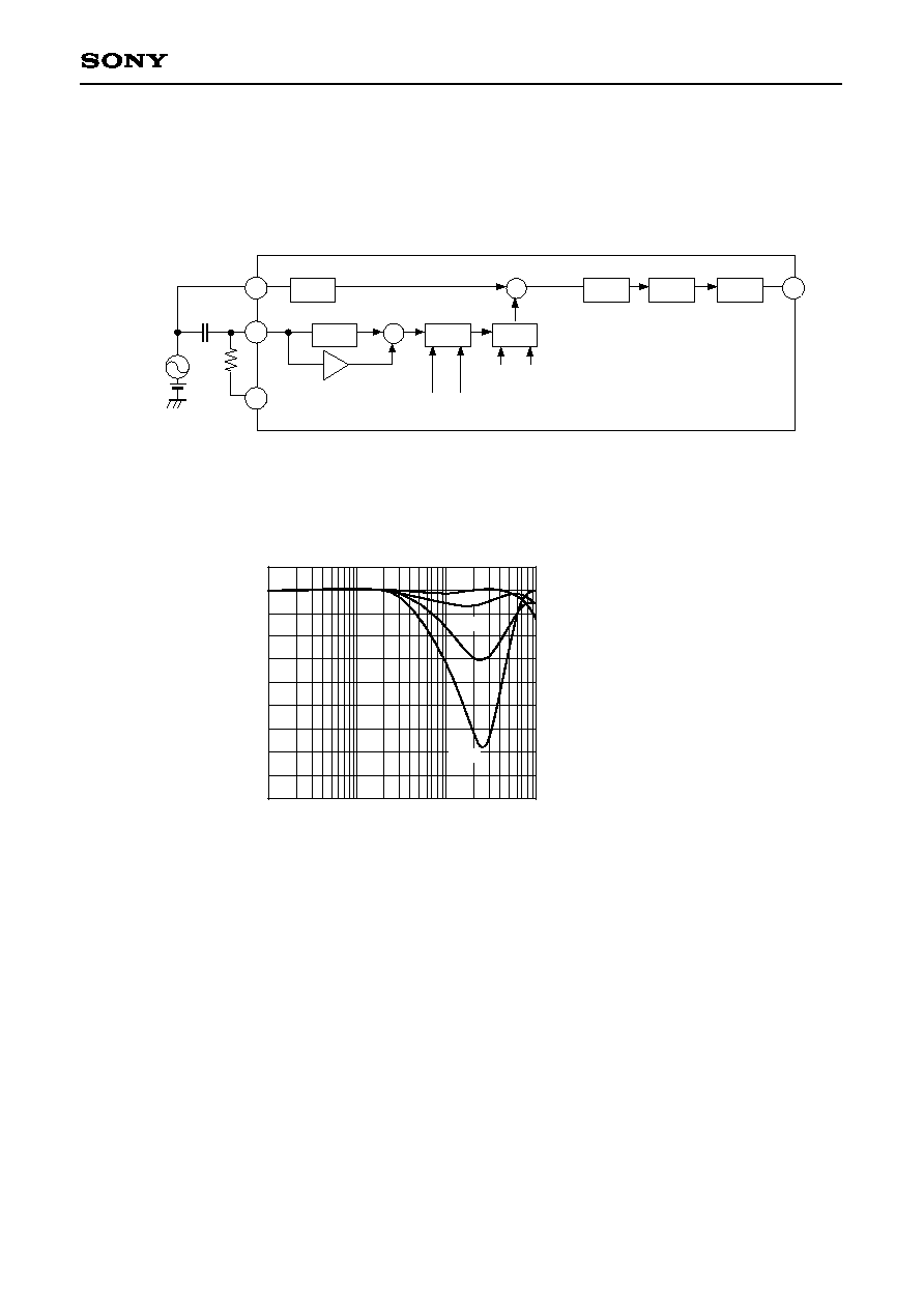
--47--
CXA1810AQ/AR
11. PB Y noise cancellation
When an external HPF is configured as shown below, the standard characteristics of PB Y noise
cancellation are as shown below, depending on the switching of input signal level, mode NCL1/2, external
HPF and mode NCLP1/2.
1) Changes in frequency characteristics due to the input level
CLP
MUTE
DDS
EMPH IN
CLP
LIM
LPF
ATT
NC TC IN
C
1k
VGI
2.37v
500mVp-p
=0dB
NCLP1 NCLP2
NCL1 NCL2
+
--
+
--
5
6
11
34
Y
O
U
T
(
P
i
n
3
4
)
/
E
M
P
H
I
N
(
P
i
n
5
)
I
/
O
g
a
i
n
0
≠2
10k
100k
1M
10M
(dB)
≠4
≠6
≠8
Input frequency (Hz)
≠30dB
≠10dB
≠20dB
≠3dB
NCL 1, 2 = H, H
NCLP 1, 2 = H, H
External HPF (1k
/82pF)
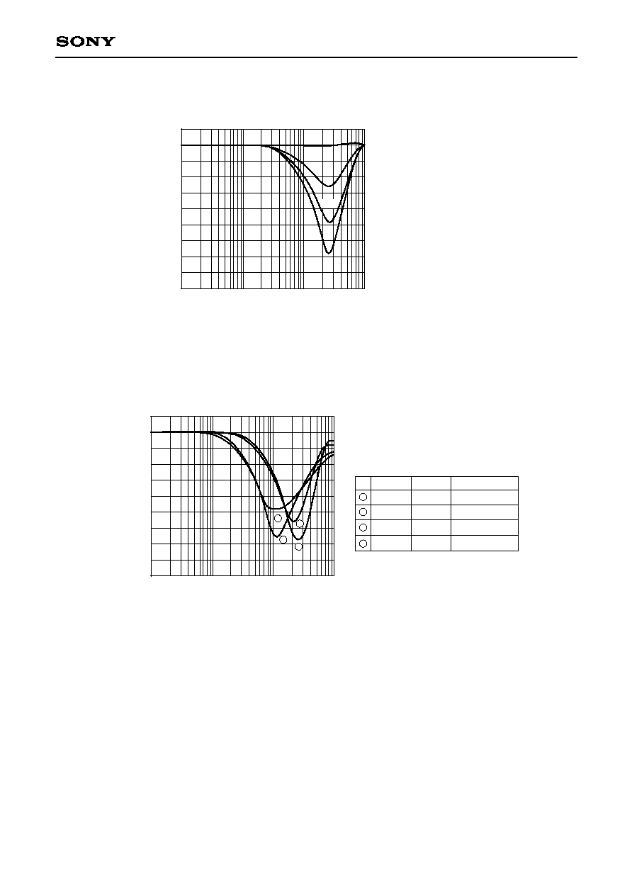
--48--
CXA1810AQ/AR
2) Changes in frequency characteristics due to switching of mode NCL1/2
3) Changes in frequency characteristics due to switching of external HPF and mode NCLP1/2
0
≠2
10k
L, L
100k
1M
10M
(dB)
≠4
≠6
≠8
H, L
H, H
L, H
Y
O
U
T
(
P
i
n
3
4
)
/
E
M
P
H
I
N
(
P
i
n
5
)
I
/
O
g
a
i
n
Input frequency (Hz)
NCLP 1, 2 = H, H
External HPF (1k
/82pF)
External HPF
1k
/220pF
1k
/220pF
1k
/82pF
1k
/82pF
0
≠2
10k
100k
1M
10M
(dB)
≠4
≠6
≠8
NCLP1
Low
High
Low
High
NCLP2
Low
Low
High
High
Y
O
U
T
(
P
i
n
3
4
)
/
E
M
P
H
I
N
(
P
i
n
5
)
I
/
O
g
a
i
n
Input frequency (Hz)
1
2
3
4
4
3
2
1
NCL 1, 2 = H, H
The following four conditions are compared:
--49--
CXA1810AQ/AR
12. BF OUT pulse
The timing for C.SYNC (Pin 24) output pulse and BF VCO (Pin 62) output pulse changes in each mode as
shown below. Note that the BPF delay time between C OUT (Pin 63) and C IN (Pin 64) during PAL
playback is designed to be 200nsec. In addition, the BF pulse width WdBF is constant.
TdBF
WdBF
PB
NTSC ∑ REC
PAL ∑ REC
: TdBF (PB)
: TdBF (PB) + 250nsec
: TdBF (PB) + 390nsec
--50--
CXA1810AQ/AR
Adjustment Procedure (Refer to Application Circuit.)
1. REC Y level adjustment
Mode :
REC, 29 video AGC = High
Input signal :
color bar 500mVp-p (Pin 30 V IN1)
Adjustment method :
When VIDEO OUT (Pin 36) is terminated with 75
, adjust RV105 (EE LEVEL) so
that the output is 1Vp-p.
2. Y/C separation adjustment
Mode:
REC, 5 SHP THRU = High
Input signal :
color bar 500mVp-p (Pin 30 V IN1)
Adjustment method :
Adjust RV110 (YC.SEP)
RV103 (COMB.ADJ)
RV110 (YC.SEP) in turn so that
the residual chroma component at Y COMB OUT (Pin 14) is minimum.
3. Emphasis input Y level adjustment
Mode :
REC
Input signal :
color bar 500mVp-p (Pin 30 V IN1)
Adjustment method :
Adjust RV112 (EMPH.Y.LEV) so that the Y signal level at EMPH IN (Pin 5) is
500mVp-p.
4. Y-FM carrier deviation adjustment
Mode :
REC, 22 E = Low (standard mode); E = High (Hi-8 mode)
Input signal :
100% white, 500mVp-p (Pin 30 V IN1)
Adjustment method :
While monitoring the Y RF OUT (Pin 39) signal with a spectrum analyzer, adjust
RV108 (CARR) so that the H SYNC spectrum (carrier) is 4.2MHz in standard mode
and 5.7MHz in Hi-8 mode, and adjust RV107 (DEV) so that the 100% white Y level
spectrum is 5.4MHz in standard mode and 7.7MHz in Hi-8 mode.
5. Chroma emphasis fo adjustment
Mode :
REC, 2 TEST1 = High
Input signal :
color bar 500mVp-p (Pin 30 V IN1)
Adjustment method :
Adjust RV102 (CEMPH) so that the level of the flat portion of the chroma signal
after burst emphasis output to REC C OUT (Pin 8) is minimum.
6. PB Y level 1 adjustment
Mode :
PB, 27 W CCD = Low (when using one CCD delay line)
W CCD = High (when using two CCD delay lines)
Input signals :
PB Y RF 200mVp-p (Pin 41 Y RF IN)
Adjustment method :
Adjust RV111 (PB.Y.LEV1) so that (when using one CCD delay line) DL IN 1 (Pin
23) or (when using two CCD delay lines) DL IN 2 (Pin 17) is 500mVp-p respectively.
7. PB Y level 2 adjustment
Mode :
PB
Input signal :
PB Y RF 200mVp-p (Pin 41 Y RF IN)
Adjustment method :
When VIDEO OUT (Pin 36) is terminated with 75
, adjust RV113 (PB.Y.LEV2) so
that the output is 1Vp-p.
Note on Operation
∑ I REF (Pin 55) resistance 18k determines the reference current. Employ a metallic film resistance and of
allowable difference ±1%.
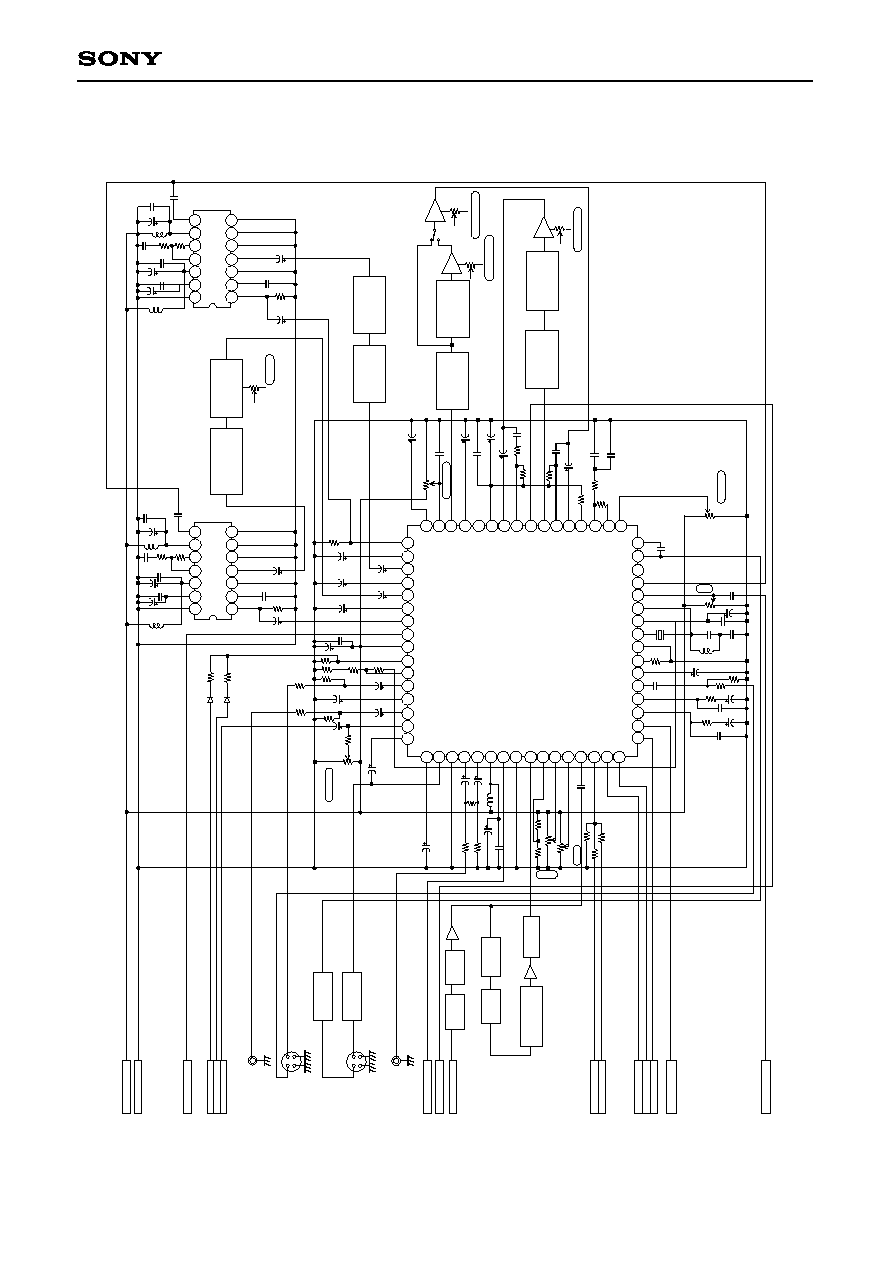
--51--
CXA1810AQ/AR
Application Circuit
(NTSC Hi-8 mode)
C
39
C2
05
C
1
1
0
R
1
3
1
1
k
1k
R1
11
R
1
0
2
1
0
k
2
2
0
C
1
0
4
DE
V
L
P
F
R
F
A
G
C
C
T
R
A
P
S
O
F
T
L
I
M
I
T
E
R
A
F
M
T
R
A
P
A
T
F
T
R
A
P
Y
B
U
F
F
E
R
C
B
U
F
F
E
R
L2
01
C2
04
3.3
0.0
1
C2
06
3.3
C2
07
0.0
1
R2
02
82
k
1k
R2
03
C
20
8
0.1
L2
02
10
µ
C2
09
3.3
C2
10
0.0
1
C
2
1
1
0
.
0
1
R V
11
0
Y
C
S
E
P
R
1
1
5
R
1
1
6
R1
12
39
R1
13
39
R V
10
5
47
k
R
1
1
0
4
7
k
C1
11
10
39
C1
13
10
R1
14
39
0
.
4
7
C1
12
0.4
7
C1
14
0.4
7
R1
20
C1
15
10
C1
16
0.0
1
C1
17
10
C1
19
3.3
C1
18
10
C1
20
10
C1
21
3.3
C2
01
1
R2
01
1M
C2
02
0.0
1
C2
03
10
C
1
3
0
1
0
R
V
1
0
3
4
7
k
C
1
3
1
0
.
0
1
C
1
3
3
0
.
0
1
C
1
3
2
1
0
C
1
3
4
1
0
C
1
3
5
4
7
C
1
3
6
4
7
0
p
R
1
3
0
1
k
1
k
R
1
3
2
C
1
3
7
8
2
p
C
1
3
8
0
.
4
7
R
1
1
3
3
3
0
0
R
1
3
4
3
9
0
C
1
3
9
1
5
0
p
C
1
4
0
1
5
0
p
R1
35
1.2
k
C
1
5
0
1
0
0
0
p
R V
10
2
47
k
C1
51
0.0
1
R V
12
0
47
k
C1
52
10
C1
53
0.0
1
C1
55
82
p
C1
54
0.0
1
L1
50
R1
50
18
k
C1
57
10
00
p
C1
56
1
R1
51
R1
52
R1
53
56
00
C1
58
0.6
8
C1
59
0.0
22
R1
54
68
00
C1
60
C1
61
1
33
0p
R
1
0
1
1
0
k
R
1
0
3
1
0
k
R
V
1
0
8
4
7
k
R
1
5
6
C
1
0
1
0
.
0
1
C
1
0
2
1
0
L
1
0
1
4
7
µ
C
1
0
5
0
.
2
2
R
1
0
6
6
8
R
1
0
4
1
k
R1
05
C
1
0
3
4
.
7
C
E
M
P
H
SH
P
XT
A
L
C
O
M
B
A
D
J
R V
11
3
R V
11
2
R V
11
1
D
1
1
1
D
1
1
0
C
C
D
O
U
T
L
P
F
Y
/
C
S
E
P
E
Q
P
B
Y
E
Q
D
E
M
O
D
O
U
T
E
Q
R
E
G
4
.
7
5
V
G
N
D
C
S
Y
N
C
D
D
S
M
A
S
K
J
O
G
V
D
R
E
C
Y
R
F
R
E
C
C
R
F
P
B
R
F
H
C
H
G
V
A
S
W
P
C
S
S
I
C
K
D
O
P
C
A
M
F
S
C
V
I
D
E
O
I
N
Y
S
I
N
C
Y
S
O
U
T
V
I
D
E
O
O
U
T
P
B
C
X
L
5
5
0
2
E
E
L
E
V
E
L
C
X
A
1
8
1
0
A
R
C
A
R
R
C
1
0
6
1
0
0
p
P
B
Y
L
E
V
1
P
B
Y
L
E
V
2
E
M
P
H
Y
L
E
V
R
1
5
5
4
7
k
24
23
22
21
20
19
18
17
31
30
29
28
26
32
25
33
34
35
36
37
38
39
40
41
42
43
44
45
46
47
48
4
9
5
0
5
1
5
2
5
3
5
4
5
5
5
6
5
7
5
8
5
9
6
0
6
4
6
3
6
2
6
1
16
15
14
9
11
12
13
8
7
6
5
4
3
2
1
10
7
6
5
4
3
2
1
1
4
9
1
1
1
2
1
3
8
1
0
VS
S
A
B
V
D
D
V
CO
IN
P
CO
UT
V
D
D
C
LK
SIG
IN
I/
01
I/
02
O
UT
V
SS
V
SS
V
CO
O U
T
39
22
µ
R
E
C
R
V
1
0
7
R1
21
2.2
k
C
2
3
1
C
X
L
5
5
0
2
6
5
4
3
2
1
VS
S
A
B
V
D
D
V
CO
IN
P
CO
UT
V
D
D
C
LK
SIG
IN
I/
01
I/
02
O
UT
V
SS
V
SS
V
CO
O U
T
7
R2
21
C2
22
C2
21
1
1M
0.0
1
C2
23
10
0
.
0
1
C2
30
0.0
1
C2
29
3.3
L2
22
R2
22
82
k
R2
23
1k
C2
28
0.1
9
1
1
8
1
4
1
2
1
3
C2
26
3.3
C2
25
L2
21
3.3
C2
24
0.0
1
C2
27
0.0
1
1
0
C
C
D
O
U
T
L
P
F
E
Q
Y
C
O
M
B
O
U
T
L
P
F
D
E
M
O
D
O
U
T
L
P
F
R1
17
R1
18
R1
19
27
10
µ
10
µ
10
µ
Application circuits shown are typical examples illustrating the operation of the devices. Sony cannot assume responsibility fo
r
any problems arising out of the use of these circuits or for any infringement of third party patent and other right due to same
.

--52--
CXA1810AQ/AR
Application Circuit
(PAL Hi-8 mode)
R V
12
0
4
.
7
R
1
3
0
0
.
4
7
39
R
E
G
4
.
7
5
V
R V
11
0
1
6
1
5
1
4
1
3
2
3
2
2
2
1
2
0
1
9
1
8
1
7
9
1
1
1
2
8
7
6
5
4
3
2
1
1
0
R
F
A
G
C
C
T
R
A
P
S
O
F
T
L
I
M
I
T
E
R
A
F
M
T
R
A
P
A
T
F
T
R
A
P
Y
B
U
F
F
E
R
C
B
U
F
F
E
R
R
1
0
2
1
0
k
R
1
0
1
1
0
k
R
1
0
3
1
0
k
R
V
1
0
8
4
7
k
C
1
0
1
0
.
0
1
C
1
0
2
1
0
L
1
0
1
4
7
µ
C
1
0
5
0
.
2
2
R
1
0
6
6
8
R
1
0
4
1
k
R1
05
1k
C
1
0
4
2
2
0
C
1
0
3
C1
60
C1
51
0.0
1
C1
52
10
C1
53
0.0
1
R1
50
18
k
C1
57
10
00
p
C1
56
1
R1
51
R1
52
39
R1
53
C1
58
0.6
8
C1
59
0.0
22
R1
54
39
00
C1
61
1
68
00
p
SH
P
XT
A
L
C1
50
10
00
p
R V
10
2
47
k
C
E
M
P
H
C
1
3
0
1
0
R
V
1
0
3
4
7
k
C
1
3
1
0
.
0
1
C
1
3
3
0
.
0
1
C
1
3
2
1
0
C
1
3
4
1
0
C
1
3
5
4
7
C
1
3
6
4
7
0
p
1
k
R
1
3
1
1
k
R
1
3
2
1
k
C
1
3
7
8
2
p
C
1
3
8
R
1
3
3
3
3
0
0
R
1
3
4
3
9
0
C
1
3
9
1
5
0
p
C
1
4
0
1
5
0
p
R1
35
1.2
k
C
O
M
B
A
D
J
R1
22
39
R1
13
39
R V
10
5
47
k
R
1
1
0
4
7
k
C1
11
10
R1
12
39
C1
13
10
R1
14
R1
20
C
1
1
0
0
.
4
7
C1
12
0.4
7
C1
14
0.4
7
C1
15
10
C1
16
0.0
1
C1
17
10
C1
19
3.3
C1
18
10
C1
20
10
C1
21
3.3
C2
01
1
R2
01
1M
C
20
2
0.0
1
10
k
J
O
G
L2
01
C2
04
3.3
C2
05
0.0
1
C2
06
3.3
C2
07
0.0
1
R2
02
R
20
3 C
20
8
0.1
L2
02
C
2
0
9
3.3
C2
10
0.0
1
C2
11
0.0
1
R V
11
2
R V
11
3
R V
11
1
C
C
D
O
U
T
L
P
F
Y
/
C
S
E
P
E
Q
R
1
1
5
R
1
1
6
D
1
1
1
D
1
1
0
D
1
1
2
D
1
1
3
G
N
D
C
S
Y
N
C
D
D
S
R
E
C
Y
R
F
R
E
C
C
R
F
P
B
R
F
H
C
H
G
C
S
D
O
P
C
A
M
F
S
C
V
I
D
E
O
I
N
C
Y
S
I
N
C
Y
S
O
U
T
V
I
D
E
O
O
U
T
C3
01
0.0
1
C3
02
10
P
B
4
.
7
5
V
J
O
G
H
D
D
O
P
C3
03
11
0P
C3
04
10
00
P
R3
01
82
00
C3
05
2.2
R3
02
68
00
C3
07
39
0p
R
3
0
3
3
3
0
0
C3
06
33
0p
C3
10
0.0
1
R V
114
1k
R3
12
10
0k
R3
11
10
0k
R3
10
10
0k
D
3
0
1
J
O
G
R3
13
220
0
56
00
R
E
C
P
B
B
P
F
P
B
4
.
7
5
V
B
.
P
H
A
A
D
J
P
H
A
A
D
J
82
k
12
0
R
E
C
P
B
Y
C
S
E
P
E
M
P
H
Y
L
E
V
P
B
Y
L
E
V
2
P
B
Y
L
E
V
1
C
X
A
1
2
0
3
33
34
35
36
37
38
39
40
41
42
43
44
45
46
47
48
24
23
22
21
20
19
18
31
30
29
28
27
26
32
25
4
9
5
0
5
1
5
2
5
3
5
4
5
5
5
6
5
7
5
8
5
9
6
0
6
4
6
3
6
2
6
1
16
15
14
9
11
13
8
7
6
4
3
2
1
10
L
P
F
C
X
A
1
8
1
0
A
R
C
A
R
R
C
1
0
6
1
0
0
p
E
E
L
E
V
E
L
C
X
L
1
5
0
6
C3
14
4.7
C3
13
0.0
1
R
3
1
6
1
0
0
k
C3
12
100
0p
R3
15
470
0
RV
115
10k
R3
17
470
0
R
3
1
4
1
0
0
k
C3
11
0.0
1
DE
V
R
1
5
6
R
1
5
5
R
V
1
0
7
4
7
k
M
A
S
K
J
O
G
V
D
1
9
2
3
7
8
6
5
4
1
5
1
4
1
0
1
1
1
2
1
3
1
6
V
A
S
W
P
S
I
C
K
12
5
1
/2
F H
SE
CL
PF
AF
SE
L
HD
CS
YN
C
GN
D
2
4
SIG
IN
VG
1
VG
2
1H
VS
S
2H
VC
OU
T
VS
S
VD
D
VS
S
AB
V
DD
VC
OIN
PC
OU
T
VS
S
CL
K
VR
EG
IR
C2
21
1
R2
21
1M
C
22
2
0.0
1
L2
21
10
µ
C2
24
3.3
C2
25
0.0
1
C2
26
3.3
C2
27
0.0
1
R2
02
R
20
3 C
20
8
0.1
L2
22
C2
29
3.3
C2
30
0.0
1
C2
21
0.0
1
82
k
12
0
C
X
L
1
5
0
6
1
9
2
3
7
8
6
5
4
1
5
1
4
1
0
1
1
1
2
1
3
1
6
SIG
IN
VG
1
VG
2
1H
VS
S
2H
VC
OU
T
VS
S
VD
D
VS
S
AB
V
DD
VC
OIN
PC
OU
T
VS
S
CL
K
C2
12
10
R1
21
2.2
k
Y
C
O
M
B
O
U
T
L
P
F
P
B
Y
E
Q
D
E
M
O
D
O
U
T
E
Q
D
E
M
O
D
O
U
T
L
P
F
E
Q
C
C
D
O
U
T
L
P
F
17
R1
17
R1
18
R1
19
39
C2
23
10
10
µ
10
µ
10
µ
R1
11
47
k
BE
LLF
L
P
BC
IN
F
B/J
OG
S
EC
AM
IN
G
AIN
AD
J
F
SC
IN
S
O
A
PC
LP
C
OU
T
V
CC
NH
KC
DL
OP
SE
CJ
UM
P
SE
CA
CK
PH
AS
E A
DJ
P
BC
IN
Application circuits shown are typical examples illustrating the operation of the devices. Sony cannot assume responsibility fo
r
any problems arising out of the use of these circuits or for any infringement of third party patent and other right due to same
.

SONY CODE
EIAJ CODE
JEDEC CODE
23.9 ± 0.4
20.0 ≠ 0.1
0.4 ≠ 0.1
+ 0.15
1
4
.
0
≠
0
.
1
1
19
20
32
33
51
52
64
0.15 ≠ 0.05
+ 0.1
2.75 ≠ 0.15
1
6
.
3
0.1 ≠ 0.05
+ 0.2
0
.
8
±
0
.
2
M
0.24
0.15
+ 0.4
1
7
.
9
±
0
.
4
+
0
.
4
+ 0.35
64PIN QFP(PLASTIC)
QFP-64P-L01
QFP064-P-1420
PACKAGE MATERIAL
LEAD TREATMENT
LEAD MATERIAL
PACKAGE MASS
EPOXY RESIN
SOLDER/PALLADIUM
42/COPPER ALLOY
PACKAGE STRUCTURE
PLATING
1.5g
1.0
SONY CODE
EIAJ CODE
JEDEC CODE
PACKAGE MATERIAL
LEAD TREATMENT
LEAD MATERIAL
PACKAGE MASS
EPOXY RESIN
PLATING
42/COPPER ALLOY
PACKAGE STRUCTURE
12.0 ± 0.2
10.0 ± 0.1
(0.22)
0.18 ≠ 0.03
+ 0.08
1
16
17
32
33
48
49
64
0.1 ± 0.1
0
.
5
±
0
.
2
0∞ to 10∞
64PIN LQFP (PLASTIC)
LQFP-64P-L01
LQFP064-P-1010
0.3g
DETAIL A
0
.
5
±
0
.
2
(
1
1
.
0
)
0.127 ≠ 0.02
+ 0.05
A
1.5 ≠ 0.1
+ 0.2
0.1
SOLDER/PALLADIUM
NOTE: Dimension "
" does not include mold protrusion.
0.13 M
0.5
Package Outline Unit : mm
CXA1810AQ
CXA1810AR
CXA1810AQ/AR
--53--