 | –≠–ª–µ–∫—Ç—Ä–æ–Ω–Ω—ã–π –∫–æ–º–ø–æ–Ω–µ–Ω—Ç: CXA1812 | –°–∫–∞—á–∞—Ç—å:  PDF PDF  ZIP ZIP |

--1--
E93701A79-TE
Sony reserves the right to change products and specifications without prior notice. This information does not convey any license by
any implication or otherwise under any patents or other right. Application circuits shown, if any, are typical examples illustrating the
operation of the devices. Sony cannot assume responsibility for any problems arising out of the use of these circuits.
Absolute Maximum Ratings (Ta=25 ∞C)
∑ Supply voltage
V
CC
7
V
∑ Operating temperature
Topr
≠20 to +75
∞C
∑ Storage temperature
Tstg
≠65 to +150
∞C
∑ Allowable power dissipation
P
D
450
mW
Operating Conditions
∑ Supply voltage
V
CC
4.75
V
∑ Supply voltage range
V
CC
4.5 to 5.25
V
Description
The CXA1812Q is an IC developed for processing
video I/O signals in VCRs. This IC has a built-in
video output circuit designed especially for use with
viewfinders (VF), making this IC optimal for use in
camcorders. In addition, both the video input
system and the viewfinder video output system
provide title insertion functions, making it possible to
insert characters and graphics into video signals.
Features
∑ Built-in video output circuit for use with viewfinders
(title insertion function (white or black character),
compatible with SY/C and composite video output)
∑ Built-in C system EE/PB switch
EE : Electric-Electric monitor mode
∑ Title insertion function (white or black character)
∑ C MUTE function for playback in PAL mode
(Outputs C signal used for generating the
composite video signal)
∑ Built-in switch for switching between the two input
systems, Y and C
∑ Built-in 75
driver for the two input systems, Y
and C
(with power saving function)
Structure
Bipolar silicon monolithic IC
S-terminal Compatible Video I/O
32 pin QFP (Plastic)
CXA1812Q
--2--
CXA1812Q
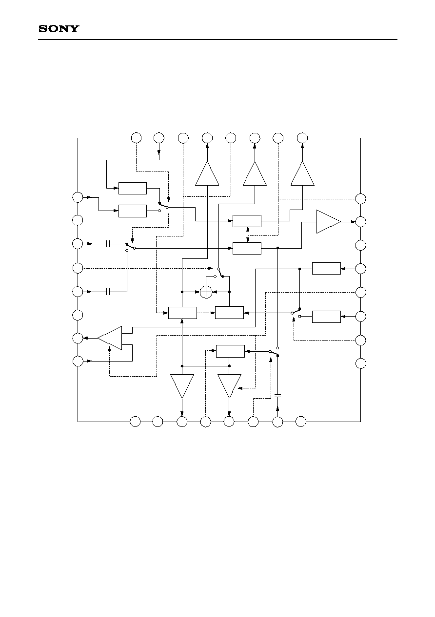
Block Diagram and Pin Configuration
23
24
1
2
3
4
5
6
7
8
9
10
11
12
13
14
15
16
17
18
19
20
21
22
25
30
31
32
26
27
28
29
B
U
F
F
B
U
F
F
BUFF
6
d
B
1
2
d
B
DDS1
MUTE1
MUTE2
MUTE3
CLAMP
CLAMP
CLAMP
CLAMP
DDS2
DRIV
D
R
I
V
YIN2
GND
CIN1
CIN2
Y/VSEL
YOUTGND
YOUT
YINVIN
VOB
COUT1
V
CC
YIN
P.SAVE
EVFYIN
SEL1
YOUTV
CC
I
N
S
E
L
Y
I
N
1
V
O
B
1
E
V
F
C
O
U
T
V
O
W
1
E
V
F
Y
/
V
O
U
T
V
O
W
Y
O
U
T
1
C
O
U
T
G
N
D
V
R
E
G
C
O
U
T
2
C
M
U
T
E
C
O
U
T
S
E
L
2
C
I
N
C
O
U
T
V
C
C

--3--
CXA1812Q
Pin Description
Externally applied voltage
Pin
Symbol
Pin
Equivalent circuit
Description
No.
voltage
1
2
3
4
5
6
COUTGND
VREG
COUT2
CMUTE
COUT
SEL2
0 V
4 V
2.2 V
0 V
2.2 V
0 V
3
60µ
150µ
120µ
GND
2
0
0
V
CC
20µ
7
2
k
150
GND
V
CC
4
GND
V
CC
660µ
660µ
16k
1.2m
2.2V
5
.
3
k
5
GND
V
CC
20µ
150
7
2
k
6
Chroma 75
driver GND.
4 V internal regular output.
Connect a decoupling capacitor.
Do not use for external bias.
Chroma signal output used for
generating a composite video signal.
Control input used for muting both the
chroma signals that are input to Pins 27
(CIN1) and 29 (CIN2) and pass through
the EE path, as well as the chroma
signal that is input from Pin 7 (CIN).
Low (0 to 0.8 V) : normal operation
High (2 V to V
CC
) : mute
Chroma 75
driver output.
Control input used for switching
between the signals input to Pins 27
and 29 and the signal input to Pin 7.
Low (0 to 0.8 V) :
signal at Pin 7 is selected
High (2 V to V
CC
) :
signals at Pins 27 and 29 are selected
314mVp-p
143mVp-p
1.256Vp-p
572mVp-p
--
--

Externally applied voltage
--4--
CXA1812Q
Pin
Symbol
Pin
Equivalent circuit
Description
No.
voltage
7
8
9
10
11
12
CIN
COUTV
CC
YOUTV
CC
SEL1
EVFYIN
P. SAVE
--
4.75 V
4.75 V
0 V
2.5 V
(Sync tip)
0 V
5
0
k
80µ
150 20p
2.2V
7
GND
V
CC
1µ
50µ
2
0
0
1100
GND
V
CC
11
72k
15k
20µ
150
GND
V
CC
12
Video output chroma signal input.
Coupled by means of a capacitor within
the IC.
Inputting a signal of ≠0.3 V or less may
lead waveform distortion.
Chroma 75
driver power supply.
Y 75
driver power supply.
Control input used for switching the
signals that are input from Pins 11
(EVFYIN) and 13 (YIN).
Low (0 to 0.8 V) :
signal at Pin 13 is selected
High (2 V to V
CC
) :
signal at Pin 11 is selected
Y signal input for viewfinder.
Coupled by means of a capacitor ; in
order to keep clamp error to a
minimum, keep the input impedance as
low as possible.
Control input for power saver. When in
power saving mode, the Y and C 75
drivers stop operating. The output of
Pin 31 (YOUT) and Pin 5 (COUT) goes
to high impedance.
Low (0 to 0.8 V) : normal operation
High (2 V to V
CC
) : power saving mode
314mVp-p
143mVp-p
0.5Vp-p
2.5V
--
--
Same as for Pin 6.

Externally applied voltage
--5--
CXA1812Q
Pin
Symbol
Pin
Equivalent circuit
Description
No.
voltage
13
14
15
16
17
18
YIN
V
CC
COUT1
VOB
YOUT1
VOW
2.5 V
(Sync tip)
4.75 V
2.2 V
0 V
1.8 V
(Sync tip)
0 V
7
2
k
20µ
150
GND
V
CC
16
90µ
180µ
2
0
0
GND
V
CC
250µ
17
Video output Y signal input.
Coupled by means of a capacitor; in
order to keep clamp error to a
minimum, keep the input impedance as
low as possible.
Power supply other than the 75
driver.
Video input chroma signal output.
Control input for black level insertion of
the Y signals input to Pins 23 (YIN1)
and 25 (YIN2). The chroma signals
input from Pins 27 and 29 are also
muted simultaneously.
Low (0 to 0.8 V) : normal operation
High (2 V to V
CC
) : insertion mode
Video input Y signal output.
Control input for white level insertion of
the Y signals input to Pins 23 and 25.
The chroma signals input from Pins 27
and 29 are also muted simultaneously.
This pin takes precedence over the Pin
16 control signal.
Low (0 to 0.8V) : normal operation
High (2 V to Vcc) : insertion mode
0.5Vp-p
2.5V
314mVp-p
143mVp-p
0.5Vp-p
1.8V
--
Same as for Pin 3.
Same as for Pin 4.
Same as for Pin 11.

--6--
CXA1812Q
Externally applied voltage
Pin
Symbol
Pin
Equivalent circuit
Description
No.
voltage
19
20
21
22
EVFY/VOUT
VOW1
EVFCOUT
VOB1
1.8 V
(Sync tip)
0 V
2.2 V
0 V
19
180µ
360µ 800µ
16k
GND
V
CC
2.1V
5
.
3
k
21
2
0
0
GND
V
CC
2.2V
20k
2
0
k
200µ
100µ
300µ
Y and composite video signal output for
the viewfinder. A composite video
signal is output when Pin 28 (Y/VSEL)
is high.
Control input for white level insertion of
the Y and composite video signals for
the viewfinder (output from Pin 19).
The chroma signal for the viewfinder
output from Pin 21 (EVFCOUT) is also
muted simultaneously. This pin takes
precedence over the Pin 22 (VOB1)
control signal.
Low (0 to 0.8 V) : normal operation
High (2 V to V
CC
) : insertion mode
Chroma signal output for the
viewfinder. When Pin 28 is high, the
output amplifier goes into power saving
mode and Pin 21 goes to high
impedance.
Control input for black level insertion of
the Y and composite video signals for
the viewfinder. The chroma signal for
the viewfinder is also muted.
Low (0 to 0.8 V) : normal operation
High (2 V to V
CC
) : insertion mode
1.8V
1Vp-p
628mVp-p
286mVp-p
Same as for Pin 4.
Same as for Pin 6.

--7--
CXA1812Q
Externally applied voltage
Pin
Symbol
Pin
Equivalent circuit
Description
No.
voltage
23
25
24
26
27
29
28
30
YIN1
YIN2
INSEL
GND
CIN1
CIN2
Y/VSEL
YOUTGND
2.5 V
(Sync tip)
0 V
0 V
--
0 V
0 V
1100
GND
V
CC
2
0
0
1µ
40µ
23
25
7
2
k
150
GND
V
CC
20µ
20µ
24
Video input Y signal inputs. Coupled
by means of a capacitor; in order to
keep clamp error to a minimum, keep
the input impedance as low as
possible.
Control input for switching between
signals input from Pins 23 and 25 and
from Pins 27 and 29.
Low (0 to 0.8 V) :
signals at Pins 23 and 27 are selected
High (2 V to V
CC
) :
signals at Pins 25 and 29 are selected
GND other than the 75
driver.
Video input chroma signal inputs.
Coupled by means of a capacitor within
the IC.
Inputting a signal of ≠0.3 V or less may
lead waveform distortion.
Control input for switching the output
signal format for Pin 19.
Pin 19 output
Pin 21 output
Low : Y signal
Chroma signal
High : Composite
High impedance
video signal
Low (0 to 0.8 V)
High (2 V to V
CC
)
Y 75
driver GND.
0.5Vp-p
2.5V
314mVp-p
143mVp-p
Same as for Pin 7.
--
--
Same as for Pin 6.

--8--
CXA1812Q
Externally applied voltage
Pin
Symbol
Pin
Equivalent circuit
Description
No.
voltage
31
32
YOUT
YINVIN
1.3 V
(Sync tip)
1.3 V
(Sync tip)
800µ
GND
V
CC
1.2m 1.5m
2
.
7
k
1.2V
8k
31
32
Y 75
driver output.
Y 75
driver feedback input.
2Vp-p
1.3V
0.5Vp-p
1.3V
--9--
CXA1812Q
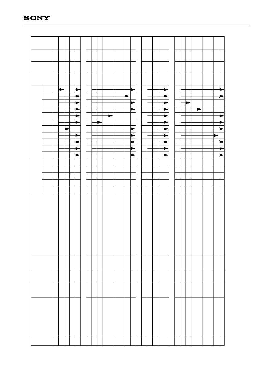
Item
Bias voltage adjustment
Current consumption 1
Current consumption 2
Current consumption PS
VREG voltage
Gain
Frequency response
Secondary distortion
VOB1 level
VOW1 level
DDS1 cross talk
Input SW cross talk
Gain
Frequency response
Secondary distortion
Output D range
Gain
Frequency response
Secondary distortion
VOB2 level
VOW2 level
DDS2 cross talk
Input SW cross talk
Symbol
VADJ
ICC1
ICC2
ICCPS
VREG
G17
F17
HD17
VOB1
VOW1
CT
D1
17
CT
IN
17
G31
F31
HD31
V31
G19
F19
HD19
VOB2
VOW2
CT
D2
19
CT
SE
19
Input
pins
--
--
--
--
--
23, 25
23, 25
23, 25
23, 25
23, 25
23, 25
23, 25
13
13
13
13
11, 13
11, 13
11, 13
11, 13
11, 13
11, 13
11, 13
Measu
rement
point
VADJ
ICC
ICC
ICC
2
17
17
17
17
17
17
17
31A
31A
31A
31A
19
19
19
19
19
19
19
SW conditions
(O
ON)
SW
SW
SW
SW
SW
2
11
13
23
25
O
O
O
O
O
O
O
O
O
O
O
O
O
O
O
O
O
O
O
O
O
O
O
O
Bias conditions (Unit : V)
V
CC
E4
E6
E10
E12
E16
E18
E20
E22
E24
E28
4.75
0.8
0.8
0.8
0.8
0.8
0.8
0.8
0.8
0.8
0.8
2.0
2.0
0.8
0.8
4.75
0.8
0.8
0.8
0.8
0.8
0.8
0.8
0.8
1
0.8
2.0
0.8
2.0
2
2
0.8
0.8
3
4.75
0.8
0.8
0.8
0.8
0.8
0.8
0.8
0.8
0.8
0.8
4.75
0.8
0.8
4
0.8
0.8
0.8
0.8
0.8
0.8
5
2.0
2.0
0.8
6
6
7
0.8
0.8
Measurement conditions
Adjust VADJ pin to 2.85 V with RV
No signal
No signal
No signal
No signal
357 mVp-p, 300 kHz G (300 k)
357 mVp-p, 5 MHz G (5 M)/G (300 k)
357 mVp-p, 5 MHz V (10 M)/V (5 M)
500 mVp-p (Y100 %),
difference between input and Sync tip
500 mVp-p (Y100 %),
difference between input and Sync tip
357 mVp-p, 5 MHz G (CT)/G (5 M)
357 mVp-p, 5 MHz G (CT)/G (5 M)
357 mVp-p, 300 kHz G (300 k)
357 mVp-p, 5 MHz G (5 M)/G (300 k)
357 mVp-p, 5 MHz V (10 M)/V (5 M)
Output amplitude for 679 mVp-p
(Y150 %) input
357 mVp-p, 300 kHz G (300 k)
357 mVp-p, 5 MHz G (5 M)/G (300 k)
357 mVp-p, 5 MHz V (10 M)/V (5 M)
500 mVp-p (Y100 %),
difference between input and Sync tip
500 mVp-p (Y100 %),
difference between input and Sync tip
357 mVp-p, 5 MHz G (CT)/G (5 M)
357 mVp-p, 5 MHz G (CT)/G ( 5M)
Min.
Typ.
Max.
Unit
--
--
--
--
16.0
25.0
35.0
mA
15.0
24.0
34.0
mA
9.5
16.0
22.5
mA
3.90
4.05
4.20
V
≠0.5
0
0.5
dB
≠0.5
0
0.5
dB
≠54
dB
160
180
200
mV
390
410
430
mV
≠74
dB
≠53
dB
5.5
6.0
6.5
dB
≠0.75
≠0.25
0.25
dB
≠54
dB
1.20
1.34
Vp-p
5.5
6.0
6.5
dB
≠0.5
0
0.5
dB
≠51
dB
320
360
400
mV
780
820
860
mV
≠57
dB
≠53
dB
Electrical Characteristics
(Ta=25
∞
C, V
CC
=4.75 V, refer to the electrical characteristics measurement circuit.)
No.
0
1
2
3
4
5
6
7
8
9
10
11
12
13
14
15
16
17
18
19
20
21
22
Y input
Y output
EVF Y output

--10--
CXA1812Q
Item
Gain
Frequency response 1
Frequency response 2
Frequency response 3
Secondary distortion
MUTE level
MUTE cross talk
Input SW cross talk
Gain
Frequency response 1
Frequency response 2
Frequency response 3
Secondary distortion
MUTE level
MUTE cross talk
Input SW cross talk
SEL2 SW cross talk
Gain
Frequency response 1
Frequency response 2
Frequency response 3
Secondary distortion
MUTE level
MUTE cross talk
Input SW cross talk
SEL2 SW cross talk
Symbol
G15A
F
1
15A
F
2
15A
F
3
15A
HD15A
M15A
CT
M
15A
CT
IN
15A
G5A
F
1
5A
F
2
5A
F
3
5A
HD5A
M5A
CT
M
5A
CT
IN
5A
CT
SE
5A
G3A
F
1
3A
F
2
3A
F
3
3A
HD3A
M3A
CT
M
3A
CT
IN
3A
CT
SE
3A
Input
pins
27, 29
27, 29
27, 29
27, 29
27, 29
27, 29
27, 29
27, 29
27, 29
27, 29
27, 29
27, 29
27, 29
27, 29
27, 29
27, 29
27, 29
27, 29
27, 29
27, 29
27, 29
27, 29
27, 29
27, 29
27, 29
27, 29
Measu
rement
point
15
15
15
15
15
15
15
15
5A
5A
5A
5A
5A
5B
5A
5A
5A
3
3
3
3
3
3
3
3
3
SW conditions
(O
ON)
SW
SW
SW
SW
SW
2
11
13
23
25
Bias conditions (Unit : V)
V
CC
E4
E6
E10
E12
E16
E18
E20
E22
E24
E28
4.75
0.8
0.8
0.8
0.8
0.8
0.8
0.8
0.8
8
0.8
2
2
0.8
0.8
9
4.75
0.8
2.0
0.8
0.8
0.8
0.8
0.8
0.8
8
0.8
10
10
10
0.8
0.8
0.8
9
0.8
8
4.75
0.8
2.0
0.8
0.8
0.8
0.8
0.8
0.8
8
0.8
10
10
10
0.8
0.8
0.8
9
0.8
8
Measurement conditions
314 mVp-p, 3.58 MHz G (3.58 M)
314 mVp-p, 2.5 MHz G (2.5 M)/G (3.58 M)
314 mVp-p, 4.43 MHz G (4.43 M)/G (3.58 M)
314 mVp-p, 5.5 MHz G (5.5 M)/G (3.58 M)
314 mVp-p, 4.43 MHz V (8.86 M)/V (4.43 M)
DC differential when mute is off
314 mVp-p, 4.43 MHz G (CT)/G (4.43 M)
314 mVp-p, 4.43 MHz G (CT)/G (4.43 M)
314 mVp-p, 3.58 MHz G (3.58 M)
314 mVp-p, 2.5 MHz G (2.5 M)/G (3.58 M)
314 mVp-p, 4.43 MHz G (4.43 M)/G (3.58 M)
314 mVp-p, 5.5 MHz G (5.5 M)/G (3.58 M)
314 mVp-p, 4.43 MHz V(8.86 M)/V (4.43 M)
DC differential when mute is off
314 mVp-p, 4.43 MHz G (CT)/G (4.43 M)
314 mVp-p, 4.43 MHz G (CT)/G (4.43 M)
314 mVp-p, 4.43 MHz G(CT)/G (4.43 M)
314 mVp-p, 3.58 MHz G (3.58 M)
314 mVp-p, 2.5 MHz G (2.5 M)/G (3.58 M)
314 mVp-p, 4.43 MHz G (4.43 M)/G (3.58 M)
314 mVp-p, 5.5 MHz G (5.5 M)/G (3.58 M)
314 mVp-p, 4.43 MHz V(8.86 M)/V (4.43M)
DC differential when mute is off
314 mVp-p, 4.43 MHz G (CT)/G (4.43 M)
314 mVp-p, 4.43 MHz G (CT)/G (4.43 M)
314 mVp-p, 4.43 MHz G (CT)/G (4.43 M)
Min.
Typ.
Max.
Unit
≠0.8
≠0.3
0.2
dB
≠0.5
0
0.5
dB
≠0.5
0
0.5
dB
≠0.5
0
0.5
dB
≠55
dB
≠15
0
15
mV
≠57
dB
≠66
dB
5.2
5.7
6.2
dB
≠0.5
0
0.5
dB
≠0.5
0
0.5
dB
≠0.5
0
0.5
dB
≠60
dB
≠60
0
60
mV
≠57
dB
≠66
dB
≠78
dB
≠0.8
≠0.3
0.2
dB
≠0.5
0
0.5
dB
≠0.5
0
0.5
dB
≠0.5
0
0.5
dB
≠53
dB
≠15
0
15
mV
≠57
dB
≠70
dB
≠60
dB
No.
23
24
25
26
27
28
29
30
31
32
33
34
35
36
37
38
39
40
41
42
43
44
45
46
47
48
C input 1
C EE 1
C EE 2

--11--
CXA1812Q
Item
Gain
Frequency response 1
Frequency response 2
Frequency response 3
Secondary distortion
MUTE level
MUTE cross talk
Input SW cross talk
SEL2 SW cross talk
Gain
Frequency response 1
Frequency response 2
Frequency response 3
Secondary distortion
MUTE level
MUTE cross talk
Input SW cross talk
SEL2 SW cross talk
Y/V SW cross talk
Gain
Frequency response 1
Frequency response 2
Frequency response 3
Secondary distortion
MUTE level
MUTE cross talk
SEL2 SW cross talk
Symbol
G21A
F
1
21A
F
2
21A
F
3
21A
HD21A
M21A
CT
M
21A
CT
IN
21A
CT
SE
21A
G19A
F
1
19A
F
2
19A
F
3
19A
HD19A
M19A
CT
M
19A
CT
IN
19A
CT
SE
19A
CT
YV
19A
G5B
F
1
5B
F
2
5B
F
3
5B
HD5B
M5B
CT
M
5B
CT
SE
5B
Input
pins
27, 29
27, 29
27, 29
27, 29
27, 29
27, 29
27, 29
27, 29
27, 29
27, 29
27, 29
27, 29
27, 29
27, 29
27, 29
27, 29
27, 29
27, 29
27, 29
7
7
7
7
7
7
7
7
Measu
rement
point
21
21
21
21
21
21
21
21
21
19
19
19
19
19
19
19
19
19
19
5A
5A
5A
5A
5A
5B
5A
5A
SW conditions
(O
ON)
SW
SW
SW
SW
SW
2
11
13
23
25
Bias conditions (Unit : V)
V
CC
E4
E6
E10
E12
E16
E18
E20
E22
E24
E28
4.75
0.8
2.0
0.8
0.8
0.8
0.8
0.8
0.8
8
0.8
11
11
11
11
11
0.8
0.8
0.8
0.8
0.8
9
0.8
8
4.75
0.8
2.0
0.8
0.8
0.8
08
0.8
0.8
8
2.0
11
11
11
11
11
0.8
0.8
0.8
0.8
0.8
9
0.8
8
2.0
0.8
4.75
0.8
0.8
0.8
0.8
0.8
0.8
0.8
0.8
0.8
0.8
2.0
0.8
2.0
Measurement conditions
314 mVp-p, 3.58 MHz G (3.58 M)
314 mVp-p, 2.5 MHz G (2.5 M)/G (3.58 M)
314 mVp-p, 4.43 MHz G (4.43 M)/G (3.58 M)
314 mVp-p, 5.5 MHz G (5.5 M)/G (3.58 M)
314 mVp-p, 4.43 MHz V (8.86 M)/V (4.43 M)
DC differential when mute is off
314 mVp-p, 4.43 MHz G (CT)/G (4.43 M)
314 mVp-p, 4.43 MHz G (CT)/G (4.43 M)
314 mVp-p, 4.43 MHz G (CT)/G (4.43 M)
314 mVp-p, 4.43 MHz G (CT)/G (4.43 M)
314 mVp-p, 3.58 MHz G (3.58 M)
314 mVp-p, 2.5 MHz G (2.5 M)/G (3.58 M)
314 mVp-p, 4.43 MHz G (4.43 M)/G (3.58 M)
314 mVp-p, 5.5 MHz G (5.5 M)/G (3.58 M)
314 mVp-p, 4.43 MHz V (8.86 M)/V (4.43 M)
DC differential when mute is off
314 mVp-p, 4.43 MHz G (CT)/G (4.43 M)
314 mVp-p, 4.43 MHz G (CT)/G (4.43 M)
Min.
Typ.
Max.
Unit
5.2
5.7
6.2
dB
≠0.5
0
0.5
dB
≠0.5
0
0.5
dB
≠0.5
0
0.5
dB
≠52
dB
≠30
0
30
mV
≠58
dB
≠67
dB
≠70
dB
5.2
5.7
6.2
dB
≠0.5
0
0.5
dB
≠0.5
0
0.5
dB
≠0.5
0
0.5
dB
≠52
dB
≠30
0
30
mV
≠53
dB
≠56
dB
≠55
dB
≠54
dB
5.2
5.7
6.2
dB
≠0.5
0
0.5
dB
≠0.5
0
0.5
dB
≠0.5
0
0.5
dB
≠53
dB
≠60
0
60
mV
≠72
dB
≠74
dB
No.
49
50
51
52
53
54
55
56
57
58
59
60
61
62
63
64
65
66
67
68
69
70
71
72
73
74
75
C EE EVF 1
C EE V 1
C output 1

--12--
CXA1812Q
Item
Gain
Frequency response 1
Frequency response 2
Frequency response 3
Secondary distortion
MUTE level
MUTE cross talk
SEL2 SW cross talk
Gain
Frequency response 1
Frequency response 2
Frequency response 3
Secondary distortion
MUTE level
MUTE cross talk
SEL2 SW cross talk
Gain
Frequency response 1
Frequency response 2
Frequency response 3
Secondary distortion
MUTE level
MUTE cross talk
SEL2 SW cross talk
Y/V SW cross talk
Symbol
G3B
F
1
3B
F
2
3B
F
3
3B
HD3B
M3B
CT
M
3B
CT
SE
3B
G21B
F
1
21B
F
2
21B
F
3
21B
HD21B
M21B
CT
M
21B
CT
SE
21B
G19B
F
1
19B
F
2
19B
F
3
19B
HD19B
M19B
CT
M
19B
CT
SE
19B
CT
YV
19B
Input
pins
7
7
7
7
7
7
7
7
7
7
7
7
7
7
7
7
7
7
7
7
7
7
7
7
7
Measu
rement
point
3
3
3
3
3
3
3
3
21
21
21
21
21
21
21
21
19
19
19
19
19
19
19
19
19
SW conditions
(O
ON)
SW
SW
SW
SW
SW
2
11
13
23
25
Bias conditions (Unit : V)
V
CC
E4
E6
E10
E12
E16
E18
E20
E22
E24
E28
4.75
0.8
0.8
0.8
0.8
0.8
0.8
0.8
0.8
0.8
0.8
2.0
0.8
2.0
4.75
0.8
0.8
0.8
0.8
0.8
0.8
0.8
0.8
0.8
0.8
12
12
12
0.8
2.0
0.8
0.8
4.75
0.8
0.8
0.8
0.8
0.8
0.8
0.8
0.8
0.8
2.0
12
12
12
0.8
2.0
0.8
0.8
0.8
0.8
Measurement conditions
314 mVp-p, 3.58 MHz G (3.58 M)
314 mVp-p, 2.5 MHz G (2.5 M)/G (3.58 M)
314 mVp-p, 4.43 MHz G (4.43 M)/G (3.58 M)
314 mVp-p, 5.5 MHz G (5.5 M)/G (3.58 M)
314 mVp-p, 4.43 MHz V (8.86 M)/V (4.43 M)
DC differential when mute is off
314 mVp-p, 4.43 MHz G (CT)/G (4.43 M)
314 mVp-p, 4.43 MHz G (CT)/G (4.43 M)
314 mVp-p, 4.43 MHz G (CT)/G (4.43 M)
Min.
Typ.
Max.
Unit
≠0.8
≠0.3
0.2
dB
≠0.5
0
0.5
dB
≠0.5
0
0.5
dB
≠0.5
0
0.5
dB
≠53
dB
≠15
0
15
mV
≠69
dB
≠77
dB
5.2
5.7
6.2
dB
≠0.5
0
0.5
dB
≠0.5
0
0.5
dB
≠0.5
0
0.5
dB
≠50
dB
≠30
0
30
mV
≠55
dB
≠60
dB
5.2
5.7
6.2
dB
≠0.5
0
0.5
dB
≠0.5
0
0.5
dB
≠0.5
0
0.5
dB
≠54
dB
≠30
0
30
mV
≠63
dB
≠67
dB
≠57
dB
No.
76
77
78
79
80
81
82
83
84
85
86
87
88
89
90
91
92
93
94
95
96
97
98
99
100
C output 2
C EVF output 1
C EVF output 2

--13--
CXA1812Q
Item
Y input
C input
Symbol
CT
YC
3Y
CT
YC
5Y
CT
YC
15Y
CT
YC
21Y
CT
YC
17C
CT
YC
19C
CT
YC
31C
Input
pins
11, 13
23, 25
11, 13
23, 25
11, 13
23, 25
11, 13
23, 25
7, 27
29
7, 27
29
7, 27
29
Measu
rement
point
3
5A
15
21
17
19
31A
SW conditions
(O
ON)
SW
SW
SW
SW
SW
2
11
13
23
25
O
O
O
O
O
O
O
O
O
O
O
O
O
O
O
O
Bias conditions (Unit : V)
V
CC
E4
E6
E10
E12
E16
E18
E20
E22
E24
E28
4.75
0.8
2.0
13
0.8
0.8
0.8
0.8
0.8
14
0.8
0.8
2.0
15
0.8
Measurement conditions
357 mVp-p, 5 MHz G (CT)/G (4.43 M)
357 mVp-p, 5 MHz G (CT)/G (4.43 M)
357 mVp-p, 5 MHz G (CT)/G (4.43 M)
357 mVp-p, 5 MHz G (CT)/G (4.43 M)
314 mVp-p, 4.43 MHz G (CT)/G (4.43 M)
314 mVp-p, 4.43 MHz G (CT)/G (4.43 M)
314 mVp-p, 4.43 MHz G (CT)/G (4.43 M)
Min.
Typ.
Max.
Unit
≠55
dB
≠54
dB
≠55
dB
≠51
dB
≠60
dB
≠45
dB
≠58
dB
No.
101
102
103
104
105
106
107
Cross talk between Y and C (These measurement items are performed with the reference inputs.)
1.
0.8 V for Pin 23 input; 2.0 V for Pin 25 input
2.
With E16 and E18=0.8 V or 2.0 V, measure in all combination modes except for E16=E18=0.8 V
3.
2.0 V for Pin 23 input; 0.8 V for Pin 25 input
4.
0.8 V for Pin 13 input; 2.0 V for Pin 11 input
5.
0.8 V for Y/C output; 2.0 V for V output
6.
With E20 and E22=0.8 V or 2.0 V, measure in all combination modes except for E20=E22=0.8 V
7.
2.0 V for Pin 13 input; 0.8 V for Pin 11 input
8.
0.8 V for Pin 27 input; 2.0 V for Pin 29 input
9.
2.0 V for Pin 27 input; 0.8 V for Pin 29 input
10.
With E4, E16 and E18=0.8 V or 2.0 V, measure in all combination modes except for E4=E16=E18=0.8 V
11.
With E4, E16, E18, E20 and E22=0.8 V or 2.0 V, measure in all combination modes except for E4=E16=E18=E20=E22=0.8 V
12.
With E4, E20 and E22=0.8 V or 2.0 V, measure in all combination modes except for E4=E20=E22=0.8 V
13.
2.0 V for Pin 11 input; 0.8 V for all others
14.
0.8 V for Pins 25 and 29 input; 2.0 V for all others
15.
0.8 V for Pin 7 input; 2.0 V for all others

--14--
CXA1812Q
Electrical Characteristics Measurement Circuit
1
2
3
4
5
6
7
8
9
1
0
1
1
1
2
1
3
1
4
1
5
1
6
1
7
1
8
1
9
2
0
2
1
2
2
2
3
2
4
2
5
2
6
2
7
2
8
2
9
3
0
3
1
3
2
A
T
P
2
T
P
3
T
P
5
B
T
P
5
A
E
4
E
6
7
5
7
5
1
0
µ
1
0
0
µ
S
G
7
7
5
4
7
µ
0
.
0
4
7
µ
C
L
A
M
P
C
L
A
M
P
C
L
A
M
P
C
L
A
M
P
D
D
S
1
D
D
S
2
M
U
T
E
1
M
U
T
E
2
M
U
T
E
3
D
R
I
V
BU
FF
BU
FF
DR
IV
B
U
F
F
6d
B
12
dB
4
V
S
2
R
V
5
0
k
O
P
A
M
P
V
A
D
J
7
5
1
0
k
S
2
5
1
0
µ
T
P
2
5
S
G
2
5
S
G
2
7
S
G
2
9
7
5
7
5
E
2
8
T
P
3
1
B
T
P
3
2
T
P
3
1
A
7
5
1
k
7
5
3
3
0
2
2
0
µ
2
.
2
µ
I
C
C
V
C
C
E
1
6
T
P
1
5
T
P
1
3
0
.
0
4
7
µ
0
.
0
4
7
µ
4
7
µ
4
7
µ
S
1
3
1
0
k
S
1
1
1
0
k
S
G
1
3
S
G
1
1
1
0
µ
T
P
1
1
1
0
µ
E
1
2
7
5
E
1
0
7
5
S
G
2
3
7
5
1
0
k
1
0
µ
T
P
2
1
T
P
2
3
T
P
1
7
T
P
1
9
S
2
3
E
2
4
E
2
2
E
2
0
E
1
8

--15--
CXA1812Q
Application Circuit
1
2
3
4
5
6
7
8
9
1
0
1
1
1
2
1
3
1
4
1
5
1
7
1
8
1
9
2
0
2
1
2
2
2
3
2
4
2
5
2
6
2
7
2
8
2
9
3
0
3
1
3
2
C
L
A
M
P
C
L
A
M
P
C
L
A
M
P
C
L
A
M
P
D
D
S
1
D
D
S
2
M
U
T
E
1
M
U
T
E
2
M
U
T
E
3
D
R
I
V
BU
FF
DR
IV
B
U
F
F
BU
FF
12
dB
6d
B
0
.
0
4
7
µ
0
.
0
4
7
µ
0
.
4
7
µ
4
7
µ
4
7
µ
0
.
0
4
7
µ
V
C
C
(
T
Y
P
:
4
.
7
5
V
)
4
7
µ
0
.
5
V
p
-
p
1
4
3
m
V
p
-
p
3
1
4
m
V
p
-
p
0
.
5
V
p
-
p
1
4
3
m
V
p
-
p
3
1
4
m
V
p
-
p
1
V
p
-
p
0
.
5
V
p
-
p
1
V
p
-
p
o
r
1
V
p
-
p
2
8
6
m
V
p
-
p
6
2
8
m
V
p
-
p
2
8
6
m
V
p
-
p
6
2
8
m
V
p
-
p
1
4
3
m
V
p
-
p
3
1
4
m
V
p
-
p
C
o
n
t
r
o
l
B
l
o
c
k
M
a
i
n
S
i
g
n
a
l
P
r
o
c
e
s
s
i
n
g
B
l
o
c
k
V
i
e
w
f
i
n
d
e
r
S
i
g
n
a
l
P
r
o
c
e
s
s
i
n
g
B
l
o
c
k
C
a
m
e
r
a
S
i
g
n
a
l
P
r
o
c
e
s
s
i
n
g
B
l
o
c
k
0
.
4
7
µ
0
.
4
7
µ
1
0
µ
0
.
0
1
µ
7
5
7
5
7
5
3
9
3
9
7
5
3
9
3
9
7
5
7
5
3
3
0
2
.
2
µ
1
k
2
2
0
µ
1
6
Application circuits shown are typical examples illustrating the operation of the devices. Sony cannot assume responsibility fo
r
any problems arising out of the use of these circuits or for any infringement of third party patent and other right due to same
.

--16--
CXA1812Q
Description of Operation
(Refer to the Pin Description for details on the standard I/O signal levels and the control logic.)
∑ Video Input System
The Y signals input to Pins 23 (YIN1) and 25 (YIN2) are clamped by the respective sync tips, and one of the
signals is selected by the control signal input to Pin 24 (INSEL). Titles are inserted by the control signals input
to Pins 16 (VOB) and 18 (VOW), and after passing through the buffer the signal is output from Pin 17
(YOUT1). Regarding the title insertion levels, the white level is approximately 75IRE and the black level is
approximately 10IRE. Title insertion is described in detail later.
Just as with the Y signals, one of the C signals input to Pins 27 (CIN1) and 29 (CIN2) is selected by the control
signal at Pin 24. The signal is muted to the chroma center level by the control signals at Pins 16 and 18, and
after being branched to EE output, the signal passes through the buffer and is output from Pin 15 (COUT1).
∑ Video Output System
16
18
24
25
23
27
29
15
17
INSEL
VOB
VOW
YIN1
YIN2
CIN1
CIN2
F
r
o
m
e
x
t
e
m
a
l
c
a
m
e
r
a
s
i
g
n
a
l
p
r
o
c
e
s
s
i
n
g
b
l
o
c
k
C input system
Y input system
CLAMP
CLAMP
L
H
L
H
DDS 1
BUFF
BUFF
MUTE 1
YOUT1
COUT1
To video signal
processing block
To C output system (EE)
and VFC output system
YIN
CIN
3
5
4
6
12
7
13
31
32
DRIV
BUFF
DRIV
CLAMP
MUTE 3
From the video
signal processing
block
Y output system
From C input system(EE)
L
H
C output system
To VFY output system
To VFC output system
SEL2
CMUTE
P.SAVE
COUT2
COUT
YOUT
0.01µ
75
220µ
2.2µ
YINVIN
75
1k
330
External
video
output
To composite
video signal
generation circuit

--17--
CXA1812Q
The Y signal input to Pin 13 (YIN) is clamped by the sync tip and is then branched to the Y output system and
the VFY output system. The signal sent to the Y output system passes through the 75
driver (gain=12 dB)
and is then output from Pin 31 (YOUT).
Either the C signal input from Pin 7 (CIN) or the C signal for EE output that was branched from the C input
system is selected by the control signal input to Pin 6 (SEL2). After the signal is muted to the chroma center
level by the control signal input to Pin 4 (CMUTE), the signal is branched to the VFC output system and is also
passed through the 75
driver (gain=12 dB), after which it is output from Pin 5 (COUT). The signal is also
output from Pin 3 (COUT2) for composite video signal generation. The role of Pin 3 is explained in more detail
later.
When Pin 12 (P.SAVE) is set high, it is power saving mode. At this time, the Y and C 75
drivers cease
functioning and the outputs go to high impedance.
∑ VF Video Output System
The Y signals input to Pins 13 and 11 (EVFYIN) are clamped by the respective sync tips, and one of the
signals is selected by the control signal input to Pin 10 (SEL1). When the video signal required for the
viewfinder is different from the signal input to Pin 13, the necessary signal is input from Pin 11. Titles are
inserted by the control signals input to Pins 22 (VOB1) and 20 (VOW1). Just as in the video input system,
regarding the title insertion levels, the white level is approximately 75IRE and the black level is approximately
10IRE. Either this Y signal or the post-Y/C MIX composite video signal is selected by the control signal input
to Pin 28 (Y/VSEL), and then the signal passes through the 12 dB amplifier and is output from Pin 19
(EVFY/VOUT). When Pin 28 is high, the post-Y/C MIX composite video signal is selected. At the same time,
the 6 dB amplifier (for C output) stops functioning in order to reduce the amount of current consumption. At
this time, the output from Pin 21 (EVFCOUT) goes to high impedance.
The C signal for the viewfinder that was branched from the C output system is muted to the chroma center
level by the control signals input to Pins 22 and 20. This signal is input to the Y/C MIX circuit in order to
generate the composite video signal for the viewfinder; the signal is also passed through the 6 dB amplifier and
is output from Pin 21.
EVFYIN
YIN
CMUTE
SEL2
CIN
10
20
22
28
19
21
4
6
7
11
13
EVFY/VOUT
EVFCOUT
To C output system
To Y output system
From C input system (EE)
To VF block
CLAMP
CLAMP
L
H
L
H
DDS 2
MUTE 2
MUTE 3
12dB
6dB
L
H
SEL1
VOB1
VOW1
Y/VSEL

--18--
CXA1812Q
∑ Title Insertion Function (Timing Relationships)
When VOW/VOW1 is high, the Y signal
replaces from the pedestal level to an
electric potential of 75IRE (white character);
when VOB/VOB1 is high, the Y signal
replaces from the pedestal level to an
electric potential of 10IRE (black character).
The C signal replaces to the chroma center
electric potential when VOW/VOW1 or
VOB/VOB1/CMUTE is high.
Because VOW/VOW1 have precedence,
VOW/VOW1 going high results in the
insertion of white character even if
VOB/VOB1 is high. If the settings are as
depicted in the diagram at right, white
character can be bordered with black.
∑ Relationship between Signal Flow and the Title Insertion function, and the Role of Pin 3
Title insertion 2 is performed by a Y/C main
signal processing IC. Although no problem
arises in NTSC system, in the case of PAL
system, because it is necessary to connect a
color spectrum compensation IC with a delay
element between the Y/C main signal
processing IC and the CXA1812Q, if the title
is inserted in the Y/C main signal processing
IC, a temporal deviation occurs in the title
insertion position for Y and C. This problem
is resolved by using MUTE 3 in the C system
only. In addition, because a C signal
processed with MUTE 3 and with no
temporal deviation is output from Pin 3, the
composite video signal can be obtained by
mixing this signal with the Y signal.
<Positioning of the title insertion function within the overall flow of video signal processing>
100 IRE
140 IRE
Bolder
section
Y signal
VOW
VOW1
VOB
VOB1
CMUTE
C signal
10 IRE
75 IRE
Y input
C input
Y output
VF output
C output
CXA1812Q
MUTE 2
DDS 2
MUTE 1
DDS 1
MUTE 3
Title insertion 1
Includes delay element
Color spectrum
compensation IC
(required in PAL
system)
DDS
MUTE
REC
output
PB
input
Title
insertion 2
Pin 3
Composite (V) output
Title insertion 3
Y/C main signal processing IC
Title insertion 1
Title insertion 2
Title insertion 3
REC
output
O
X
X
Y, C, V
output
O
O
X
VF
output
O
O
O
<Relationship between the title insertion position and the inserted signal>

--19--
CXA1812Q
Notes on Operation
∑ Cross talk may become severe, depending on the power supply and the ground connections, and on the
substrate pattern. The power supply and ground connections should be wired so that impedance is as low
as possible, and the signal lines should be located away from other lines.
∑ The power supply pins should be decoupled as closely as possible to the IC. Because Pin 14 (V
CC
) is the
main power supply for this IC, inadequate decoupling can result in a worsening of characteristics such as
distortion and cross talk. Pins 8 (COUTV
CC
) and 9 (YOUTV
CC
) are power supplies for the output stage of
the 75
drivers, and inadequate decoupling can result in oscillation.
∑ If more than the necessary capacitance is connected to the output pins (Pins 3, 5, 15, 17, 19, 21, and 31),
oscillation may result. Wiring should be kept as short as possible.
∑ The frequency response of the Y 75
driver can be controlled by external elements.
The frequency response is raised if capacitance is connected to Pin 32 (YINVIN) versus GND.
The frequency response is attenuated in the high frequency if capacitance is connected between Pin 31
(YOUT) and Pin 32.
∑ When Pin 6 (SEL2) is low, Pin 7 (CIN) and Pin 5 (COUT) have an input/output relationship, so that if more
than the necessary amount of capacitance is connected between these two pins, a loop may be formed and
oscillation may easily result. When designing the board, make sure that there is no parasitic capacitance
between Pins 7 and 5.
∑ Pins 7 (CIN), 27 (CIN1), and 29 (CIN2) are coupled within the IC. If a signal of ≠0.3 V or less is input, a
protective element may cause waveform distortion. When inputting a signal of ≠0.3 V or less, it is
recommended that a suitable DC bias be applied to the input signal.

--20--
CXA1812Q
Ambient temperature vs. Current consumption
35
30
25
20
15
I
C
C
-
C
u
r
r
e
n
t
c
o
n
s
u
m
p
t
i
o
n
(
m
A
)
≠25
0
25
50
75
100
Ambient temperature vs. VREG voltage
V
R
E
G
v
o
l
t
a
g
e
(
V
)
≠25
0
25
50
75
100
Ta-Ambient temperature (∞C)
Ta-Ambient temperature (∞C)
4.080
4.070
4.060
4.050
Frequency response (Y output system)
10
0
≠10
≠20
≠30
G
a
i
n
(
d
B
)
Frequency (Hz)
≠40
≠50
≠60
S
e
c
o
n
d
d
i
s
t
o
r
t
i
o
n
(
d
B
)
100
200
300
400
500
600
Input amplitude (mVp-p)
100k
1M
10M
100M
Vin=357mVp-p
Frequency response (CEE system)
10
0
≠10
≠20
≠30
G
a
i
n
(
d
B
)
Frequency (Hz)
100k
1M
10M
100M
Vin=314mVp-p
Input amplitude vs. Second distortion
(Y output system)
≠40
≠50
≠60
S
e
c
o
n
d
d
i
s
t
o
r
t
i
o
n
(
d
B
)
100
200
300
400
500
600
Input amplitude (mVp-p)
Input amplitude vs. Second distortion
(CEE system)

--21--
CXA1812Q
≠40
≠50
≠60
C
r
o
s
s
t
a
l
k
(
d
B
)
C
r
o
s
s
t
a
l
k
(
d
B
)
C
r
o
s
s
t
a
l
k
(
d
B
)
C
r
o
s
s
t
a
l
k
(
d
B
)
100
200
300
400
500
600
Input amplitude (mVp-p)
Input amplitude vs. Cross talk (EVF output system)
<SEL1 SW cross talk>
≠60
≠70
≠80
100
200
300
400
500
600
Input amplitude (mVp-p)
Frequency vs. Cross talk (EVFY output system)
<SEL1 SW cross talk>
≠30
≠40
≠50
≠60
≠70
S
e
c
o
n
d
a
r
y
d
i
s
t
o
r
t
i
o
n
(
d
B
)
1M
2M
3M
4M
5M
7M
10M
Frequency (Hz)
Input amplitude vs. Cross talk (CEE system)
<SEL2 SW cross talk>
Vin=357mVp-p
Frequency vs. Secondary distortion (Y output system)
≠30
≠40
≠50
≠60
≠70
1M
2M
3M
4M
5M
7M
10M
Frequency (Hz)
Vin=357mVp-p
Frequency vs. Cross talk (CEE system)
<SEL2 SW cross talk>
≠40
≠50
≠60
≠70
≠80
1M
2M
3M
4M
5M
7M
10M
Frequency (Hz)
Vin=314mVp-p
≠30
≠40
≠50
≠60
≠70
S
e
c
o
n
d
a
r
y
d
i
s
t
o
r
t
i
o
n
(
d
B
)
1M
2M
3M
4M
5M
7M
10M
Frequency (Hz)
Vin=314mVp-p
Frequency vs. Secondary distortion (CEE system)

SONY CODE
EIAJ CODE
JEDEC CODE
PACKAGE MATERIAL
LEAD TREATMENT
LEAD MATERIAL
PACKAGE MASS
EPOXY RESIN
SOLDER PLATING
42 ALLOY
32PIN QFP (PLASTIC)
9.0 ± 0.2
7.0 ≠ 0.1 1.5 ≠ 0.15
(
8
.
0
)
0.1 ≠ 0.1
+ 0.2
+ 0.35
+ 0.3
0
.
5
0
0.127 ≠ 0.05
+ 0.1
0∞ to 10∞
0.8 0.3 ≠ 0.1
+ 0.15
1 8
9
32
16
17
24
25
M
0.24
0.2g
QFP-32P-L01
QFP032-P-0707
0.1
Package Outline Unit : mm
CXA1812Q
--22--