 | –≠–ª–µ–∫—Ç—Ä–æ–Ω–Ω—ã–π –∫–æ–º–ø–æ–Ω–µ–Ω—Ç: CXA1842S | –°–∫–∞—á–∞—Ç—å:  PDF PDF  ZIP ZIP |

--1--
E93702-TE
Sony reserves the right to change products and specifications without prior notice. This information does not convey any license by
any implication or otherwise under any patents or other right. Application circuits shown, if any, are typical examples illustrating the
operation of the devices. Sony cannot assume responsibility for any problems arising out of the use of these circuits.
Absolute Maximum Ratings (Ta=25∞C)
∑ Supply voltage
V
CC
14
V
∑ Operating temperature
Topr
≠20 to +75
∞C
∑ Storage temperature
Tstg
≠65 to +150
∞C
∑ Allowable power dissipation
P
D
880
mW
Recommended Operating Conditions
Supply voltage
V
CC
5 to 12
V
Description
The CXA1842S is a bipolar IC which combines 3-
mode surround, bass boosting and vocal
cancellation function into a single chip.
Features
∑ 3-mode surround (surround A, surround B,
simulated stereo)
∑ Vocal cancellation function
∑ Bass boosting function
Applications
CD Radio-cassette tape recorders, equipment with
Karaoke functions
Structure
Bipolar silicon monolithic IC
3-Mode Surround and Vocal Cancellation
22 pin SDIP (Plastic)
CXA1842S
Block Diagram and Pin Configuration
VCA
DET
S6
S4
S5
REF
SW CONT
R1
R2
REF
Vcc
VCA
DET
S6
DET
VCA
S4
≠6
S1
S5
S3
S.S
REF
Rch IN
LPF R1
LPF R2
LPF R3
DET V.C
V.C
B.B
SW1
SW2
REF
Rch OUT
Lch OUT
Vcc
GND
PSN2
PSN1
DET R
DET L
LPF L3
LPF L2
LPF L1
Lch IN
S2
1
2
3
4
5
6
7
8
9
10
11
12
13
14
15
16
17
18
20
21
22
19

--2--
CXA1842S
1
Rch IN
5.0V
22
Lch IN
2
LPF R1
21
LPF L1
3
LPF R2
20
LPF L2
5.0V
4
LPF R3
19
LPF L3
5
DET V.C
17
DET R
0.5V
18
DET L
Channel L
input pin
Channel R
Time constants for L.P.F.
Level detector pin.
To be connected with a
capacitor
V
CC
129
GND
AGND
56K
1
22
32K
80K
AGND
64K
2
3
4
20
21
19
V
CC
129
100K
200
5K
200
500
5
17
18
Pin
Symbol
Pin
Equivalent Circuit
Description
No.
Voltage
Pin Description
(V
CC
=10V, Ta=25∞C)

--3--
CXA1842S
6
V.C
7
B.B
--
8
SW 1
9
SW 2
10
REF
5.0V
11
Rch OUT
5.0V
12
Lch OUT
13
Vcc
10V
14
GND
0
15
PSN 2
5.0V
16
PSN 1
SW is turned ON when this
pin is connected to GND
Reference voltage
(1/2 V
CC
)
Channel R
output pin
Channel L
Power supply
GND pin
The pin to be connected with
a capacitor for time constants
of phase shift
V
CC
129
AGND
V
CC
6
7
8
9
GND
V
CC
48K
48K
AGND
10
129
297
297
V
CC
11
12
V
CC
15
16
Pin
Symbol
Pin
Equivalent Circuit
Description
No.
Voltage
--4--
CXA1842S
C15
10µ
C14
10µ
S7
S2
C12
10µ
S4
S1
C2
10µ
C1
10µ
S5
S6
V
IN
C4
0.1µ
C3
0.1µ
C5
0.022µ
C6
0.022µ
C8
10µ
C7
C9
10µ
S3
10µ
C10
2200p
C11
0.01µ
10V
V1
C13
10µ
R4
10k
10k
R3
Rch IN
LPF R1
LPF R2
LPF R3
DET V.C
V.C
B.B
SW1
SW2
REF
Rch OUT
Lch OUT
Vcc
GND
PSN2
PSN1
DET R
DET L
LPF L3
LPF L2
LPF L1
Lch IN
1
2
3
4
5
6
7
8
9
10
11
12
13
14
15
16
17
18
20
21
22
19
V
Electrical Characteristics
(V
CC
=10V, Ta=25∞C)
O...indicates "ON".
Electrical Characteristics Measurement Circuit
SW conditions
S1 S2 S3 S4 S5 S6 S7
O
O
O
O
O
O
-- -- -- -- -- -- --
O
O
O
O
O
O
O
O
O
O
O
No.
Item
Conditions
Min. Typ. Max. Unit
1 No signal current
Vin=GND
2 Lch gain
Vin=2Vrms, f=1kHz
3 Rch gain
4 Channel balance
Lch gain - Rch gain
5 Lch total harmonic distortion
Vin=2Vrms, f=1kHz
6 Rch total harmonic distortion
7 Lch noise level
Vin=GND
8 Rch noise level
9 Channel separation
Vin=2Vrms, f=1kHz
1.6
3.35
5.1
mA
- 3
0
3
dB
- 3
0
3
dB
- 3
0
3
dB
--
0.07
0.1
%
--
0.07
0.1
%
--
- 90
- 80 dBm
--
- 90
- 80 dBm
55
63
--
dB

--5--
CXA1842S
Mode Switch Correspondence
--...don't care
Bass boosting ON when SW4=ON (Invalid during vocal cancellation)
V
TH
for SW ... V
TH (H)
= V
CC
to 3 V, V
TH (L)
= 2 V to GND
C15
10µ
C14
10µ
SW2
C12
10µ
SW4
SW1
C2
10µ
C1
10µ
C4
0.1µ
C3
0.1µ
C5
0.022µ
C6
0.022µ
C8
10µ
C7
C9
10µ
SW3
10µ
C10
2200p
C11
0.01µ
C13
10µ
Lch OUT
Rch OUT
GND
CXA1842S
GND
Vcc
Lch IN
Rch IN
GND
1
2
3
4
5
6
7
8
9
10
11
12
13
14
15
16
17
18
20
21
22
19
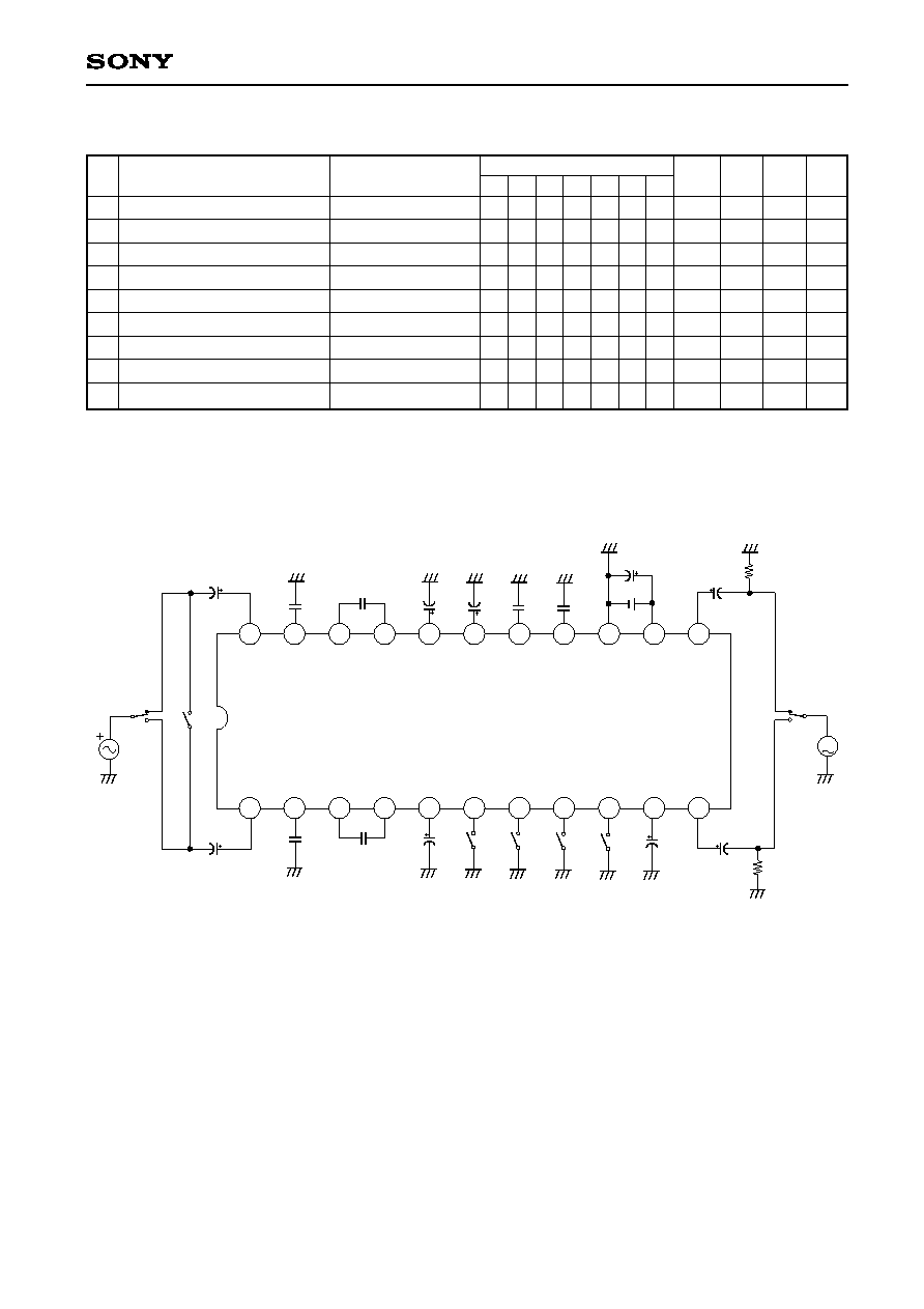
Application Circuit
No.
MODE
SW1
SW2
SW3
1
Simulated Stereo
ON
ON
ON
2
Surround A
ON
OFF
ON
3
Surround B
OFF
ON
ON
4
Pass
OFF
OFF
ON
5
Vocal cancel
--
--
OFF
Application circuits shown are typical examples illustrating the operation of the devices. Sony cannot assume responsibility for
any problems arising out of the use of these circuits or for any infringement of third party patent and other right due to same.

--6--
CXA1842S
Description of Functions
(1) Simulated Stereo
The sum of the L and R signals is input to the Simulated Stereo* (hereafter S.S) block, and a simulated
stereo signal is generated.
(2) Surround A (matrix surround)
The difference of the L and R signals is raised in level by the VCA (maximum 18 dB (typ.)), and is added
to the raw signal.
(3) Surround B
The difference of the L and R signals is raised in level by the VCA (maximum 18 dB (typ.)), is input to the
S.S block, and is then added to the raw signal.
(4) Pass
The L and R signals are output without modification.
(5) Vocal Cancellation
The difference of the L and R signals is input to the S.S block after first passing through the AGC circuit,
and is then output to L and R. In contrast with conventional products, the vocal cancel signal (L-R signal)
is raised in level by the VCA (max. 12 dB typ.), and low frequency part is enhanced, to prevent reduction in
the acoustic pressure level when vocal cancellation is ON.
* Simulated Stereo circuit:
Phases in the audio band are divided into two separate orthogonal channels and treated as L+R and L-R
signals, and are added and subtracted to produce simulated L and R signals. All-pass network.

--7--
CXA1842S
+20
+10
0
≠10
≠20
Surround (dB)
100
1K
10K
Frequency (Hz)
Surround Frequency response
20
10
0
100
1K
10K
Bass boosting production (dB)
Frequency (Hz)
Bass boosting Frequency response
Vin=≠20 dBm
4
3
2
1
5
6
7
8
9
10
11
12
Current consumption (mA)
Supply voltage (V
CC
)
Supply voltage vs. Current consumption
10
0
≠10
≠20
≠30
≠40
≠60
≠50
≠40
≠30
≠20
≠10
0
10
1
2
Output level (dBm)
THD (%)
Input level (dBm)
Input/Output Characteristic
Surround f=50Hz
Sur A f=1kHz
Sur A
BB ON
20
0
≠20
≠40
10
100
1K
10K
Vocal cancellation
Frequency (Hz)
Vocal cancellation Frequency response
Vin=≠40 dBm
Vin=≠10 dBm
Sur B
Lin Rout
Vin=≠50 dBm
Vin=≠30 dBm
Sur B
Rin Rout
Sste Rout
Sste Lout
SONY CODE
EIAJ CODE
JEDEC CODE
PACKAGE STRUCTURE
MOLDING COMPOUND
LEAD TREATMENT
LEAD MATERIAL
PACKAGE WEIGHT
EPOXY RESIN
SOLDER PLATING
COPPER ALLOY
22PIN SDIP (PLASTIC)
SDIP-22P-01
SDIP022-P-0300
0.95g
1.778
11
12
1
22
19.2 ≠ 0.1
+ 0.4
7.62
6.4 ≠ 0.1
+ 0.3
0.25 ≠ 0.05
+ 0.1
0∞ to 15∞
0.5 ± 0.1
0.9 ≠ 0.1
+ 0.15
3.25 ≠ 0.2
+ 0.15
0.51 MIN
3.9 ≠ 0.1
+ 0.4
Package Outline Unit : mm
CXA1842S
--8--