 | –≠–Ľ–Ķ–ļ—ā—Ä–ĺ–Ĺ–Ĺ—č–Ļ –ļ–ĺ–ľ–Ņ–ĺ–Ĺ–Ķ–Ĺ—ā: CXA1843Q | –°–ļ–į—á–į—ā—Ć:  PDF PDF  ZIP ZIP |

High-Speed Sample-and-Hold IC
Description
The CXA1843Q is a bipolar IC designed to sample-
and-hold video and various other signals with high
speed. It is ideal for video and other signal
conversions.
Features
∑ Maximum operating rate = 33MHz (min.)
∑ Low power consumption: 320mW
∑ S/H clock pulse generator circuit
∑ Built-in clock pulse generator for A/D converter
Applications
When used in combination of the CXA1844Q, the
CXA1843Q achieves A/D conversion.
Absolute Maximum Ratings (Ta = 25įC)
∑ Supply voltage V
CC
7
V
V
EE
≠7
V
∑ Input voltage
(VIN pin)
V
IN
V
EE
to AV
CC
+ 0.3
V
(REFIN pin)
V
REFIN
+1 to AV
CC
+ 0.3
V
(CLKIN pin)
V
CLK
GND ≠ 0.5 to DV
CC
+ 0.3 V
(REX 2, 3, 4 pins) V
REX2, 3, 4
GND to GND + 4
V
∑ Reference voltage
(REFFB pin)
V
REFFB
V
EE
to +3
V
(REFOUT pin)
V
REFOUT
V
EE
to AV
CC
+ 0.3
V
∑ Output current
(REFFOUT pin) I
REFOUT
≠1 to +1
mA
(SHOUT pin)
I
SHOUT
≠12 to +12
mA
(CLKOUT pin)
I
ADC
≠1.5 to +1.5
mA
∑ Storage temperature
Tstg
≠65 to +150
įC
∑ Allowable power dissipation
P
D
1.1
W
Operating Conditions
∑ Supply voltage
V
CC
4.75 to 5.25
V
V
EE
≠4.75 to ≠5.25
V
∑ Operating temperature
T
opr
≠20 to +75
įC
Structure
Bipolar silicon monolithic IC
Block Diagram and Pin Configuration
≠ 1 ≠
E92855B7Y
Sony reserves the right to change products and specifications without prior notice. This information does not convey any license by
any implication or otherwise under any patents or other right. Application circuits shown, if any, are typical examples illustrating the
operation of the devices. Sony cannot assume responsibility for any problems arising out of the use of these circuits.
CXA1843Q
32 pin QFP (PIastic)
A/D CONVERTER
PULSE
GENERATOR
SAMPLE HOLD
PULSE
GENERATOR
REF DC
SHIFT
NC
REFFB
REFOUT
AV
EE
3
AV
CC
3
SHOUT
AV
EE
2
NC
NC
DV
EE
1
REX3
REX4
DV
EE
2
DV
CC
3
CLK IN
NC
AV
CC
1
HGND
VIN
AV
EE
1
CGND
NC
NC
NC
DV
CC
2
DV
CC
1
CLKOUT
GND
NC
REX2
REF IN
AV
CC
4
2
3
4
5
6
7
8
9
10
11
12
13
14
15
16
17
18
19
20
21
22
23
24
25
26
27
28
29
30
31
32
1
SAMPLE
HOLD
For the availability of this product, please contact the sales office.

≠ 2 ≠
CXA1843Q
Pin Description
Pin
No.
Symbol
AV
CC1
HGND
VIN
AV
EE1
5V (Typ.)
0V
--
≠5V (Typ.)
CGND
0V
NC
NC
NC
NC
AV
EE2
--
--
--
--
≠5V (Typ.)
SHOUT
Pin voltage
Equivalent circuit
Description
1
2
3
4
5
6
7
8
9
10
11
Analog positive power supply.
Internal resistance GND for
sample-and-hold.
Sample-and-hold-input.
Analog negative power supply.
Internal capacitance GND for
sample-and-hold.
Connect to AGND.
Connect to AGND.
Connect to AGND.
Connect to AGND.
Analog negative power supply.
Sample-and-hold output.
DV
EE2
VIN
130
30k
HGND
AV
CC1
AV
CC1
DV
EE2
CGND
500Ķ
500Ķ
AV
EE1
AV
CC3
DV
EE2
SHOUT

≠ 3 ≠
CXA1843Q
Pin
No.
Symbol
AV
CC3
AV
EE3
REFOUT
REFFB
NC
AV
CC4
REFIN
REX2
NC
5V (Typ.)
≠5V (Typ.)
≠2.8V
As shown in the
Application
Circuit, PNP TR.
is connected
and 2.5V is
applied to
Pin18.
Pin voltage
Equivalent circuit
Description
12
13
14
15
16
17
18
19
20
Analog positive power supply.
Analog negative power supply.
Connect the base of the
external PNP transistor to
create a ≠2V power supply.
Connect the emitter of the
external PNP transistor to
create a ≠2V power supply.
Connect to AGND.
Analog positive power supply.
External DC input for adjusting
the ≠2V power supply.
Connect external resistor that
determines the time interval (T
2
)
between master clock (MCLK)
rise and A/D converter clock
(A/D CLK) fall.
(Normally connect to 1.6k
)
Connect to AGND.
≠2V
As shown in the
Application
Circuit, PNP TR.
is connected
and 2.5V is
applied to
Pin18.
--
5V (Typ.)
2.5V (Typ.)
Approx. 0.5V
When external
resistor is
connected
between Pin 19
and AGND
--
AV
EE3
AV
CC4
130
400Ķ
REFFB
REFOUT
DV
EE2
DV
EE2
GND
REFIN
AV
CC4
130
300Ķ
DV
CC2
REX2
GND
DV
EE2
1k
130
0.5V

≠ 4 ≠
CXA1843Q
Pin
No.
Symbol
GND
CLKOUT
DV
CC1
DV
CC2
NC
DV
EE1
REX3
REX4
DV
EE2
DV
CC3
CLKIN
NC
0V
H:
DV
CC2
≠ 0.78V
L:
DV
CC2
≠ 1.52V
(Typ.)
Approx. 0.5V
When external
resistor is
connected
between Pin 27
and DGND
Pin voltage
Equivalent circuit
Description
21
22
23
24
25
26
27
28
29
30
31
32
GND
A/D converter clock (A/D CLK)
output.
Digital positive power supply.
Digital positive power supply.
Connect to DGND
Digital negative power supply.
Connect external resistor that
determines the time interval (T
3
)
between master clock (MCLK)
rise and sample-and-hold
internal clock (S/H CLK) rise.
(Normally connect 2.7k
)
Connect external resistor that
determines the time interval (T
4
)
between master clock (MCLK)
rise and sample-and-hold
internal clock (S/H CLK) rise.
(Normally connect 1.5k
)
Digital negative power supply.
Digital positive power supply.
Master clock (MCLK) input.
TTL level.
(Vth = 1.5V)
Connect to DGND.
5V (Typ.)
5V (Typ.)
--
≠5V (Typ.)
Approx. 0.5V
When external
resistor is
connected
between Pin 28
and DGND
≠5V (Typ.)
5V (Typ.)
--
--
DV
EE2
GND
DV
CC2
600
2.2mA
CLKOUT
DV
EE2
GND
REX4
REX3
130
130
1k
0.5V
1k
DV
CC2
300Ķ
130
DV
EE2
GND
CLKIN
DV
CC3

≠ 5 ≠
CXA1843Q
Electrical Characteristics
(Ta = 25įC, V
CC
= 5V, V
EE
= ≠5V)
F
IN
= 1kHz, distortion factor
≠55dB
20Log (V
O
(16.5MHz)/V
O
(200kHz)),
Sampling time = 14ns
C
L
= 50pF
V
REFIN
= 2.5V
V
REFIN
= 2.5V
V
CLKIN
= 0V
V
CLKIN
= 5V
V
IN
= ≠1V
V
IN
= ≠2V to 0V
F
IN
= 16.5MHz (2Vp-p)
V
IN
= ≠1V, F
CLK
= 33MHz
F
IN
= 1kHz (2Vp-p),
F
CLK
= 33MHz
Maximun operating rate
F
C
I
CC
I
EE
I
VIN
V
IN
HMDR
HMTH
V
OFFSET
Gsh
Fsh
SR
I
REFIN
V
REFFB
I
CLKL
I
CLKH
V
CLKL
V
CLKH
T
PWH
T
PWL
V
ADCL
V
ADCH
Current consumption
S/H Amplifier Block
V
IN
input current
V
IN
input voltage range
Droop
Feed through
S/H output offset voltage
S/H output gain
S/H output frequency
response
S/H output slew rate
Reference Amplifier Block
REFIN input current
REFFB output voltage
Digital I/O Block
CLKIN input current
CLKIN input voltage
CLKIN clock width
A/D clock low level
A/D clock high level
Item
Symbol
Conditions
Min.
Unit
33
MHz
32
41
50
mA
≠28
≠23
≠18
mA
1
20
50
ĶA
≠2.2
0.2
V
≠20
20
80
mV/Ķs
≠40
≠50
≠70
dB
55
90
120
mV
≠0.5
0.3
0.5
dB
≠1
0.2
1
dB
140
160
200
V/Ķs
0
1
10
ĶA
≠2.2
≠2.0
≠1.8
V
≠10
≠6
0
ĶA
0
0
1
ĶA
0.8
V
2.0
V
9
ns
9
ns
V
CC
≠ 1.52 V
CC
≠ 1.40
V
V
CC
≠ 0.90 V
CC
≠ 0.78
V
Typ.
Max.

≠ 6 ≠
CXA1843Q
Timing Chart
MCLK(Pin 31)
(TTL)
V
IN
(Pin 3)
(0 to ≠2V)
S/H CLK
(Not output to outside)
S/H OUT (Pin 11)
(0 to ≠2V)
A/D CLK (Pin 22)
(PECL)
A/D output (CXA1844Q)
(TTL)
MCLK
(Clock pulse for the
device next to the ADC
in order to latch the
A/D output)
N
N + 1
N + 2
Tsd
T
PWL
T
PWH
T
3
T
4
Hold
taqr
tdr
N ≠ 1
tdf
taqf
2Vp-p
90%
10%
T
1
=
6ns
T
2
t
D
(min)
t
D
(max)
DN ≠ 3
T
S
Th
Threshold
voltage =
1.5V
Threshold
voltage =
V
CC
≠ 1.2V
Threshold
voltage =
1.5V
Threshold
voltage =
1.5V
Threshold
voltage
DN ≠ 2
DN ≠ 1
DN
10%
90%
N + 2
N + 1
N
Hold
Sample
Hold
Sample
Hold
Tsd
Tsd
Sample
MCLK:
System master clock.
S/H CLK:
This clock actuates the internal sample-and-hold circuit.
The internal clock pulse circuit generates the S/H CLK, which is not output outside the IC.
A/D CLK:
This clock actuates the A/D converter. The internal clock buffer circuit generates the A/D CLK.
This clock has the level where +5V is shifted from the ECL level.
T
PWH
, T
PWL
:
S/H CLKIN input clock width
Tsd:
S/H sampling delay for the S/H internal clock
T
1
:
Fixed time interval between master clock rise and A/D CLK rise, T
1
= 6ns (typ.)
T
2
:
Time interval between MCLK rise and A/D CLK fall
T
3
:
Time interval between MCLK rise and S/H CLK rise
T
4
:
Time interval between MCLK rise and S/H CLK fall
t
aqf,
t
df:
10%/90% falling output delay of S/H from MCLK rise
t
aqr,
t
dr:
10%/90% rising output delay of S/H from MCLK rise
t
D
(min., max.): Minimum/maximum output delay of A/D converter (Refer to the CXA1844Q specification.)
Ts:
Setup time of A/D output and MCLK
Th:
Hold time of A/D output and MCLK

≠ 7 ≠
CXA1843Q
(NC)
DV
EE
1
REX3
REX4
DV
EE
2
DV
CC
3
CLKIN
(NC)
(NC)
(NC)
VINL
VINH
(NC)
AGND
(NC)
AV
EE
DV
CC
2
UNDER
OVER
DGND1
AV
CC
1
HGND
VIN
AV
EE
1
CGND
(NC)
(NC)
(NC)
(NC)
REFFB
REFOUT
AV
EE
3
AV
CC
3
SHOUT
AV
EE
2
(NC)
DV
CC
2
DV
CC
1
CLKOUT
GND
(NC)
REX2
REFIN
AV
CC
4
DGND
≠5V
REX3 0.1Ķ DGND
REX4 0.1Ķ DGND
DGND
DGND
≠5V
0.1Ķ
DGND
5V
0.1Ķ
DGND
0.1Ķ
DGND
DGND
MCLK
AGND
0.1Ķ
5V
VIN
≠5V
AGND
AGND
0.1Ķ
AGND
AGND
AGND
AGND
0.1Ķ
AGND
≠5V
AGND
5V
0.1Ķ
0.1Ķ
AGND
AGND
0.1Ķ
AGND
47Ķ
≠5V
AGND
P1
25A1005
AGND
0.1Ķ
47Ķ
5V
0.1Ķ
5V
0.1Ķ
AGND
1k
2k
430
62
REX2
DGND
DGND
DGND
DGND
5V
5V
0.1Ķ
0.1Ķ
DGND
DGND
CXA1843Q
50
200
D1
5V
50
0.1Ķ
AGND
AGND
≠5V
5V
0.1Ķ
AGND
0.1Ķ
DGND
DGND
DGND
DGND
DGND
DGND
DGND
5V
0.1Ķ
≠5V
DGND
DGND
0.1Ķ
PS
ENABLE
MINV
LINV
DGND
0.1Ķ
AGND
DGND
AGND
AGND
AGND
0.1Ķ
0.1Ķ
0.1Ķ
AGND
AGND
47Ķ
PS
ENABLE
CLK
MINV
LINV
(NC)
DGND2
DV
EE
DGND1
DV
CC
1
DGND1
DGND1
(NC)
V
REFBS
V
REFB
V
REF3
V
REF2
V
REF1
V
REFT
V
REFTS
(NC)
(NC)
DGND3
DGND4
DGND1
DGND1
UNDER
OVER
D0
D1
D2
D3
D4
D5
D6
D7
D8
D9
D0
D1
D2
D3
D4
D5
D6
D7
D8
D9
CXA1844Q
TTL
VIN = 2Vp-p (max) DC ≠ 1V
2
3
4
5
6
7
8
9
10
11
12
13
14
15
16
17
18
19
20
21
22
23
24
25
26
27
28
29
30
40
39
38
37
36
35
34
31
32
33
41
42
43
44
45
46
47
48
1
2
3
4
5
6
7
8
9
10
11
12
13
14
15
16
17
18
19
20
21
22
23
24
25
26
27
28
29
30
31
32
1
Application Circuit
Application circuits shown are typical examples illustrating the operation of the devices. Sony cannot assume responsibility for
any problems arising out of the use of these circuits or for any infringement of third party patent and other right due to same.
Symbol
REX2
REX3
REX4
External resistance
1.6k
2.7k
1.5k
Metal film resistors must be connected
to the REX2 to REX4 pins.
CXA1843Q External Resistance

≠ 8 ≠
CXA1843Q
Notes on Operation
(1) In circuit board layout, it is necessary that the AGND and DGND patterns be as large as possible and that
double or more layer pattern be used to make low impedance.
(2) To prevent digital system noise interference with the analog system, the AGND and DGND, AV
CC
and
DV
CC
, AV
EE
and DV
EE
on the PCB must be separated from each other. However, connect the AV
EE
and
DV
EE
with coil and others to prevent the generation of differential voltage.
(3) The AV
CC
, DV
CC
, AV
EE
and DV
EE
pins must be connected to the AGND or DGND respectively via ceramic
chip capacitors those are 0.1ĶF or more, as close to the pin as possible.
(4) The length of the wiring between the S/H SHOUT and A/D converter V
IN
should be as short as possible.
(5) The range of the signal input to V
IN
(Pin 3) of the sample-and-hold circuit is 0 to ≠2V.
(6) Adjust the V
REFIN
applied voltage so that V
REFFB
= f ≠ 2V.
(7) As shown in the Block Diagram, the amplifier input and output are internally connected to the REFOUT
and REFFB pins. To generate REFFB voltage for the reference voltage of A/D converter, the connection
of an external PNP transistor (hFE
100 (typ.)) is required as shown in the Application Circuit.
(8) Make the S/H DV
CC2
voltage equal to the A/D converter DV
CC1
voltage.

≠ 9 ≠
CXA1843Q
Example of Representative Characteristics
42
41
40
39
75
50
25
0
≠25
Ta [įC]
I
CC
[mA]
I
CC
vs. Ta
≠21
≠22
≠23
≠24
75
50
25
0
≠25
Ta [įC]
I
EE
[mA]
I
EE
vs. Ta
43
42
38
36
5.25
5
4.75
V
CC
[V]
I
CC
[mA]
I
CC
vs. V
CC
41
40
39
37
≠19
≠20
≠24
≠25
≠4.75
≠5
≠5.25
V
EE
[V]
I
EE
[mA]
I
EE
vs. V
EE
≠21
≠22
≠23
100
85
80
5.25
5
4.75
V
CC
[V]
V
OFFSET
[mA]
V
OFFSET
vs. V
CC
95
90
100
85
80
≠4.75
≠5
≠5.25
V
EE
[V]
V
OFFSET
[mA]
V
OFFSET
vs. V
EE
95
90
VIN = ≠2V
VIN = ≠1V
VIN = 0V
VIN = ≠2V
VIN = ≠1V
VIN = 0V

≠ 10 ≠
CXA1843Q
120
100
80
60
75
50
25
0
≠25
Ta [įC]
V
OFFSET
[mV]
V
OFFSET
vs. Ta
≠1.4
≠1.6
≠2.2
≠2.6
3
2.5
2
V
REFFIN
≠ Input voltage [V]
V
REFFB
≠ A/D converter reference voltage [V]
A/D converter reference voltage vs. Input voltage
≠1.8
≠2
≠2.4
≠1.99
≠1.995
≠2.01
75
25
≠25
Ta [įC]
V
REFFB
≠ A/D converter reference voltage [V]
≠2
≠2.005
≠2.004
≠2.007
≠2.008
≠4.75
≠5
≠5.25
V
EE
[V]
V
REFFB
≠ A/D converter reference voltage [V]
≠2.005
≠2.006
110
90
VIN = ≠2V
VIN = ≠1V
VIN = 0V
70
50
0
≠2.009
≠2.01
≠2.004
≠2.007
≠2.008
5.25
5
4.75
V
CC
[V]
V
REFFB
≠ A/D converter reference voltage [V]
≠2.005
≠2.006
≠2.009
≠2.01
A/D converter reference voltage vs Ta
(V
REFFIN
= 2.5V)
A/D converter reference voltage vs. V
CC
(V
REFFIN
= 2.5V)
A/D converter reference voltage vs. V
EE
(V
REFFIN
= 2.5V)

≠ 11 ≠
CXA1843Q
40
30
20
10
3
2
1
0
T
2
[ns]
T
2
vs. REX2
1
0.5
≠0.5
≠1
75
50
25
0
≠25
Ta [įC]
A/D clock width Tpwh variation [ns]
A/D clock width Tpwh (T
2
-T
1
) variation vs. Ta
(Ta = 25įC typ.)
1
≠0.5
≠1
5.25
5
4.75
V
CC
[V]
0.5
0
35
25
15
REX2 [k
]
For normal use. REX = 21.6k
0
A/D clock width Tpwh (T
2
-T
1
) variation vs. V
CC
(V
CC
= 5.0V typ.)
1
≠0.5
≠1
≠4.75
≠5
≠5.25
V
EE
[V]
0.5
0
A/D clock width Tpwh (T
2
-T
1
) variation vs. V
EE
(V
EE
= ≠5.0V typ.)
45
30
15
5
3
2
tdr, tdf, taqr, taqf [ns]
40
35
S/H output delay (tdr, tdf) vs. REX3
(taqr, taqf) vs. REX4
1.5
≠1
≠1.5
75
25
≠25
Ta [įC]
S/H output delay variation [ns]
0.5
0
S/H output delay variation vs. Ta
(Ta = 25įC typ.)
≠0.5
1
0
50
20
25
4
2.8
2
1.1
For normal use, REX3 = 2.7k
REX4 = 1.5k
REX3 [k
]
REX4 [k
]
taqf
taqr
tdr
tdf
A/D clock width Tpwh variation [ns]
A/D clock width Tpwh variation [ns]

≠ 12 ≠
CXA1843Q
1
≠0.5
≠1
5.25
5
4.75
V
CC
[V]
S/H output delay variation [ns]
0.5
0
S/H output delay variation vs. V
CC
(V
CC
= 5.0V typ.)
1
≠0.5
≠1
≠4.5
≠5
≠5.5
V
EE
[V]
0.5
0
S/H output delay variation vs. V
EE
(V
EE
= ≠5.0V typ.)
0.001
Input frequency [MHz]
S/N ratio [dB]
Input frequency vs. S/N ratio for CXA1843Q + CXA1844Q (clock frequency = 33MHz)
60
55
50
45
40
35
30
0.01
0.1
1
10
20
Amplitude = 2Vp-p
Amplitude = 1Vp-p
S/H output delay variation [ns]

≠ 13 ≠
CXA1843Q
S/H + A/D EVALUATION BOARD
The S/H + A/D Evaluation Board is a printed circuit board for evaluating the 10-bit 33MSPS high speed
sample-and-hold IC (CXA1843Q) and 2-step A/D converter (CXA1844Q). This board is designed to enable
users to make full use of the performance of CXA1843Q + CXA1844Q and evaluate them easily.
Features
∑ Resolution
10bit
∑ Maximum operating conversion speed
33MSPS
∑ 2 types analog input
V
IN
input (OP AMP input) and DIR. IN input (AC coupled input) are available.
∑ Analog input dynamic range
2Vp-p
∑ Digital output level
TTL
∑ Power supply voltage
Ī5V
∑ Built-in D/A converter (For evaluation)
Generates the analog waveform.
Block Diaram
Counter
CLK/8
CLK/16
CLK/4
CLK/2
S2
CLK
Buffer
Buffer
50
DGND
CLK input
(CON4)
Latch
CON
10
10
TTL
ECL
10bit D/A
10
10
CLK/N
AGND
V
EE
FULSCAL ADJ
D/A OUT
(CON3)
V
EE
(≠5V)
GND V
CC
(+5V)
MCLK
OFFSET ADJ
VR1
AGND
Analog input
VIN (CON1)
AGND
AGND
VIN
50
50
Analog input
DIR.IN (CON2)
OP
AMP
◊
2
AGND
2.5V
A
B
S1
REX2
REX3
REX4
1.6k
2.7k
1.5k
10
A/D OUT
A/D CLK
S/H OUT
18
≠
2.0V
VREFBS
SW1
Latch
PS
ENABLE
MINV
LINV
DAINV
S/H + A/D Evaluation Board Block Diagram
VR2
CLK/N
VRBS
VRB
VIN L VIN H
10bit A/D
REF IN REFB
S/H
≠ 14 ≠
CXA1843Q
Connection and Setting for S/H + A/D Evaluation Board
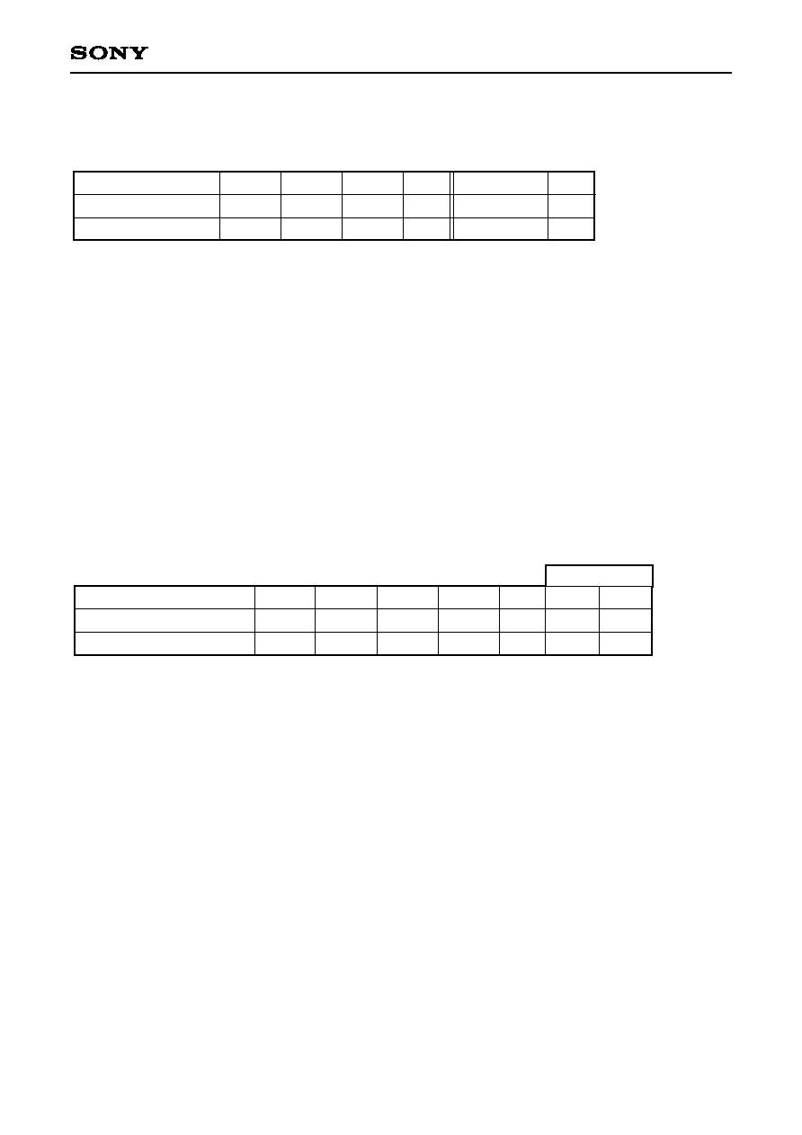
1. Power supply voltage (CON6)
Item
Min.
Typ.
Max.
Unit
Vcc
+4.75
+5.0
+5.25
V
V
EE
≠5.25
≠5.0
≠4.75
Typical current
220
≠400
V
Unit
mA
mA
2. Analog input (CON1, CON2) and offset adjustment (VR1)
[V
IN
Input] (CON1)
When the amplitude of an analog input signal supplied to the sample-and-hold is 1Vp-p and its input range is
within 1.0V to ≠0.9V, the board is able to amplify its amplitude by two times using the operation amplifier. The
S1 selector should be short-circuited at side A and opened at side B, and the analog input is added from
CON1. In this case, offset adjustment is required at the VR1, so that the dynamic range of the analog input
signal can be set to a value between 0V to ≠2V by monitoring the V
IN
pin.
[DIR IN. Input] (CON2)
When the input supplied to the sample-and-hold is a recurring signal (sine wave, etc.) without offset, it is
added using the AC coupled input from CON2 by connecting a 10k
resistor to side A and a 0.1ĶF capacitor
to side B of the S1 selector. In this case, offset adjustment is required at the VR1, so that the dynamic range
of the analog input signal can be set to a value between 0V to ≠2V by monitoring the V
IN
pin.
Item
Min.
Typ.
Max.
DIR. IN input (CON2)
≠2.0
0
2.0
V
IN
input (CON1)
≠0.9
1.0
Amplitude
2.0
1.0
Unit
V
V
A
10k
short
B
0.1ĶF
open
S1 setting
3. Clock input (CON4)
TTL compatible
Use in the 30 to 70% CLK duty range
(CON4 is terminated to DGND at 50
on the board.)
4. Digital output (CON5)
TTL compatible
C-MOS (ACT series) output
(CON1 and CON2 are terminated to AGND at 50
on the board.)

≠ 15 ≠
CXA1843Q
5. D/A out (CON3) and full-scale adjustment (VR2)
The output waveforms of the D/A converter are output from CON3. When an oscilloscope or other such
instrument is used for monitoring, a 50
terminating resistor is required. The full-scale output voltage must
also be adjusted. And the output amplitude should also be adjusted to 1Vp-p by the VR2.
Item
Min.
Typ.
Max.
Unit
D/A OUT
≠1.0
0
V
6. SW1 setting
These are the switches for PS, ENABLE, MINV, and LINV of the A/D converter and the DAINV of the D/A
converter. Normally all are used ON.
7. S2 setting
This is the selection of the frequency division ratio for the clock which is supplied to the D/A converter.
Normally, 1/1 is used but the ratios from 1/2 to 1/16 are also used for the envelope test or other tests.

≠ 16 ≠
CXA1843Q
N
N + 1
N + 2
T4
T3
Sample
S
S
Hold
H
H
N
N + 1
N + 2
T2
T1
Tpwh
Tpwl
tdmax
tdmin
N ≠ 2
N ≠ 1
N
N ≠ 3
N ≠ 2
N ≠ 1
N ≠ 4
N ≠ 3
N ≠ 2
N ≠ 3
N ≠ 2
N ≠ 1
N ≠ 4
N ≠ 3
N ≠ 2
Latch CLK input
(TTL)
Latch Data out
(TTL)
CON5 Data out
(TTL)
DAC Data input
(ECL)
DAC CLK input
(ECL)
DAC Data OUT
(0 to ≠1V)
AD Data out
(TTL)
AD CLK
(PECL)
SH Analog out
(0 to ≠2V)
SH CLK
(internal)
MCLK
(TTL)
CLK input
(TTL)
Analog input
(0 to ≠2V)
TH
TL
CXA1843Q + CXA1844Q PCB Timing Chart
Item
Symbol
Min.
Typ.
Max.
S/H CLK delay
T3
20
A/D CLK delay
A/D CLK width
A/D output data delay
T4
33
Unit
ns
ns
T1
6
T2
20
ns
ns
tpwh
14
tpwl
13
ns
ns
td
4
18
ns

≠ 17 ≠
CXA1843Q
S/H + A/D Evaluation Board Parts List
(No.)
(Product Name)
(Function)
(No.)
(Product Name)
(Function)
IC.1
CXA1843Q
Sample Hold
R1, 13, 38
FRD-25SR (0.25W)
51
IC.2
CXA1844Q
10bit ADC
R21, 25
FRD-25SR (0.25W)
100
IC.3
CLC505
OP-AMP
R2, 22
FRD-25SR (0.25W)
270
IC.4
CX20201A-1
DAC
R3, 4
FRD-25SR (0.25W)
470
IC.5
74ACT34
Buffer R23
FRD-25SR
(0.25W)
1k
IC.6 74ACT163
Counter
R12
FRD-25SR
(0.25W)
4.7k
IC.7
74ACT16821
Latch
R5, 8, 15, 16, 18, 19
FRD-25SR (0.25W)
10k
IC.8, 9
MB767
ECL
TTL level translator
R24
FRD-25SR (0.25W)
51k
D1, 3
TL431CP
3-pin shunt regulator
R11
FRD-25SR (0.25W)
150k
D2
1S1555
Diode
R9
SN14C2F
1.5k
P1 2SA1175
PNP
transistor
R14
SN14C2F
1.6k
SW.1
DSS-105
Switch
R10
SN14C2F
2.7k
CON.1 to 4 TMA5502-10
SMA connector
R6, 7, 17, 20
Chip resistor
CON.5
FAP-2601-1201
Flat cable connector
RN1 to 3
RGLD 4X621J
620
CON.6
TJ-563
Power supply connector
C2, 9 to 17, 19, 23 to 32
Chip capacitor
0.1ĶF
S1.3
JX-1
Short-pin
34 to 40, 42 to 60
VR1.2
RJ-6P
2k
volume resistor
C1, 6 to 8, 33, 41
Tantalum capacitor
1ĶF (Voltage proof of 35V)
C1 to 11
LS-2S
Check pin
C3 to 5, 20 to 22
33ĶF (Voltage proof of 35V)
C18
Ceramic capacitor
100pF
L1 to 4
SF-T5-30-03
30ĶF
Precautions
1. The monitoring pins are designed to be easily grounded in order to minimize distortions occurring when
monitoring waveforms on an oscilloscope. Waveform monitoring is facilitated by using the grounded tip
(part No. 013-1185-00) made by Tektronix at the end of the probe.
2. VR1 and VR2 are optimally adjusted and set before the board is shipped.
3. REX2, REX3, REX4 (R14, R10, R9) on the board use metal-oxide resistor, and T2, T3, T4 are optimally
adjusted and set within the range of 1MHz to 33MHz.

≠ 18 ≠
CXA1843Q
S/H + A/D EVALUATION BOARD (Component Side)
S/H + A/D EVALUATION BOARD (Solder Side)

≠ 19 ≠
CXA1843Q
2Q7
AV
CC
AGND
AGND
D1
C
A
Vref
R2 270
C1 1Ķ
C2
0.1Ķ
AGND
R3 470
R5 10k
VR1 2K
OFFSET
ADJ
AGND
AV
CC
C6 1Ķ
C8 1Ķ
AGND
AGND
C15 0.1Ķ
R8 10k
R4 4.7k
R1 51
AGND
CON.1
VIN
7
1
5
8
2
3
4
6
AGND
C7 1Ķ
AGND
AGND
C14 0.1Ķ
AV
EE
IC.3
C18 100P
R11 150k
A
B
R12 47
AGND
CON.2
DIR.in
9
10
11
12
13
14
15
16
17
18
19
20
21
22
23
24
25
26
27
28
29
30
31
32
2
3
4
5
6
7
8
1
C13
0.1Ķ
DGND
DV
EE
C12 0.1Ķ
R10 2.7k
C9
0.1Ķ
DGND
R9 1.5k
DV
EE
C11 0.1Ķ C10 0.1Ķ
DV
CC
DGND
DV
CC
DGND
R6
R7
AV
CC
C19 0.1Ķ
AV
EE
C23 0.1Ķ
CXA1843Q
C32
0.1Ķ
C31 0.1Ķ
C30 0.1Ķ
C29 0.1Ķ
AV
CC
AV
EE
C28 0.1Ķ
AGND
C16
0.1Ķ
C17 0.1Ķ
DGND
C24 0.1Ķ
R14 1.6k
DGND
AGND
C25 0.1Ķ
C26 0.1Ķ
AV
CC
DV
EE1
REX3
REX4
DV
EE2
DV
CC3
CLK IN
NC
NC
NC
REFFB
REFOUT
AV
EE3
AV
CC3
SHOUT
AV
EE2
NC
DV
CC2
DV
CC1
CLK OUT
GND
NC
REX2
REFIN
AV
CC4
AV
CC1
HGND
VIN
AV
EE1
CGND
NC
NC
NC
100
R21
C39
DV
CC
DGND
13
14
15
16
17
18
19
20
21
22
23
24
25
26
27
28
29
30
36
35
34
31
32
33
40
39
38
37
41
42
43
44
45
46
47
48
AGND
R17
R20
AGND
AV
CC
AV
EE
0 .1Ķ
C38
0 .1Ķ
D2
C44
0 .1Ķ
OVER
UNDER
0.1Ķ
C27
C33 1Ķ
VREFBS
AGND
AGND
C34
0.1Ķ
C35
0.1Ķ
C36
0.1Ķ
AGND
C2
DGND
VREFTS
0 .1Ķ
C40
0 .1Ķ
C45
DV
EE
DV
CC
DGND
DGND
0 .1
Ķ
C37
R18
10k
R15
10k
R19
10k
R16
DVCC
PS
ENABLE
MINV
LINV
DAINV
DGND
SW1
CXA1844Q
PS
ENABLE
CLK
MINV
LINV
NC
DGND2
DV
EE
DGND1
DV
CC1
GND1
GND1
NC
VINL
VINH
AVF
AV
EE
DV
CC2
UNDER
OVER
GND1
NC
NC
NC
NC
DGND4
VREFTS
VRFET
NC
DGND3
VRFEB
VRFE1
VRFE2
VRFE3
VREFBS
NC
D9
GND1
D5
D8
D7
D6
D3
D2
D1
D0
GND1
D4
15
16
17
18
19
20
21
22
23
24
25
26
27
28
0.1Ķ
C47
1Ķ
C41
VR2 2K
C43 0.1Ķ
FULL
SCALE ADJ
1k
R23
AGND
AV
EE
DV
EE
DGND
AGND
0 .1Ķ
C46
C42
0.1Ķ
51k
R24
CON.3
D/A out
AGND
DV
EE
INV
DGND
AGND1
NC
OUT
NC
NC
NC
NC
AV
EE
VREF
AGND2
CLKB
CLK
NC
NC
D10
D9
D8
D7
D6
D5
D4
D3
D2
D1
CX20201A-1
620
R27
620
R28
620
R29
0.1Ķ
C49
DGND
620
R31
620
R32
620
R33
0.1Ķ
C50
DGND
620
R35
620
R36
620
R37
0.1Ķ
C51
DGND
620
R30
RN3
620
R34
100
R25
0 .1
Ķ
C48
DGND
DV
EE
2
3
4
5
6
7
8
9
10
11
12
1
DGND
NC
MCLK
VIN
S/H out
IC.2
IC.1
DV
CC2
DGND2
DGND2
CON.5
CLK
LSB
D1
D3
D4
D5
D6
D7
D8
MSB
D2
DGN
D
DGND2
DV
CC2
0.1Ķ
C60
11
12
13
14
15
16
17
18
19
20
OUT1
IN1
IN2
IN3
IN4
S
V
CC
IN5
IN6
IN7
IN8
OUT2
OUT3
OUT4
V
EE
GND
OUT5
OUT6
OUT7
OUT8
IC.9
MB767
DGND2
C57
0.1Ķ
DV
CC2
DGND2
C58
0.1Ķ
DVEE2
2
3
4
5
6
7
8
9
10
1
OUT1
IN1
IN2
IN3
IN4
S
V
CC
IN5
IN6
IN7
IN8
OUT2
OUT3
OUT4
V
EE
GND
OUT5
OUT6
OUT7
OUT8
IC.8
MB767
DGND2
C52
0.1Ķ
DV
CC2
DGND2
C53
0.1Ķ
DV
EE2
2
3
4
5
6
7
8
9
10
1
29
30
40
39
38
37
36
35
34
31
32
33
41
42
43
44
45
46
47
48
49
50
51
52
53
54
55
56
1OE_
IC.7
2
3
4
5
6
7
8
9
10
11
12
13
14
15
16
17
18
19
20
21
22
23
24
25
26
27
28
1
1Q1
1Q2
GND
1Q3
1Q4
V
CC
1Q5
1Q6
1Q7
GND
1Q8
1Q9
1Q10
2Q1
2Q2
2Q3
GND
2Q4
2Q5
2Q6
V
CC
GND
2Q9
2Q10
2OE_
1CLK
1D1
1D2
GND
1D3
1D4
V
CC
1D5
1D6
1D7
GND
1D8
1D9
1D10
2D1
2D2
2D3
GND
2D4
2D5
2D6
V
CC
2D7
2D8
GND
2D9
2D10
2CLK
DGND2
DGND2
DGND2
0.1Ķ
C59
DGND2
LSB
C1
C2
C3
C4
C5
C6
C7
C8
MSB
DGND2
DGND2
DGND2
DGND2
DGND2
DGND2
0.1Ķ
C59
DGND2
11
12
13
14
15
16
17
18
19
20
CLK
MSB
LSB
D1
D2
D3
D4
D5
D6
D7
D8
8
9
10
11
12
13
14
2
3
4
5
6
7
1
GND
3Y
3A
2Y
2A
1Y
1A
4Y
4A
5Y
5A
6Y
6A
V
CC
74ACT34
IC.5
DV
CC2
DGND2
0.1Ķ
C54
DGND2
15
16
9
10
11
12
13
14
8
2
3
4
5
6
7
1
51
R38
DGND2
DGND2
DV
CC2
DV
CC2
DGND2
0.1Ķ
C56
1/1
1/2
1/4
1/8
1/16
S2
CLK
CLEAR
A IN
B IN
C IN
D IN
EN P
GND
V
CC
RCarry
A OUT
B OUT
C OUT
D OUT
EN T
LOAD
CLK
CON.4
DGND2
74ACT163
IC.6
DV
CC2
620
R26
2
3
4
5
6
7
8
9
10
11
12
13
14
1
D3
C
A
Vref
21
R1
P1
DV
CC
AGND
R13 51
S1
C1
P3
C3
C4
37
48
36
24
25
13
12
1
9
8
1
32
16
17
24
25
P2
P1
1
28
15
14
RN2
RN1
1
56
29
28
11
10
20
1
20
1
11
10
1
14
8
71
6
1
8
9
AGND
DGND
DGND2
7Ķ
H
GND
GND
V
EE
V
CC
DGND2
DV
EE2
(≠5V)
DV
EE2
33Ķ
C5
L2
7Ķ
H
AV
EE
(≠5V)
AV
EE
33Ķ
AGND
C3
DV
EE
(≠5V)
DV
EE
33Ķ
C4
L1
DGND
DGND2
DV
CC2
(+5V)
DV
CC2
33Ķ
C22
L4
7Ķ
H
AV
CC
(+5V)
AV
CC
33Ķ
AGND
C20
DV
CC
(+5V)
DV
CC
33Ķ
C21
L3
DGND
7Ķ
H
CON.6
C6
C8
C10
C11
C9
C7
C5
P4
ADCLK
CLK
DGN
D
DGN
D
DGN
D
DV
CC
D9
D8
D7
D6
D5
D4
D3
D2
D1
D0
ACT1682
1
2Q8
10k
S/H + A/D Evaluation Board

≠ 20 ≠
CXA1843Q
Package Outline
Unit: mm
SONY CODE
EIAJ CODE
JEDEC CODE
PACKAGE MATERIAL
LEAD TREATMENT
LEAD MATERIAL
PACKAGE MASS
EPOXY RESIN
SOLDER PLATING
42 ALLOY
32PIN QFP (PLASTIC)
9.0 Ī 0.2
7.0 ≠ 0.1
1.5 ≠ 0.15
(8.0)
0.1 ≠ 0.1
+ 0.2
+ 0.35
+ 0.3
0.50
0.127 ≠ 0.05
+ 0.1
0į to 10į
0.8
0.3 ≠ 0.1
+ 0.15
1
8
9
32
16
17
24
25
M
0.24
0.2g
QFP-32P-L01
QFP032-P-0707
0.1