 | –≠–Ľ–Ķ–ļ—ā—Ä–ĺ–Ĺ–Ĺ—č–Ļ –ļ–ĺ–ľ–Ņ–ĺ–Ĺ–Ķ–Ĺ—ā: CXA1851N | –°–ļ–į—á–į—ā—Ć:  PDF PDF  ZIP ZIP |
--1--
E93505-TE
Sony reserves the right to change products and specifications without prior notice. This information does not convey any license by
any implication or otherwise under any patents or other right. Application circuits shown, if any, are typical examples illustrating the
operation of the devices. Sony cannot assume responsibility for any problems arising out of the use of these circuits.
Absolute Maximum Ratings
(Ta=25įC)
∑ Supply voltage
Vcc
5
V
∑ Operating temperature
Topr
≠20 to +75
įC
∑ Storage temperature
Tstg
≠65 to +150
įC
∑ Allowable power dissipation
P
D
530
mW
When mounted on a 505
◊
0
◊
1.6 mm copper-
foiled glass epoxy board
Recommended Operating Conditions
Supply voltage
Vcc
2.7 to 4.5
V
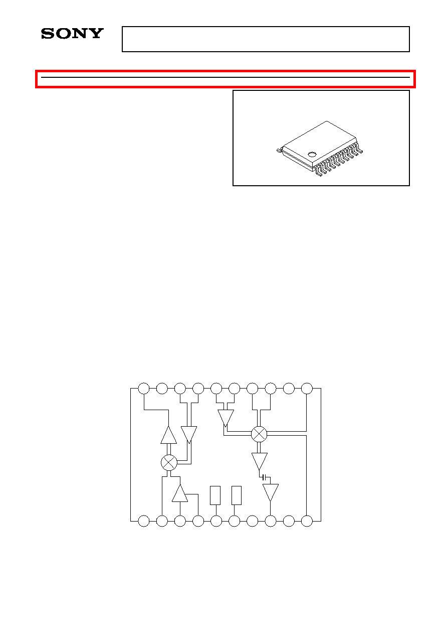
Description
The CXA1851N is an up/down converter IC for
900 MHz-band mobile communications.
This is suitable for 900 MHz-band digital cordless
telephone (CT2) and digital cellular.
Features
∑ Transmission/reception converter on a single chip
∑ Operating frequency: 800 to 900 MHz
∑ Supply voltage: 2.7 to 4.5 V
∑ Power saving function
∑ 20-pin SSOP package used for set size reduction
Applications
∑ CT2 digital cordless telephone
∑ Digital cellular
Structure
Bipolar silicon monolithic IC
Up/Down Converter for 900 MHz-Band Mobile Communications
20 pin SSOP (Plastic)
CXA1851N
RE
G
RE
G
RF
A
M
P
R
F
PR
E AM
P
O
S
C
B
U
FFE
R
AM
P
IF
A
M
P
MIX
MIX
LN
A
GN
D
RF
b
R
F
IN
PEAKI
N
G
OU
T
P/
S (
D
)
P/
S (
U
)
V
cc (
U
)
R
F
OU
T
GN
D
MI
X
O
U
T
1
IF
OU
T
V
cc (
D
)
L
O
IN
(
D
)
LO
b (
D
)
LO
b (
U
)
L
O
IN
(
U
)
IF
IN
IF
b
GN
D
MI
X
O
U
T
2
1
2
3
4
5
6
7
8
9
10
11
12
13
14
15
16
17
18
20
19
Block Diagram and Pin Configuration
For the availability of this product, please contact the sales office.

--2--
CXA1851N
Pin Description
Typical pin
voltage (V)
1
GND
0.0
GND pin for the down converter.
2
RF BYPASS
1.1
MIX input by-pass pin for the down
converter.
3
RF INPUT
0.9
RF input pin for the down
converter. Because of high
impedance, a 4.7 nH external chip
inductor should be used for
impedance matching.
4
PEAKING
0.12
Emitter pin for the low-noise
OUT
amplifier. Connect an approximate-
ly 3 pF chip capacitor and an
approximately 22
chip resistor in
series to the GND.
5
P/S
0 to 4.5
Power saving control pin for the
(for DOWN
down converter.
CONV.)
OFF when Vp/s
1.0 V; ON when
Vp/s
1.8 V
6
P/S
0 to 4.5
Power saving control pin for the up
(for UP
converter.
CONV.)
OFF when Vp/s
1.0 V; ON when
Vp/s
1.8 V
7
V
CC
2.7 to 4.5
Power supply for the up converter.
(for Up
CONV.)
8
RF OUTPUT
2.7
RF output pin for the up converter.
(Vcc=2.7V)
Connect this pin to the Pin 7 power
supply via the 15 nH chip inductor.
9
GND
0.0
GND pin for the up converter RF
amplifier.
REG
REG
2
3
4
5
6
REG
8
Pin No.
Symbol
Equivalent circuit
Description

--3--
CXA1851N
Typical pin
voltage (V)
10
MIX OUT1
2.3
MIX output pin for the up
converter.
11
MIX OUT2
2.3
MIX output pin for the up
converter. Connect an approxi-
mately 4.7 nH chip inductor and
an approximately 3.5 pF chip
capacitor between this pin and
Pin 10 to form a tank circuit.
12
GND
0.0
GND pin for the oscillator buffer
amplifier and mixer blocks of the
up converter.
13
IF BYPASS
1.03
IF input by-pass pin for the up
converter.
14
IF INPUT
1.03
IF input pin for the up converter.
Because of high impedance, an
external matching circuit is
necessary which consists of a 220
nH chip inductor and an
approximately 1.5 pF chip
capacitor.
15
OSC INPUT
1.8
Oscillator input pin for the up
(for UP
converter. A matching circuit
CONV.)
consisting of a 51
resistor is
necessary.
16
OSC
1.8
Oscillator input by-pass pin for the
BYPASS
up converter.
(for UP
CONV.)
17
OSC
1.85
Oscillator input by-pass pin for the
BYPASS
down converter.
(for DOWN
CONV.)
18
OSC
1.85
Oscillator input pin for the down
BYPASS
converter. A matching circuit
(for DOWN
consisting of a 51
resistor is
CONV.)
necessary.
19
Vcc
2.7 to 4.5
Power supply for the down
(for DOWN
converter.
CONV.)
20
IF OUTPUT
1.45
IF output pin for the down
converter.
10
11
REG
13
14
15
16
17
18
20
Pin No.
Symbol
Equivalent circuit
Description

--4--
CXA1851N
Item
Symbol
Conditions
Min.
Typ.
Max.
Unit
Up Converter Block
1
Current consumption
I
CC
For no signal input
18.0
25.0
35.0
mA
Conversion gain
CG
Pin= - 40dBm
17.5
20.5
25.5
dB
RF output power
Pout
Pin= -10dBm, 50
load
0
3
dBm
Noise figure
NF
DSB mode
13
18
dB
Lo leak
ISO (Lo)
Pin= - 10dBm
- 25.0
- 10
dBm
IF leak
ISO (IF)
Pin= - 10dBm
- 12.0
- 5
dBm
Standby current consumption
I
CC
(PD)
6pin (P/S)<1.0V
220
2 350
2
ĶA
Power saving control voltage
Vp/s (ON)
1.8
4.5
V
Vp/s (OFF)
1.0
V
Rise time
Tup
2.5
5.0
Ķs
Down Converter Block
3
Current consumption
I
CC
For no signal input
8.0
15.0
22.0
mA
Conversion gain
CG
Pin= - 40dBm, 50
load
15.0
18.0
23.0
dB
IF output power
Pout (IF)
Pin= - 10dBm, 50
load
- 4.5
- 2.0
dBm
Third-order intermodulation distortion IM3
f
RF
1=866.4MHz, Pin1= - 40dBm
45
49.0
dBc
f
RF
2=866.8MHz, Pin2= - 40dBm
Noise figure
NF
DSB mode
7.5
10
dB
Standby current consumption
I
CC
(PD)
5pin (P/S)
1.0V
220
2 350
2
ĶA
Power saving control voltage
Vp/s (ON)
1.8
4.5
V
Vp/s (OFF)
1.0
V
Rise time
Tup
2.5
5.0
Ķs
Electrical Characteristics
(Ta=25įC, V
CC
=2.7V, Z
L
=Z
S
=50
)
1: f
IF
in=150.05MHz, f
RF
out=864.05 to 868.05MHz
f
L
oin=1014.10 to 1018.1MHz (- 9dBm)
2: These are the total values for the up and down converters.
3: f
RF
in=864.05 to 868.05MHz
f
L
oin=1014.10 to 1018.1MHz (- 9dBm)
Typical Reference characteristics
(Ta=25įC, V
CC
=2.7V, Z
L
=Z
S
=50
)
Item
Symbol
Conditions
Typ.
Unit
Up Converter Block
Third-order intermodulation distortion
IM3
fIF1=150.4MHz, P
IF
1= - 30dBm
39.0
dBc
fIF2=150.8MHz, P
IF
2= - 30dBm
Down Converter Block
1 dB compression
P- 1dB
Output conversion, 50
load
- 7.0
dBm
Lo leak
ISO (Lo)
Pin= - 40dBm
- 29.0
dB
RF leak
ISO (RF)
Pin= - 40dBm
- 44.0
dB

--5--
CXA1851N
RE
G
RE
G
RF
A
M
P
R
F
PR
E AM
P
O
S
C
B
U
FFE
R
AM
P
IF
A
M
P
MIX
MIX
LN
A
GN
D
RF
b
R
F
IN
PEAKI
N
G
O
U
T
P/
S (
D
)
P/
S (
U
)
V
cc (
U
)
R
F
OU
T
GN
D
MI
X
O
U
T
1
IF
OU
T
V
cc (
D
)
L
O
IN
(
D
)
LO
b (
D
)
LO
b (
U
)
L
O
IN
(
U
)
IF
IN
IF
b
GN
D
MI
X
O
U
T
2
15n
120p
4.
7N
3p
22
4.
7N
120p
120p
120p
51
30p
30p
30p
30p
51
120p
120p
1.
5p
IF SG
LO SG
220n
10p
4.7N
1500p
180p 1500p
1
2
3
4
5
6
7
8
9
10
11
12
13
14
15
16
17
18
20
19
Electrical Characteristics Test Circuit 1

--6--
CXA1851N
Electrical Characteristics Test Circuit 2
Items: NF (D), NF (U)
RE
G
RE
G
RF
A
M
P
R
F
PR
E AM
P
O
S
C
B
U
FFE
R
AM
P
IF
A
M
P
MIX
MIX
LN
A
GN
D
RF
b
R
F
IN
PEAKI
N
G
O
U
T
P/
S (
D
)
P/
S (
U
)
V
cc (
U
)
R
F
OU
T
GN
D
MI
X
O
U
T
1
IF
OU
T
V
cc (
D
)
L
O
IN
(
D
)
LO
b (
D
)
LO
b (
U
)
L
O
IN
(
U
)
IF
IN
IF
b
GN
D
MI
X
O
U
T
2
15n
120p
4.
7N
3p
22
4.
7N
120p
120p
120p
51
30p
30p
30p
30p
51
120p
120p
1.
5p
220n
10p
4.7N
NF
M
E
T
E
R
NOISE
SOURCE
NOISE
SOURCE
NF
M
E
T
E
R
LOSG
1500p
180n 1500p
1
2
3
4
5
6
7
8
9
10
11
12
13
14
15
16
17
18
20
19

--7--
CXA1851N
FM DE
M
O
D
◊
5
139.
35M
H
z
27.
87M
H
z
R
SSI
BI
T
ST
R
EAM
R
SSI
F
R
EE C
H
DE
T
E
CT
I
O
N
150.
05M
H
z
PL
L
1014 t
o
1018.
2M
H
z
PL
L
SW
864 t
o
868.
2M
H
z
1 t
o
10m
W
TX GC
A
RX
LN
A
F/
F
300.
1M
H
z
150.
05M
H
z
C
X
A
1852N
(QU
A
D
R
A
T
U
R
E
M
O
D
U
L
A
T
O
R
)
C
X
A
1744R
(I
F
A
M
P)
I
Q
C
X
A
1851N
(U
P/
D
O
W
N
C
O
NV
E
R
TE
R
)
10.
7M
H
z
Block diagram
Digital cordless telephone chip set (CXA1744R/CXA1851N/CXA1852N)

--8--
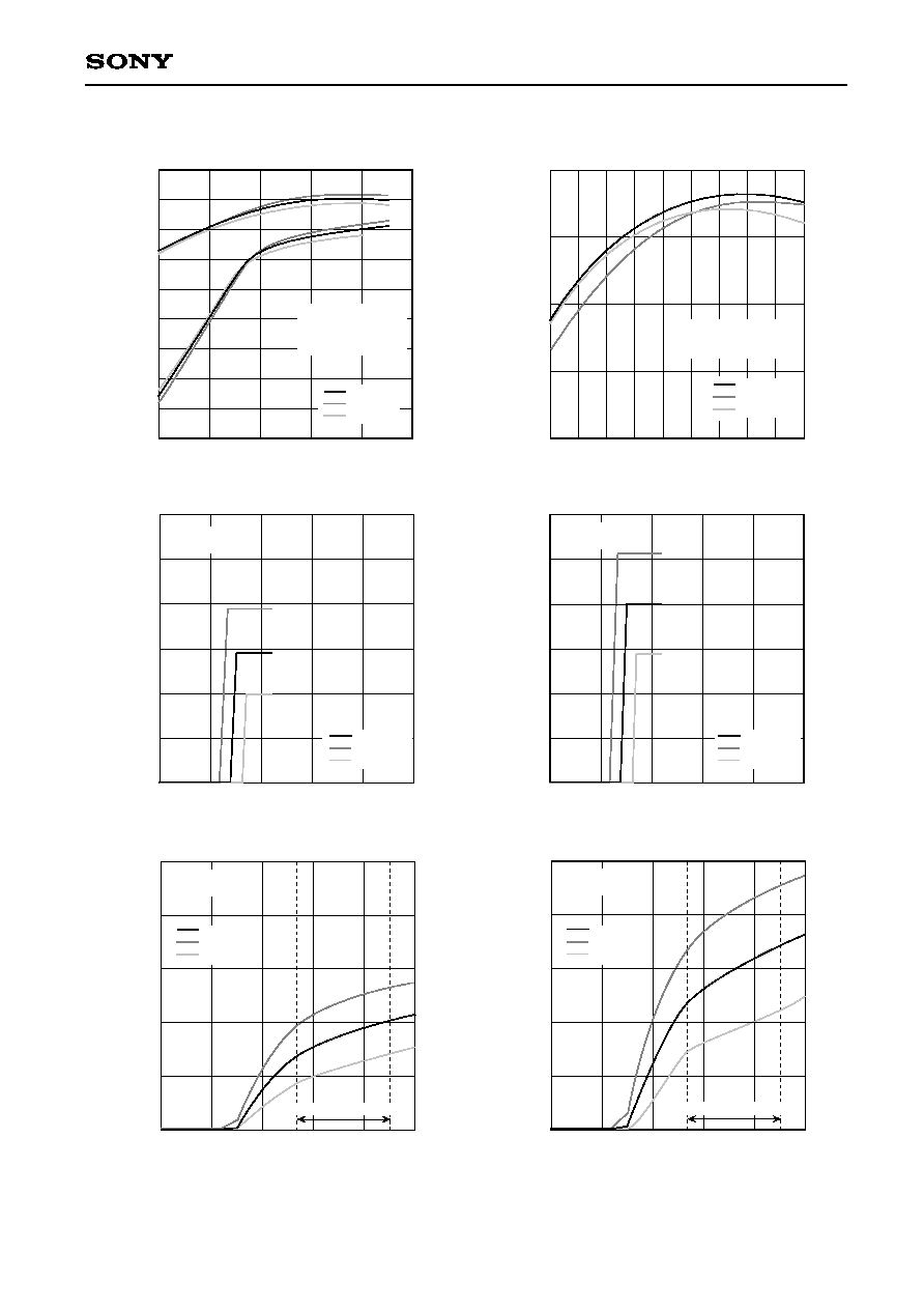
CXA1851N
(Down-Con) f
RF
vs. NF characteristics
5.0
100
500
1000
f
RF
(MHz)
NF (dBm)
Vcc=2.7V
LO sweep (- 9dBm)
(Down-Con) Pin vs. Pout and IM3 characteristics
10
0
Pin (dBm)
Pout, 3rd order distortion (dBm)
0
- 10
- 20
- 30
- 40
- 50
- 60
- 70
- 80
- 40
- 30
- 20
- 10
10
Vcc=2.7V
RF
1
=866.4MHz
RF
2
=866.8MHz
LO=1016Hz (- 9dBm)
DS3 (Down-Con) L
O
input level vs. CG characteristics
0
L
O
Input level (dBm)
CG (dB)
25
20
15
10
5
-27
- 18
- 12
- 6
Vcc=2.7V
RF=866MHz (- 40dBm)
LO=1016Hz (- 9dBm)
- 24
- 15
- 9
- 3
- 21
15.0
10.0
(Down-Con) f
RF
vs. CG characteristics
10.0
100
500
1000
f
RF
(MHz)
CG (dBm)
Vcc=2.7V
LO sweep (- 9dBm)
RF sweep (- 40dBm)
IF=150MHz
20.0
15.0
(Down-Con) f
RF
vs. NF characteristics
5.0
100
500
1000
f
RF
(MHz)
NF (dBm)
Vcc=4.5V
LO sweep (- 9dBm)
15.0
10.0
(Down-Con) f
RF
vs. CG characteristics
10.0
100
500
1000
f
RF
(MHz)
CG (dBm)
25.0
15.0
20.0
Vcc=4.5V
LO sweep (- 9dBm)
RF sweep (- 40dBm)
IF=150MHz
Ta=25įC
Ta=80įC
Ta=-30įC
Ta=25įC
Ta=80įC
Ta=-30įC
Ta=25įC
Ta=80įC
Ta=-30įC
Ta=25įC
Ta=80įC
Ta=-30įC
Ta=25įC
Ta=80įC
Ta=-30įC
Ta=25įC
Ta=80įC
Ta=-30įC
--9--
CXA1851N
(Down-Con) Pin vs. Pout and IM3 characteristics
10
0
Pin (dBm)
Pout, 3rd order distortion (dBm)
0
- 10
- 20
- 30
- 40
- 50
- 60
- 70
- 80
- 40
- 30
- 20
- 10
10
Vcc=4.5V
RF
1
=866.4MHz
RF
2
=866.8MHz
LO=1016Hz (- 9dBm)
(Down-Con) L
O
input level vs. CG characteristics
0
L
O
input level (dBm)
CG (dB)
25
20
15
10
5
-27
- 18
- 12
- 6
Vcc=4.5V
RF=866MHz (- 40dBm)
LO=1016Hz (- 9dBm)
- 24
- 15
- 9
- 3
- 21
(Down-Con) P/S voltage level vs. I
CC
characteristics
30.0
4.0
P/S voltage level (V)
Icc (mA)
15.0
10.0
5.0
0
0
1.0
2.0
3.0
5.0
Vcc=2.7V
No signal input
25.0
20.0
(Down-Con) P/S voltage level vs I
CC
characteristics
30.0
4.0
P/S voltage level (V)
Icc (mA)
15.0
10.0
5.0
0
0
1.0
2.0
3.0
5.0
Vcc=4.5V
No signal input
25.0
20.0
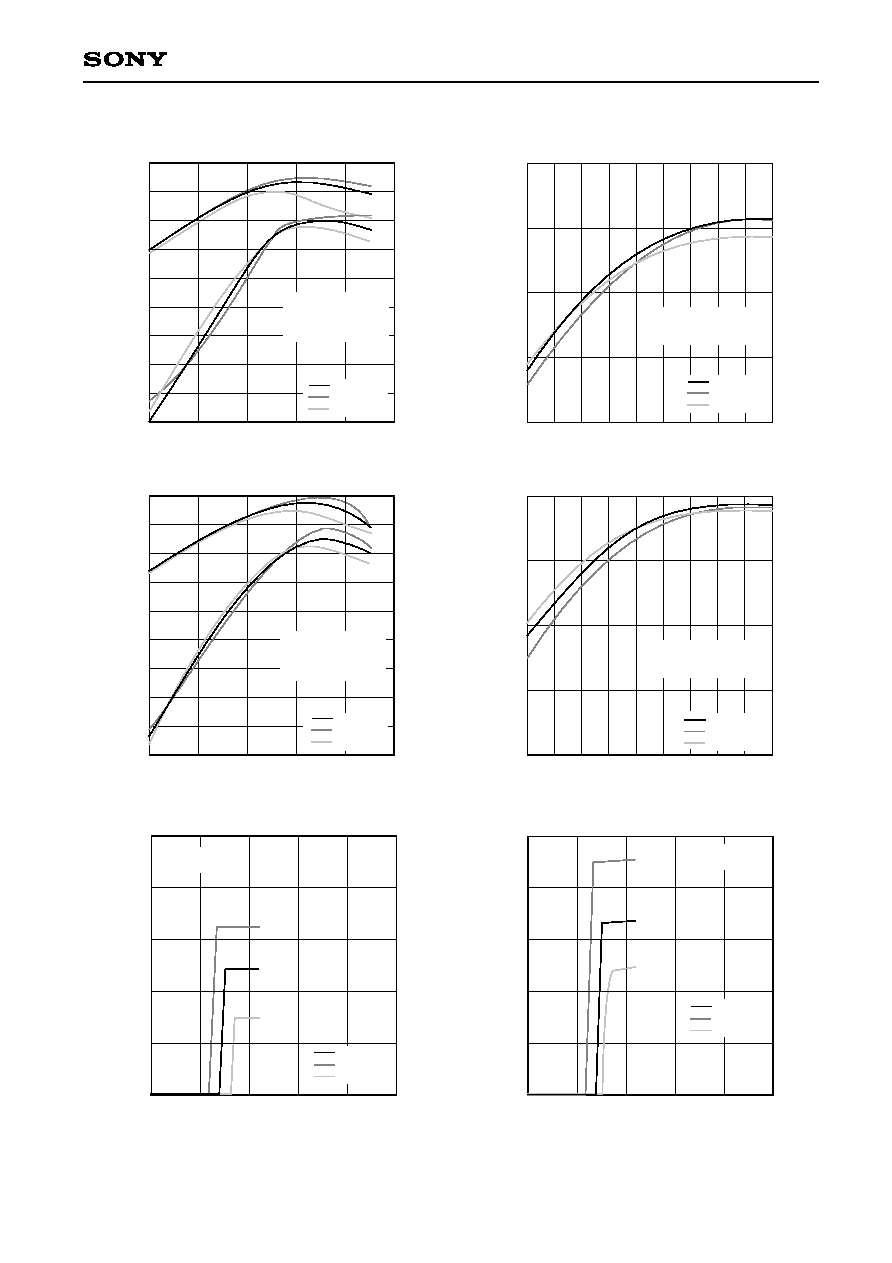
(Up-Con) Vcc vs. I
CC
characteristics
50
4.0
Vcc (V)
Icc (mA)
20
10
0
0
1.0
2.0
3.0
5.0
Vcc=V
P/S
No signal input
40
30
2.7
4.5
Recommended operating range
(Down-Con) Vcc vs. I
CC
characteristics
50
4.0
Vcc (V)
Icc (mA)
20
10
0
0
1.0
2.0
3.0
5.0
Vcc=V
P/S
No signal input
40
30
2.7
4.5
Recommended operating range
Ta=25įC
Ta=80įC
Ta=-30įC
Ta=25įC
Ta=80įC
Ta=-30įC
Ta=25įC
Ta=80įC
Ta=-30įC
Ta=25įC
Ta=80įC
Ta=-30įC
Ta=25įC
Ta=80įC
Ta=-30įC
Ta=25įC
Ta=80įC
Ta=-30įC
--10--
CXA1851N
(Up-Con) Pin vs. Pout and IM3 characteristics
10
0
Pin (dBm)
Pout, 3rd order distortion (dBm)
0
- 10
- 20
- 30
- 40
- 50
- 60
- 70
- 80
- 40
- 30
- 20
- 10
10
Vcc=2.7V
IF
1
=150.4MHz
IF
2
=150.8MHz
LO=1016Hz (- 9dBm)
(Up-Con) L
O
input level vs. CG characteristics
0
L
O
input level (dBm)
CG (dB)
25
20
15
10
5
-27
- 18
- 12
- 6
Vcc=2.7V
IF=150MHz (- 40dBm)
LO=1016Hz
- 24
- 15
- 9
- 3
- 21
(Up-Con) Pin vs. Pout and IM3 characteristics
10
0
Pin (dBm)
Pout, 3rd order distortion (dBm)
0
- 10
- 20
- 30
- 40
- 50
- 60
- 70
- 80
- 40
- 30
- 20
- 10
10
Vcc=4.5V
IF
1
=150.4MHz
IF
2
=150.8MHz
LO=1016Hz (- 9dBm)
(Up-Con) L
O
input level vs. CG characteristics
0
L
O
input level (dBm)
CG (dB)
25
20
15
10
5
-27
- 18
- 12
- 6
Vcc=2.7V
IF=150MHz (- 40dBm)
LO=1016Hz
- 24
- 15
- 9
- 3
- 21
(Up-Con) P/S voltage level vs. I
CC
characteristics
50
4.0
P/S voltage level (V)
Icc (mA)
10
0
0
1.0
2.0
3.0
5.0
Vcc=2.7V
No signal input
30
20
(Down-Con) P/S voltage level vs. I
CC
characteristics
4.0
P/S voltage level (V)
Icc (mA)
0
1.0
2.0
3.0
5.0
Vcc=2.7V
No signal input
40
50
10
0
30
20
40
Ta=25įC
Ta=80įC
Ta=-30įC
Ta=25įC
Ta=80įC
Ta=-30įC
Ta=25įC
Ta=80įC
Ta=-30įC
Ta=25įC
Ta=80įC
Ta=-30įC
Ta=25įC
Ta=80įC
Ta=-30įC
Ta=25įC
Ta=80įC
Ta=-30įC

--11--
CXA1851N
Notes on Operation
(1) Electrostatic sensitive diveces because of the high-frequency process.
(2) Earth pattern should be as wide as possible and do not increase ground impedanse to prevent from the
parasitic osellation.
(3) Wire the GND pin as short as possible.
(4) Connect a by-pass capacitor to the V
CC
pin.

CXA1851N
--12--
SONY CODE
EIAJ CODE
JEDEC CODE
M
PACKAGE STRUCTURE
MOLDING COMPOUND
LEAD TREATMENT
LEAD MATERIAL
PACKAGE WEIGHT
EPOXY / PHENOL RESIN
SOLDER PLATING
20PIN SSOP (PLASTIC)
7.0 MAX
0.65
0.22 ≠ 0.05
+ 0.10
1.0 Ī
0.1
4.4 Ī
0.1
1.5 Ī
0.1
1.8 MAX
0.575 MAX
0.15
0.10
0.15 ≠ 0.05
+ 0.10
A
0.1 Ī 0.1
0į to 10į
0.5 Ī
0.2
DETAIL A
SSOP-20P-L072
SSOP020-P-0225-BN
1
10
11
20
COPPER ALLOY
0.1g
6.4 Ī
0.2
Package Outline
Unit : mm