Description
The CXA1917AM/AS is a bipolar IC designed for
use in the Dolby S type noise reduction system (NR).
An external operational amplifier is required to
configure the decoder. The stereo Dolby B-C-S type
NR combines use of a CXA1563M/S and two
CXA1917AM/AS ICs.
Features
∑ Considerable reduction in the number of external parts
(half compared to CXA1417S/Q)
∑ The same Dolby level as that of CXA1560 series ICs (≠6dBm)
Structure
Bipolar silicon monolithic IC
Absolute Maximum Ratings (Ta = 25∞C)
∑ Supply voltage
V
CC
to V
EE
17
V
∑ Operating temperature
Topr
≠20 to +75
∞C
∑ Storage temperature
Tstg
≠65 to +150
∞C
∑ Allowable power dissipation
P
D
(CXA1917AM) 600
mW
(CXA1917AS) 1200
mW
Recommended Operating Conditions
Supply voltage
V
CC
4.5 to 6.5
V
V
EE
≠4.5 to ≠6.5
V
≠ 1 ≠
CXA1917AM/AS
E95Y15B74
Dolby
S type Noise Reduction Processor
Sony reserves the right to change products and specifications without prior notice. This information does not convey any license by
any implication or otherwise under any patents or other right. Application circuits shown, if any, are typical examples illustrating the
operation of the devices. Sony cannot assume responsibility for any problems arising out of the use of these circuits.
30 pin SOP (Plastic)
30 pin SDIP (Plastic)
This IC is available only to the licensees of Dolby Laboratories Licensing Corporation from whom licensing and applications
information may be obtained.
"Dolby" and the double D symbols are trademarks of Dolby Laboratories Licensing Corporation.
≠ 2 ≠
CXA1917AM/AS
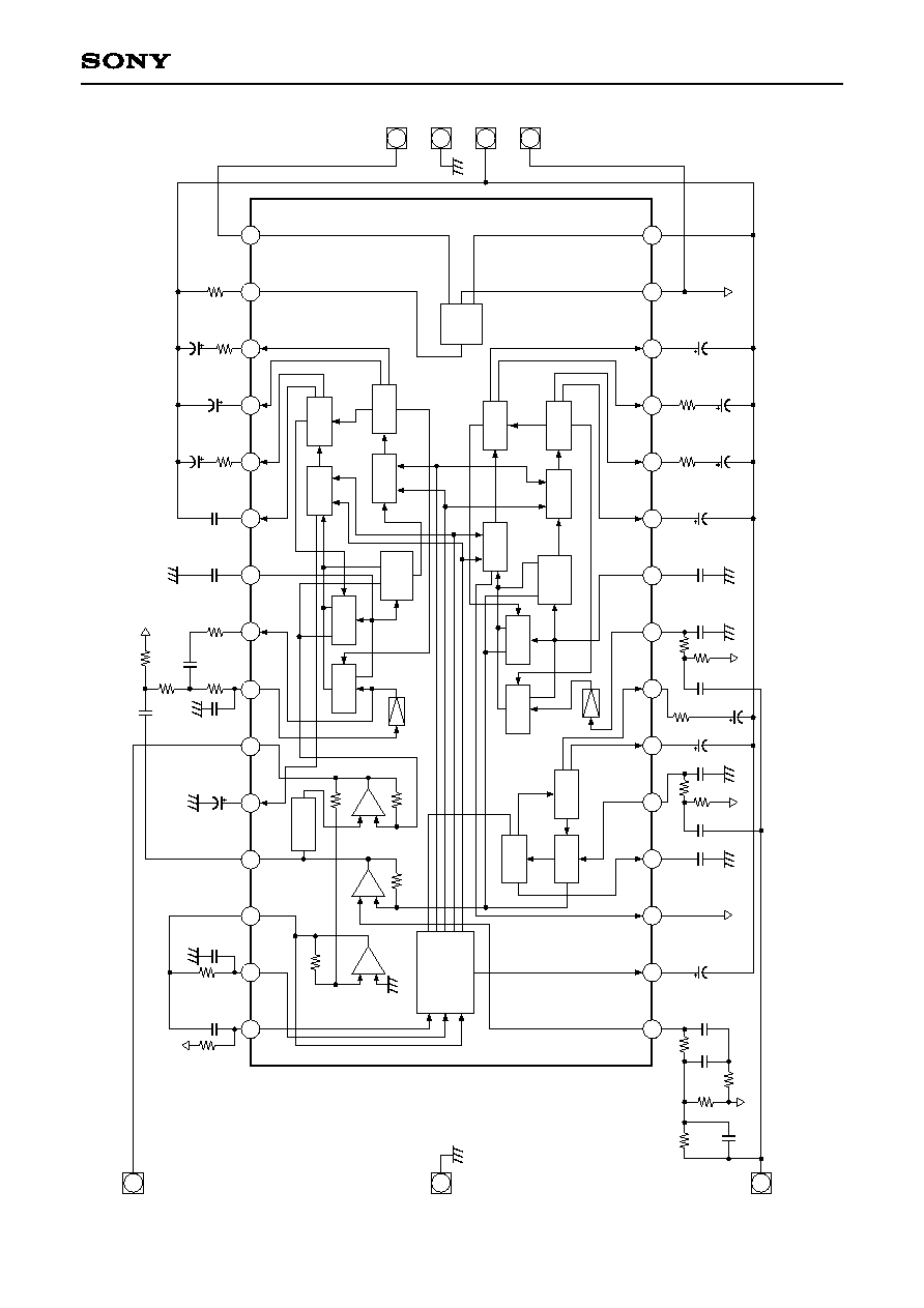
Block Diagram and Pin Configuration (Encoder Unit)
C30
2.2n
C25
39n
R31
13k
2%
R34
1.5k
R30
8.2k
2%
R27
10k
2%
C34
8.2n
C40
47n
C42
0.22µ
10%
R28
24k
2%
C44
0.1µ
C45
0.47µ
10%
C48
0.1µ
10%
C46
0.22µ
10%
C43
0.47µ
10%
C41
0.1µ
C31
8.2n
C29
470p
GND
RECOUT
GND
INPUT
MC
MC4
MC3
MC1
20k
15k
17.5k
20k
ANTSAT
FLVCR
SLVCR
V to I
Conv H
SLDET
SLICG
FLDET
FLICG
SHDET
V to I
Conv H
SHVCR
FHVCR
FHDET
FHICG
SHICG
V
REF
&
I
REF
LFDET
LFVCR
LFICG
V
EE
V
CC
VCT
VCT
VCT
VCT
VCT
R12
10k
C14
100n
C8
22n
R9
39k
VCT
R26
18k 2%
39k 2%
C27
680p
R24
10k 2%
C24 39n
C26 1µ
10%
C23 0.22µ
C20 22n
R16 39k 2%
C17 100n
C7
100n
C16
0.22µ
C21
1.8n
VCT
R20
5.1k 2%
R14 16k 2%
C11
100n
R15
2.4k 2%
R10
27k
2%
C19
1.8n
5
16
17
18
19
20
21
22
23
24
25
26
27
28
29
30
6
7
2
3
4
5
6
7
8
9
10
11
12
13
14
15
1
2
1
3
4
R25 33
R45
47
R47
33
R46
33
R48
47
HLSMP
MCTC
ZHSH
ZL2
LFIN
TCL1
TCL2
SCINH
FBOH
TCF1H
TCF2H
TCS2H
TCS1H
VCT
V
EE
MC4IN
MC3IN
MCBO
HLSOUT
ZHSL
RECOUT
SCINL
SCBOL
FBOL
TCS1L
TCS2L
TCF1L
TCF2L
IREF
V
CC
C38
1µ
MC4
MC3DS
MC3DT
MC2
MC1
VCT
R19
Note)
Split Supply: Short VCT to GND
Single Supply: Short GND to V
EE
and open VCT
Tolerances of resistors are 5% without otherwise specified
Tolerances of film capacitors are 5% without otherwise specified
Tolerances of chemical capacitors are 20% without otherwise specified
≠ 3 ≠
CXA1917AM/AS
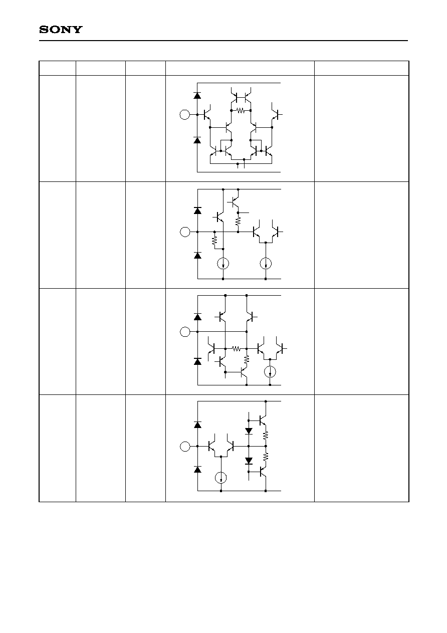
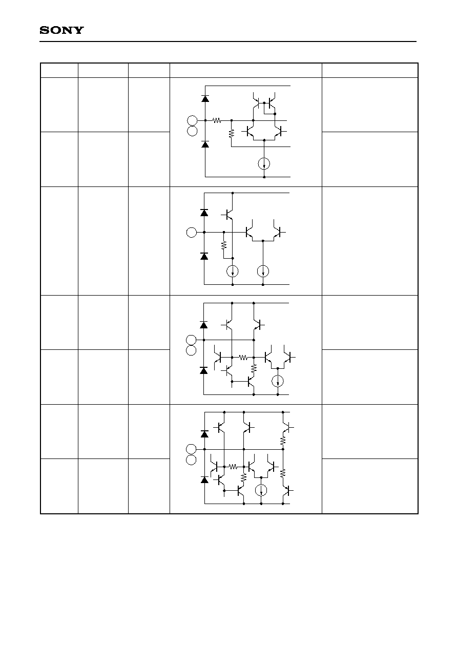
Pin Description
(DCV values are for Vcc = 6.0V and V
EE
= ≠6.0V.)
Pin No.
Symbol
DCV (V)
Equivalent Circuit
Description
1
HLSMP
0
HLS main path input
2
MCTC
≠3.9
Time constant for the
MC2
3
ZHSH
0
DC cut capacitance for
the HLS/HF/SB detector
4
ZL2
0
HF/LF/FB pass band
rectifier input
V
CC
V
EE
1
V
CC
V
EE
1.5k
9.2k
2p
2
V
CC
V
EE
2.6k
3
V
CC
GND
16k
VCT
4
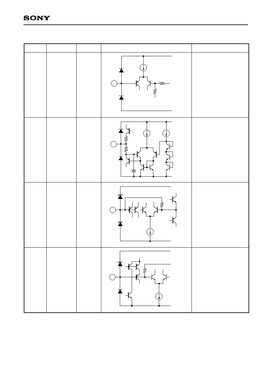
≠ 5 ≠
CXA1917AM/AS
9
FBOH
0
HLS/HF/FB VCR output
22
FBOL
0
LLS/HF/FB VCR output
10
TCF1H
0
Primary time constant for
the HLS/HF/FB detector
22
V
CC
GND
1.6k
5.1k
9
VCT
V
CC
80k
V
EE
10
18
V
CC
22k
V
EE
340k
11
20
V
CC
46k
V
EE
364k
2k
4k
12
11
TCF2H
≠4.6
Secondary time constant
for the HLS/HF/FB
detector
18
TCF2L
≠4.6
Secondary time constant
for the LLS/HF/FB
detector
12
TCS2H
≠4.6
Secondary time constant
for the HLS/HF/SB
detector
20
TCS2L
≠4.6
Secondary time constant
for the LLS/FB/SB
detector
Pin No.
Symbol
DCV (V)
Equivalent Circuit
Description