 | –≠–ª–µ–∫—Ç—Ä–æ–Ω–Ω—ã–π –∫–æ–º–ø–æ–Ω–µ–Ω—Ç: CXA1991N | –°–∫–∞—á–∞—Ç—å:  PDF PDF  ZIP ZIP |

--1--
E95925B8Y
Sony reserves the right to change products and specifications without prior notice. This information does not convey any license by
any implication or otherwise under any patents or other right. Application circuits shown, if any, are typical examples illustrating the
operation of the devices. Sony cannot assume responsibility for any problems arising out of the use of these circuits.
Absolute Maximum Ratings (Ta=25 ∞C)
∑ Supply voltage
V
CC
14
V
∑ Operating temperature
Topr
≠20 to +75
∞C
∑ Storage temperature
Tstg
≠65 to +150
∞C
∑ Allowable power dissipation
P
D
400
mW
Operating Conditions
Supply voltage
V
CC
1.8 to 4.5
V
Description
The CXA1991N is a tuner IC designed for use in
FM pagers and FM multiplex broadcasting. A
receiver system can be configured by using the
digital data output, in combination with a decoder. It
has a battery save function and ultra-low power
consumption.
Features
∑ Ultra-low power consumption
(I
D
= 1.2 mA for FM; I
D
= 0.8 mA for AM; V
CC
= 3 V)
∑ LED drive circuit for tuning
∑ Battery save function
∑ Few external parts
Applications
∑ Tuners for FM multiplex broadcasting
∑ FM pagers
FM Pager/FM Multiplex Tuner
20 pin SSOP (Plastic)
Block Diagram
1
2
3
4
5
6
7
8
9
10
20
19
18
17
16
15
14
12
11
AM FRONT END
FM FRONT END
13
REG
METER
BATTERY
SAVE CONT
FM IF DET
AM IF, IF DET
AGC
AGC BUFF
FE OUT
GND 1
FM IN
AM IN
FM RF
FM MIX
REG
FM OSC
AM OSC
TUNE
AM IF
AGC
FM IF
BAND
GND 2
DISCRI
V
CC
B.S
DET OUT
AFC
CXA1991N
For the availability of this product, please contact the sales office.

--2--
CXA1991N
Pin Description
(V
CC
=3 V, Ta=25 ∞C)
Pin
No.
1
2
9
3
4
5
6
7
Symbol
AM IF IN
AGC
DET OUT
FM IF IN
BAND
GND2
DISCRI
V
CC
Pin voltage (V)
FM
AM
1.1
1.1
0.3
0.4
0.9
0.7
1.1
0
1.1
0
0
0
2.0
2.4
3.0
3.0
Description
AM IF input pin.
Connected to a capacitor.
Detection output pin.
FM IF input pin.
AM/FM band switching pin.
AM when grounded, FM when
open.
IF system ground.
Connected to phase shift circuit
and ceramic discriminator.
Equivalent circuit
220k
1
330
3
4
V
CC
V
CC
2k
6
1.1k
V
CC
130
2
9
130 100k
--3--
CXA1991N
Equivalent circuit
200k
10
REG
13
V
CC
11
8
160k
550k
12
REG
V
CC
14
Pin
No.
8
10
13
11
12
14
Symbol
BS
AFC
FM OSC
TUNE
AM OSC
REG
Pin voltage (V)
FM
AM
1.0
0.7
1.1
1.1
1.1
1.1
1.1
1.1
1.1
1.1
Description
Controls battery save via
microcomputer.
High = Active, Low = Save
AFC varicap pin.
FM local oscillation circuit.
AM/FM tuning indicator drive
circuit.
AM local oscillation circuit.
Regulator output pin.

--4--
CXA1991N
Pin
No.
15
16
18
17
19
20
Symbol
FM MIX
FM RF
FM RF IN
AM RF IN
GND1
FE OUT
Pin voltage (V)
FM
AM
1.1
1.1
1.1
1.1
2.2
2.4
1.1
1.1
0
0
0.6
1.5
Equivalent circuit
Description
Load for mixer which resonates
at 10.7 MHz from internal
capacitance and external coil.
FM RF amplifier circuit which is
connected to RF tank circuit
FM RF amplifier circuit which is
FM RF input.
AM RF input which is
connected to bar antenna.
Front-end ground.
AM/FM IF output pin which is
connected to IF filter.
V
CC
5k
REG
18
16
50k
V
CC
FM Block
3k
20
15
AM Block
V
CC
17
V
CC
15
10k
REG
11p

--5--
CXA1991N
Current consumption
for FM no signal
Current consumption
for AM no signal
Current consumption
for battery save
FM front-end gain
FM detection
output level
FM IF knee level
FM detection
output distortion
IF center
frequency offset
FM meter current
AM front-end gain
AM IF gain
AM detection
output level
AM meter current
AM detection
output distortion
Bias and SW conditions
S1
S2
S3
S4
S5
OFF
OFF
OFF
OFF
OFF
ON
OFF
ON
ON
OFF
OFF
ON
ON
OFF
ON
ON
OFF
OFF
Measurement
item
OVER
BAND
BS
TUNE
FEOUT
Functional block
Input
point
--
--
--
V2
V3
V1
V4
V1
Measurement
point
A1
VA
VD
VB
9 pin-
14 pin
A2
VA
VD
VD
A2
VB
Standard Bias Conditions
Input waveform and
bias description
FM no signal
AM no signal
Vin=40 dB
µ
V,
100 MHz CW
Vin=90 dB
µ
V, 10.7 MHz
22.5 kHz DIV
Vin=90 dB
µ
V, 10.7 MHz
22.5 kHz DIV
Vin=90 dB
µ
V, 10.7 MHz
75 kHz DIV
Vin=90 dB
µ
V,
10.7 MHz CW
Vin=60 dB
µ
V,
10.7 MHz CW
Vin=75 dB
µ
V,
1660 kHz CW
Vin=455 kHz,
30 %mod
Vin=80 dB
µ
V,
455 kHz, 30 %
Vin=80 dB
µ
V,
455 kHz
Vin=100 dB
µ
V,
1660 kHz, 30 %
Output waveform and
measurement method description
10.7 MHz
V3 level when VB level for input of
V3 = 90 dB
µ
V drops by ≠3 dB.
Frequency offset from 10.7 MHz when Pin
9-Pin 14 DC potential difference is 0 mV.
455 kHz
VIN level for ≠40 dBm output.
1
2
3
4
5
6
7
8
9
10
11
12
13
14
MIN Limit
Min.
Typ.
Max.
Unit
0.60
1.25
1.90
mA
0.30
0.75
1.20
mA
--
--
1.00
µ
A
10
20
30
dB
39.0
73.5
123.5
mVrms
22.5
33.0
43.5
dB
µ
V
--
0.3
1.0
%
≠50
0
50
kHz
1.25
2.90
4.45
mA
25
28
31
dB
25.0
29.0
33.0
dB
µ
V
43.5
65.5
98.0
mVrms
1.50
2.9
4.30
mA
--
0.60
3.00
%
Electrical Characteristics
V
CC
=3 V, Ta=25
∞
C
Measurement No.
--6--
CXA1991N
FE OUT
GND 1
FM IN
AM IN
FM RF
FM MIX
REG
FM OSC
AM OSC
TUNE
AM IF
AGC
FM IF
BAND
GND 2
DISCRI
V
CC
B.S
DET OUT
AFC
0
.
4
7
µ
1
8
0
k
1
µ
2
0
k
0
.
0
1
µ
1
0
k
S
3
1
0
0
µ
0
.
1
µ
D
I
S
C
R
I
C
F
1
:
F
F
E
1
0
7
0
N
A
C
F
2
:
P
F
B
4
5
5
J
R
D
I
S
C
R
I
:
C
D
A
1
0
.
7
M
G
1
0
.
1
µ
S
2
1
µ
0
.
1
µ
0
.
1
µ
V
4
V
3
3
k
3
3
0
S
5
S
1
S
1
C
F
2
C
F
1
1
0
0
0
.
0
1
µ
1
5
0
µ
H
1
5
0
4
3
p
1
2
µ
H
3
0
p
3
3
p
S
4
1
0
µ
0
.
1
µ
V
2
V
1
S
w
i
t
c
h
m
o
d
e
O
N
O
F
F
V
C
A
2
B
P
F
V
A
A
1
V
B
V
D
1
2
3
4
5
6
7
8
9
1
0
2
0
1
9
1
8
1
7
1
6
1
5
1
4
1
2
1
1
1
3
3
0
p
3
9
p
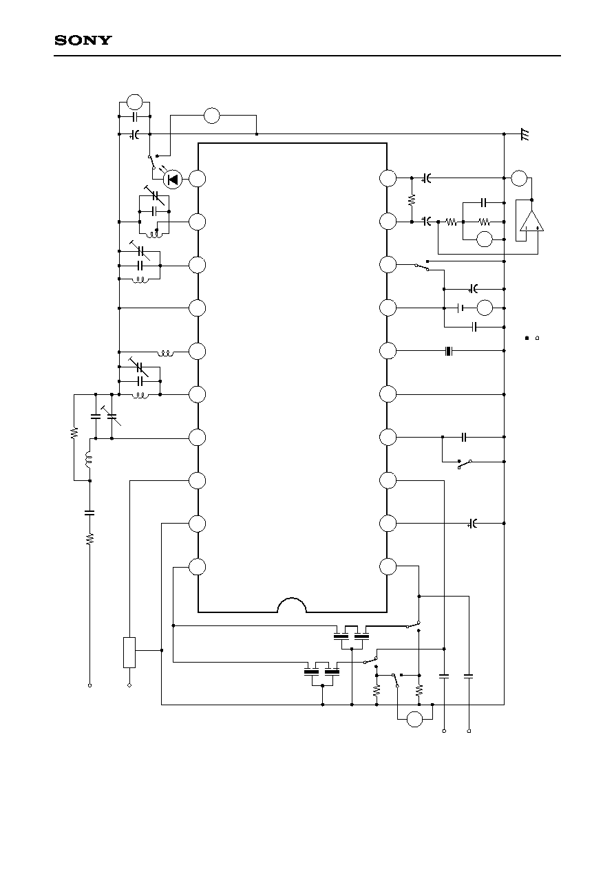
Electrical Characteristics Measurement Circuit

--7--
CXA1991N
Application Circuit
FE OUT
GND 1
FM IN
AM IN
FM RF
FM MIX
REG
FM OSC
AM OSC
TUNE
AM IF
AGC
FM IF
BAND
GND 2
DISCRI
V
CC
B.S
DET OUT
AFC
0
.
4
7
µ
1
8
0
k
1
µ
2
0
k
0
.
0
1
µ
1
0
k
S
2
0
.
1
µ
D
I
S
C
R
I
0
.
1
µ
1
µ
C
7
C
F
2
C
F
1
1
2
µ
H
1
0
µ
V
C
C
S
1
L
E
D
1
C
4
L
5
7
P
L
4
C
3
L
3
C
2
L
2
C
1
L
1
0
.
1
µ
C
6
F
M
A
M
C
8
1
0
0
µ
C
9
O
F
F
O
N
C
1
2
R
5
R
4
C
1
3
R
3
C
1
1
C
1
0
D
E
T
O
U
T
1
(
A
F
)
D
E
T
O
U
T
2
(
D
F
)
7
P
7
P
V
C
C
5
C
F
1
:
F
F
E
1
0
7
0
N
A
C
F
2
:
P
F
B
4
5
5
J
R
D
I
S
C
R
I
:
C
D
A
1
0
.
7
M
G
1
1
3
BP
F
7
8
9
1
0
6
5
4
2
3
1
2
0
1
8
1
2
1
7
1
4
1
1
1
5
1
6
1
9
Application circuits shown are typical examples illustrating the operation of the devices. Sony cannot assume responsibility for
any problems arising out of the use of these circuits or for any infringement of third party patent and other right due to same.
--8--
CXA1991N
≠50
O
u
t
p
u
t
l
e
v
e
l
r
a
t
i
o
[
d
B
]
Input level [dBµV]
≠40
≠30
≠20
≠10
0
≠60
0
≠10
10
20
30
40
50
60
70
80
90
100
110
N
≠2
≠3
≠4
≠1
T
.
H
.
D
.
-
T
o
t
a
l
h
a
r
m
o
n
i
c
d
i
s
t
o
r
t
i
o
n
[
%
]
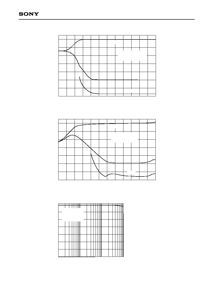
fc=100MHz
fs=1kHz, 22.5kHz dev.
V
CC
=3.0V
S+N
T.H.D
FM I/O characteristics (DET OUT 1)
≠50
O
u
t
p
u
t
l
e
v
e
l
r
a
t
i
o
[
d
B
]
Input level [dBµV]
≠40
≠30
≠20
≠10
0
≠60
0
≠10
10
20
30
40
50
60
70
80
90
100
110
S+N
N
T.H.D
≠2
≠3
≠4
≠1
T
.
H
.
D
.
-
T
o
t
a
l
h
a
r
m
o
n
i
c
d
i
s
t
o
r
t
i
o
n
[
%
]
fc=1660kHz
fs=1kHz, 30% mod.
V
CC
=3.0V
AM I/O characteristics (DET OUT 1)
≠10
DET OUT 2 frequency response
≠20
≠30
≠40
≠50
0
O
u
t
p
u
t
l
e
v
e
l
r
a
t
i
o
[
d
B
]
fs [Hz]
100
500 1k
5k 10k
50k 100k
V
CC
=3V
f
C
=10.7MHz
22.5kHz dev.
V
IN
=80dBµV

--9--
CXA1991N
Core diameter ¯ 0.06 2UEW
f [MHz]
1 to 3
2. 11
C [pF]
1 to 3
33
Q
1 to 3
40
Number of windings [t]
1 to 3
1 to 2
2 to 3
56
14
42
Equivalent to L7BRCS-1726Y TOKO Co., Ltd.
f [kHz]
L [µH]
Primary Secondary
Q
796
650
121t
22t
120
Core diameter ¯ 0.09 USTC
CF1
FFE1070NA
TDK Co., Ltd.
CF2
PFB455JR
Murata Mfg. Co., Ltd.
DISCRI
CDA10.7MG1
Murata Mfg. Co., Ltd.
VC
PVC2LXT16L
Mitsumi Electric Co., Ltd.
VC (Rear Mount)
HU22124N700
TOKO Co., Ltd.
PVC2LXT16B
Mitsumi Electric Co., Ltd.
4
6
1
3
AM OSC
S
2
Coil Data
FM OSC
4mm
0.6mm 3.5t
5mm
0.6mm 3.5t
FM RF
AM bar antenna
PRIMARY
SECONDARY
--10--
CXA1991N
Notes on Operation
1.De-emphasis time constant
Time constants are determined by R4, R5 and C13. The calculation formula is as follows.
{R4 ∑ R5/(R4 + R5)} ∑ C13
2.FM discriminator
Quadrature detection is used for FM detection. A ceramic resonator is used in the phase shifter so that no
adjustment is required. In order to eliminate problems of distortion and offset with IF band center
frequency, the CF1 (FM ∑ IF) and FM discrete pair combination should be of the same level.
3.Battery save function
The battery save function operates when Pin 8 is grounded. Current consumption is 1 µA or less during
battery save. To switch from battery save mode to normal mode, Pin 8 is connected to V
CC
. At this time
the DET OUT (Pin 9) rise time is affected by the rise time of Pins 4, 10 and 14. For faster rise time, lower
the capacitance values of bias capacitors C5, C6 and C8, taking care that characteristics do not
deteriorate. Also, decrease or eliminate R3 and C11 time constants and control Pin 10 directly with DC
voltage of approximately 1.1 V to improve rise time.
4.Notes on pattern preparation
i) FM antenna, OSC coil configuration
Change the direction 90 degrees in order to avoid M coupling. Also, insert Pin 14 pattern between
Pins 13 and 16 and the pattern between the coils. (See "Standard Board Diagram".)
ii) Tuning circuit
The capacitance value of the tuning circuit varies according to the board; investigate the time
constants for new boards.
iii) GND pins
Pin 5 is the ground pin for IF and Pin 19 is the ground pin for FE. Use as thick a pattern as possible
for the antenna input, BPF and Pin 19 grounds, as they have a significant effect on stability and NF
characteristics.
iv) The ground point for by-pass capacitors C5 and C6 connected to Pin 14 should be as close to Pin 14
as possible.
v) When the tuning indicator is not used, connect Pin 11 to ground. This will put the tuning indicator drive
circuit into low power consumption mode and current ceases to flow to the indicator. Also, the current
consumption I
CC
is eliminated.
vi) Use the BPF for FM.
CF1 and Discrete fo
A red
10.70 MHz
B blue
10.67 MHz
C orange
10.73 MHz
D black
10.64 MHz
E white
10.76 MHz
--11--
CXA1991N
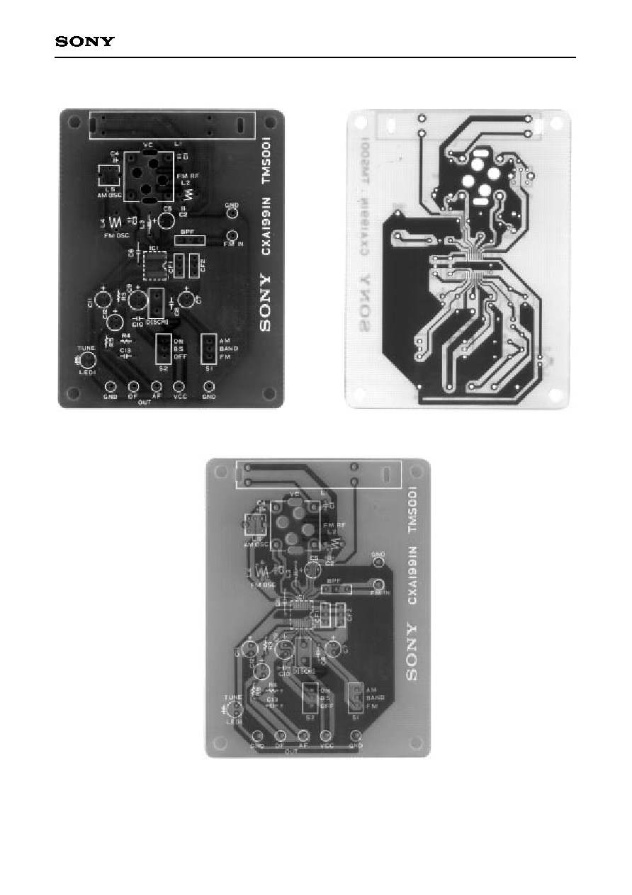
Standard Board Diagram
Component side symbols
Solder pattern side
Component pattern side

20PIN SSOP (PLASTIC)
SONY CODE
EIAJ CODE
JEDEC CODE
PACKAGE STRUCTURE
PACKAGE MATERIAL
LEAD TREATMENT
LEAD MATERIAL
PACKAGE MASS
EPOXY RESIN
SOLDER / PALLADIUM
42/COPPER ALLOY
0.1g
SSOP-20P-L01
SSOP020-P-0044
PLATING
0.1 ± 0.1
0
.
5
±
0
.
2
0∞ to 10∞
DETAIL A
NOTE: Dimension "
" does not include mold protrusion.
b=0.22 ≠ 0.05
+ 0.1
0
.
1
5
≠
0
.
0
2
+
0
.
0
5
(0.22)
(
0
.
1
5
)
0
.
1
5
≠
0
.
0
1
DETAIL B : SOLDER
DETAIL B : PALLADIUM
+
0
.
0
3
b=0.22 ± 0.03
6.5 ± 0.1
4
.
4
±
0
.
1
0.65
20
11
10
1
A
0.1
1.25 ≠ 0.1
+ 0.2
6
.
4
±
0
.
2
0.13 M
b
Package Outline Unit : mm
CXA1991N
--12--
NOTE : PALLADIUM PLATING
This product uses S-PdPPF (Sony Spec.-Palladium Pre-Plated Lead Frame).