 | ÐлекÑÑоннÑй компоненÑ: CXG1214UR | СкаÑаÑÑ:  PDF PDF  ZIP ZIP |
CXG1214UR(EF).fm
- 1 -
PE06133
Preliminary
This IC is ESD sensitive device. Special handling precautions are required.
Sony reserves the right to change products and specifications without prior notice. This information does not convey any license
by any implication or otherwise under any patents or other right. Application circuits shown, if any, are typical examples illustrating
the operation of the devices. Sony cannot assume responsibility for any problems arising out of the use of these circuits.
Preliminary
CXG1214UR
High Power 3P3T Switch with Logic Control
Description
The CXG1214UR is a 3P3T(Triple Pole Triple Throw) switch and suitable for wireless communication systems,
for example, W-CDMA handsets.
This IC has on-chip logic for operation with 3 COMS control inputs.
Low insertion loss and on-chip logic circuit are realized by the Sony JPHEMT process.
(Applications: Antenna switch for cellular handsets, triple band W-CDMA)
Features
Low insertion loss: 0.25dB@900MHz
3 CMOS compatible control line
Package
Small package size: 20-pin UQFN
Structure
GaAs JPHEMT MMIC
Absolute Maximum Ratings
(Ta = 25
°
C)
Bias voltage
V
DD
7
V
Control voltage
Vctl
5
V
Operating temperature
Topr
35 to +85
°
C
Storage temperature
Tstg
65 to +150
°
C

CXG1214UR
- 2 -
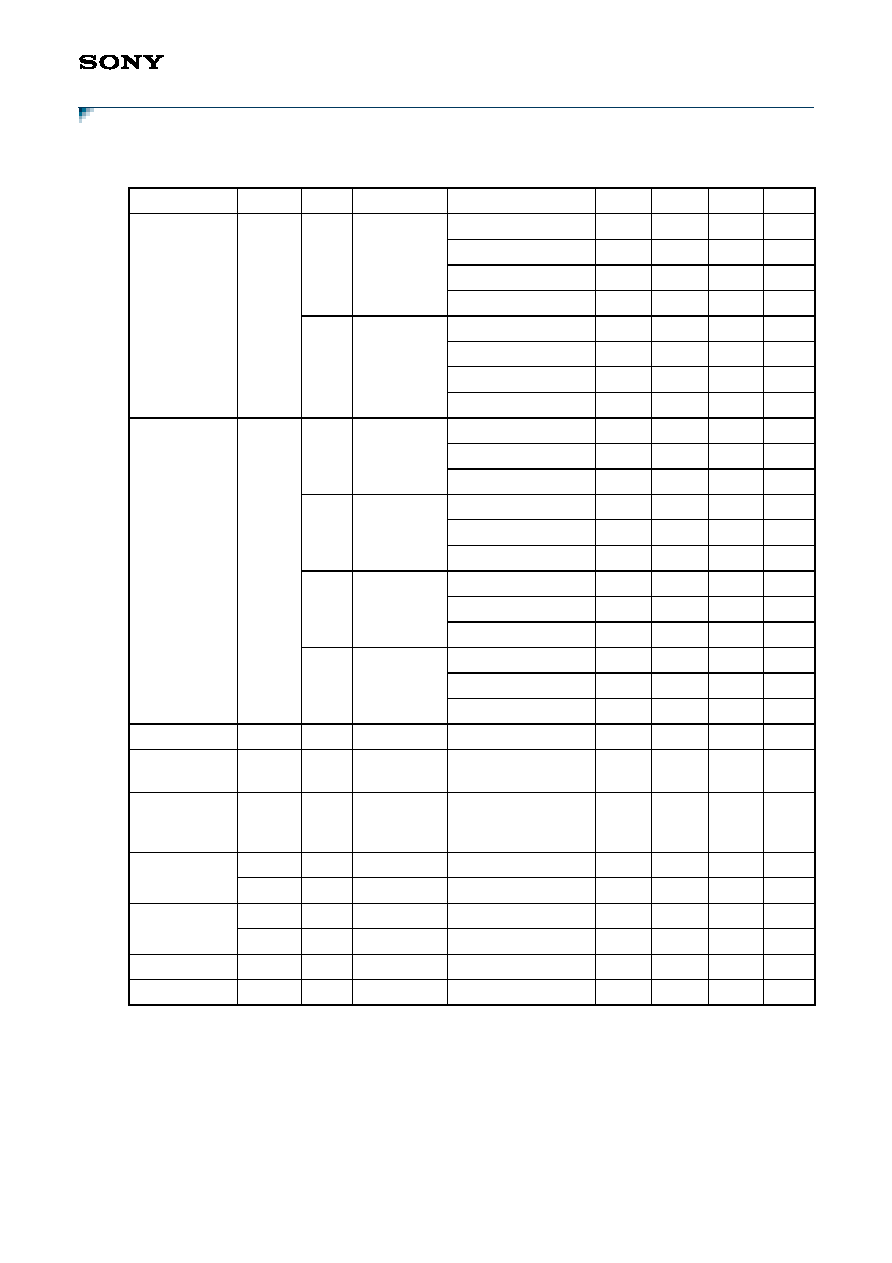
Block Diagram and Recommended Circuit
When using this IC, the following external components should be used:
C
RF
: This capacitor is used for RF decoupling and must be used for all applications.
Cbypass: This capacitor is used for DC line filtering.
Truth Table
DC Bias Conditions
(Ta = 25
°
C)
Cbypass
(100pF)
7
6
10
5
15
GND
14
RF3 (Band1)
13
GND
11
GND
CTLB
CTLC
V
DD
CTLA
GND
EXT
16
GND
RF2 (Band3)
GND3
19
ANT1
3
GND2 (Band 3)
2
GND
1
ANT2
C
RF
4
GND1(Band1)
C
RF
18
C
RF
12
C
RF
RF1 (Band6)
C
RF
9
20
17
8
GND4
C
RF
F10
F8
F9
F3
F11
F4
F2
F1
F5
F6
F7
F12
F13
State CTLA CTLB CTLC
ON path
F1
F2
F3
F4
F5
F6
F7
F8
F9 F10 F11 F12 F13
1
H
L
H
RF1 ANT1 ON OFF OFF OFF OFF OFF OFF ON ON OFF OFF ON ON
2
L
H
H
RF2 ANT2 OFF OFF ON OFF OFF OFF ON OFF ON OFF ON OFF ON
3
L
L
H
RF3 ANT2 OFF OFF OFF OFF ON OFF ON ON OFF ON OFF OFF ON
4
H
L
L
RF1 EXT OFF ON OFF OFF OFF OFF OFF ON ON OFF ON ON OFF
5
L
H
L
RF2 EXT OFF OFF OFF ON OFF OFF ON OFF ON OFF ON ON OFF
6
L
L
L
RF3 EXT OFF OFF OFF OFF OFF ON ON ON OFF ON ON ON OFF
Item
Min.
Typ.
Max.
Unit
Vctl (H)
2.2
2.85
3.2
V
Vctl (L)
0
--
0.4
V
V
DD
2.6
2.85
3.2
V
CXG1214UR
- 3 -
Electrical Characteristics
(Ta = 25
°
C)
*1
Pin = 25dBm, 0/2.85V control, V
DD
= 2.85V, 830 to 840MHz, 1749.9 to 1785MHz, 1920 to 1980MHz,
Mesurement system noise level : ACLR(
±
5MHz) <60dBc, (
±
10MHz) <65dBc, 2nd Harmonics <75dBm,
3rd Harmonics <75dBm
Item
Symbol
State
Path
Condition
Min.
Typ.
Max.
Unit
Insertion loss
IL
1
2
3
RF1 ANT1
RF2 ANT2
RF3 ANT2
830 to 885MHz
0.35
0.50
dB
1749.9 to 1880MHz
0.45
0.65
dB
1920 to 1980MHz
0.47
0.67
dB
2110 to 2170MHz
0.50
0.75
dB
4
5
6
RF1 EXT
RF2 EXT
RF3 EXT
830 to 885MHz
0.40
0.55
dB
1749.9 to 1880MHz
0.53
0.73
dB
1920 to 1980MHz
0.55
0.75
dB
2110 to 2170MHz
0.60
0.85
dB
Isolation
ISO
4
5
6
RF1 ANT1
RF2 ANT2
RF3 ANT2
830 to 885MHz
25
35
dB
1749.9 to 1880MHz
20
30
dB
1920 to 2170MHz
20
30
dB
1
RF1 EXT
830 to 885MHz
25
35
dB
1749.9 to 1880MHz
20
30
dB
1920 to 2170MHz
20
30
dB
2
RF2 EXT
830 to 885MHz
20
27
dB
1749.9 to 1880MHz
17
23
dB
1920 to 2170MHz
15
21
dB
3
RF3 EXT
830 to 885MHz
20
30
dB
1749.9 to 1880MHz
20
27
dB
1920 to 2170MHz
19
25
dB
VSWR
VSWR
50
1.2
Switching
speed
TSW
5
10
1dB
compression
input power
P1dB
V
DD
= 2.85V
32
dBm
ACLR
ACLR1
±
5MHz, 3.84MHz BW
*1
50
dBc
ACLR2
±
10MHz, 3.84MHz BW
*1
55
dBc
Harmonics
2fo
*1
45
dBm
3fo
*1
45
dBm
Bias current
Idd
V
DD
= 2.85V
200
330
µ
A
Control current Ictl
Vctl(H) = 2.85V
30
50
µ
A

CXG1214UR
- 4 -
Sony Corporation
Package Outline
(Unit: mm)
PIN 1 INDEX
C
0.1
S A-B
0.4
0.05 M
S
C
C
A-B
S
0.05 S
MAX0.02
+ 0.09
20PIN UQFN (PLASTIC)
0.25 0.03
+ 0.09
0.14 0.03
x 4
2.7
1
5
11
15
16
20
6
10
2.7
S
0.4 ± 0.1
1.3
0.55 ± 0.05
4-R0.3
0.26
A
B
0.25
0.14
0.07
0.18
SONY CODE
EIAJ CODE
JEDEC CODE
PACKAGE MATERIAL
LEAD TREATMENT
LEAD MATERIAL
EPOXY RESIN
SOLDER PLATING
COPPER ALLOY
0.02g
PACKAGE STRUCTURE
UQFN-20P-01
PACKAGE MASS
TERMINAL SECTION
Note:Cutting burr of lead are 0.05mm MAX.
Solder Plating
LEAD PLATING SPECIFICATIONS
ITEM
LEAD MATERIAL
COPPER ALLOY
SOLDER COMPOSITION
Sn-Bi Bi:1-4wt%
PLATING THICKNESS
5-18µm
SPEC.