
18Mb 1x1Dp, HSTL, rev 1.1
1 / 28
November 8, 2002
CXK79M72C164GB / CXK79M36C164GB
SONY
RAM
TM
33/4/5
18Mb 1x1Dp HSTL High Speed Synchronous SRAMs (256Kb x 72 or 512Kb x 36)
Preliminary
Description
The CXK79M72C164GB (organized as 262,144 words by 72 bits) and the CXK79M36C164GB (organized as 524,288 words
by 36 bits) are high speed CMOS synchronous static RAMs with common I/O pins. They are manufactured in compliance with
the JEDEC-standard 209 pin BGA package pinouts defined for SigmaRAM
TM
devices. They integrate input registers, high speed
RAM, output registers, and a two-deep write buffer onto a single monolithic IC. Single Data Rate (SDR) Pipelined (PL) read
operations and Double Late Write (DLW) write operations are supported, providing a high-performance user interface. Positive
and negative output clocks are provided for applications requiring source-synchronous operation.
All address and control input signals are registered on the rising edge of the CK differential input clock.
During read operations, output data is driven valid once, from the rising edge of CK, one full cycle after the address and control
signals are registered.
During write operations, input data is registered once, on the rising edge of CK, two full cycles after the address and control
signals are registered.
Output drivers are series-terminated, and output impedance is programmable via the ZQ control pin. When an external resistor
RQ is connected between ZQ and V
SS
, the impedance of the SRAM's output drivers is set to ~RQ/5.
300 MHz operation (300 Mbps) is obtained from a single 1.8V power supply. JTAG boundary scan interface is provided using
a subset of IEEE standard 1149.1 protocol.
Features
�
3 Speed Bins
Cycle Time / Data Access Time
-33
3.3ns / 1.8ns
-4
4.0ns / 2.1ns
-5
5.0ns / 2.3ns
� Single 1.8V power supply (V
DD
): 1.7V (min) to 1.95V (max)
� Dedicated output supply voltage (V
DDQ
): 1.4V (min) to V
DD
(max)
� HSTL-compatible I/O interface with dedicated input reference voltage (V
REF
): V
DDQ
/2 typical
� Common I/O
� Single Data Rate (SDR) data transfers
� Pipelined (PL) read operations
� Double Late Write (DLW) write operations
� Burst capability with internally controlled Linear Burst address sequencing
� Burst length of two, three, or four, with automatic address wrap
� Full read/write data coherency
� Byte write capability
� Differential input clocks (CK and CK)
� Data-referenced output clocks (CQ1, CQ1, CQ2, CQ2)
� Programmable output driver impedance via dedicated control pin (ZQ)
� Depth expansion capability (2 or 4 banks) via programmable chip enables (E2, E3, EP2, EP3)
� JTAG boundary scan (subset of IEEE standard 1149.1)
� 209 pin (11x19), 1mm pitch, 14mm x 22mm Ball Grid Array (BGA) package

SONY
�
RAM
CXK79M72C164GB / CXK79M36C164GB
Preliminary
18Mb 1x1Dp, HSTL, rev 1.1
2 / 28
November 8, 2002
256Kb x 72 Pin Assignment (Top View)
1
2
3
4
5
6
7
8
9
10
11
A
DQg
DQg
A
E2
A
ADV
A
E3
A
DQb
DQb
B
DQg
DQg
Bc
Bg
NC
(x36)
W
A
Bb
Bf
DQb
DQb
C
DQg
DQg
Bh
Bd
NC
(144M)
E1
NC
Be
Ba
DQb
DQb
D
DQg
DQg
V
SS
V
REF
NC
MCL
NC
V
REF
V
SS
DQb
DQb
E
DQg
DQc
V
DDQ
V
DDQ
V
DD
V
DD
V
DD
V
DDQ
V
DDQ
DQf
DQb
F
DQc
DQc
V
SS
V
SS
V
SS
ZQ
V
SS
V
SS
V
SS
DQf
DQf
G
DQc
DQc
V
DDQ
V
DDQ
V
DD
EP2
V
DD
V
DDQ
V
DDQ
DQf
DQf
H
DQc
DQc
V
SS
V
SS
V
SS
EP3
V
SS
V
SS
V
SS
DQf
DQf
J
DQc
DQc
V
DDQ
V
DDQ
V
DD
MCH
V
DD
V
DDQ
V
DDQ
DQf
DQf
K
CQ2
CQ2
CK
CK
V
SS
MCL
V
SS
NC
NC
CQ1
CQ1
L
DQh
DQh
V
DDQ
V
DDQ
V
DD
MCH
V
DD
V
DDQ
V
DDQ
DQa
DQa
M
DQh
DQh
V
SS
V
SS
V
SS
MCL
V
SS
V
SS
V
SS
DQa
DQa
N
DQh
DQh
V
DDQ
V
DDQ
V
DD
MCH
V
DD
V
DDQ
V
DDQ
DQa
DQa
P
DQh
DQh
V
SS
V
SS
V
SS
MCL
V
SS
V
SS
V
SS
DQa
DQa
R
DQd
DQh
V
DDQ
V
DDQ
V
DD
V
DD
V
DD
V
DDQ
V
DDQ
DQa
DQe
T
DQd
DQd
V
SS
V
REF
NC
MCL
NC
V
REF
V
SS
DQe
DQe
U
DQd
DQd
NC
A
NC
(72M)
A
NC
(36M)
A
NC
DQe
DQe
V
DQd
DQd
A
A
A
A1
A
A
A
DQe
DQe
W
DQd
DQd
TMS
TDI
A
A0
A
TDO
TCK
DQe
DQe

SONY
�
RAM
CXK79M72C164GB / CXK79M36C164GB
Preliminary
18Mb 1x1Dp, HSTL, rev 1.1
3 / 28
November 8, 2002
512Kb x 36 Pin Assignment (Top View)
1
2
3
4
5
6
7
8
9
10
11
A
NC
NC
A
E2
A
ADV
A
E3
A
DQb
DQb
B
NC
NC
Bc
NC
A
(x36)
W
A
Bb
NC
DQb
DQb
C
NC
NC
NC
Bd
NC
(144M)
E1
NC
NC
Ba
DQb
DQb
D
NC
NC
V
SS
V
REF
NC
MCL
NC
V
REF
V
SS
DQb
DQb
E
NC
DQc
V
DDQ
V
DDQ
V
DD
V
DD
V
DD
V
DDQ
V
DDQ
NC
DQb
F
DQc
DQc
V
SS
V
SS
V
SS
ZQ
V
SS
V
SS
V
SS
NC
NC
G
DQc
DQc
V
DDQ
V
DDQ
V
DD
EP2
V
DD
V
DDQ
V
DDQ
NC
NC
H
DQc
DQc
V
SS
V
SS
V
SS
EP3
V
SS
V
SS
V
SS
NC
NC
J
DQc
DQc
V
DDQ
V
DDQ
V
DD
MCH
V
DD
V
DDQ
V
DDQ
NC
NC
K
CQ2
CQ2
CK
CK
V
SS
MCL
V
SS
NC
NC
CQ1
CQ1
L
NC
NC
V
DDQ
V
DDQ
V
DD
MCH
V
DD
V
DDQ
V
DDQ
DQa
DQa
M
NC
NC
V
SS
V
SS
V
SS
MCL
V
SS
V
SS
V
SS
DQa
DQa
N
NC
NC
V
DDQ
V
DDQ
V
DD
MCH
V
DD
V
DDQ
V
DDQ
DQa
DQa
P
NC
NC
V
SS
V
SS
V
SS
MCL
V
SS
V
SS
V
SS
DQa
DQa
R
DQd
NC
V
DDQ
V
DDQ
V
DD
V
DD
V
DD
V
DDQ
V
DDQ
DQa
NC
T
DQd
DQd
V
SS
V
REF
NC
MCL
NC
V
REF
V
SS
NC
NC
U
DQd
DQd
NC
A
NC
(72M)
A
NC
(36M)
A
NC
NC
NC
V
DQd
DQd
A
A
A
A1
A
A
A
NC
NC
W
DQd
DQd
TMS
TDI
A
A0
A
TDO
TCK
NC
NC
SONY
�
RAM
CXK79M72C164GB / CXK79M36C164GB
Preliminary
18Mb 1x1Dp, HSTL, rev 1.1
4 / 28
November 8, 2002
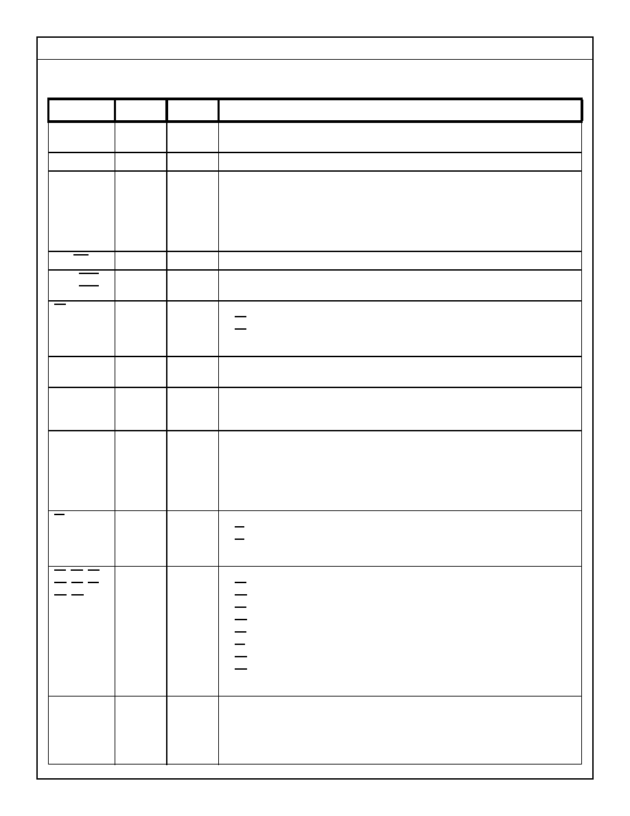
Pin Description
Symbol
Type
Quantity
Description
A
Input
x72 = 16
x36 = 17
Address Inputs - Registered on the rising edge of CK.
A1, A0
Input
2
Address Inputs 1,0 - Registered on the rising edge of CK. Initialize burst counter.
DQa, DQb
DQc, DQd
DQe, DQf
DQg, DQh
I/O
x72 = 72
x36 = 36
Data Inputs / Outputs - Registered on the rising edge of CK during write operations.
Driven from the rising edge of CK during read operations.
DQa - indicates Data Byte a
DQb - indicates Data Byte b
DQc - indicates Data Byte c
DQd - indicates Data Byte d
DQe - indicates Data Byte e
DQf - indicates Data Byte f
DQg - indicates Data Byte g
DQh - indicates Data Byte h
CK, CK
Input
2
Differential Input Clocks
CQ1, CQ1
CQ2, CQ2
Output
4
Output Clocks
E1
Input
1
Chip Enable Control Input - Registered on the rising edge of CK.
E1 = 0
enables the device to accept read and write commands.
E1 = 1
disables the device.
See the Clock Truth Table section for further information.
E2, E3
Input
2
Programmable Chip Enable Control Inputs - Registered on the rising edge of CK. See
the Clock Truth Table and Depth Expansion sections for further information.
EP2, EP3
Input
2
Programmable Chip Enable Active-Level Select Inputs - These pins must be tied
"high" or "low" at power-up. See the Clock Truth Table and Depth Expansion sec-
tions for further information.
ADV
Input
1
Address Advance Control Input - Registered on the rising edge of CK.
ADV = 0
loads a new address and begins a new operation when the device is
enabled.
ADV = 1
increments the address and continues the previous operation when the
device is enabled.
See the Clock Truth Table section for further information.
W
Input
1
Write Enable Control Input - Registered on the rising edge of CK.
W = 0
specifies a write operation when ADV = 0 and the device is enabled.
W = 1
specifies a read operation when ADV = 0 and the device is enabled.
See the Clock Truth Table section for further information.
Ba, Bb, Bc
Bd, Be, Bf
Bg, Bh
Input
x72 = 8
x36 = 4
Byte Write Enable Control Inputs - Registered on the rising edge of CK.
Ba = 0
specifies write Data Byte a during a write operation
Bb = 0
specifies write Data Byte b during a write operation
Bc = 0
specifies write Data Byte c during a write operation
Bd = 0
specifies write Data Byte d during a write operation
Be = 0
specifies write Data Byte e during a write operation
Bf = 0
specifies write Data Byte f during a write operation
Bg = 0
specifies write Data Byte g during a write operation
Bh = 0
specifies write Data Byte h during a write operation
See the Clock Truth Table section for further information.
ZQ
Input
1
Output Impedance Control Resistor Input - This pin must be tied to V
SS
through an
external resistor RQ at power-up. Output driver impedance is set to one-fifth the
value of RQ, nominally. See the Output Driver Impedance Control section for further
information.

SONY
�
RAM
CXK79M72C164GB / CXK79M36C164GB
Preliminary
18Mb 1x1Dp, HSTL, rev 1.1
5 / 28
November 8, 2002
V
DD
14
1.8V Core Power Supply - Core supply voltage.
V
DDQ
24
Output Power Supply - Output buffer supply voltage.
V
REF
4
Input Reference Voltage - Input buffer threshold voltage.
V
SS
30
Ground
TCK
Input
1
JTAG Clock
TMS
Input
1
JTAG Mode Select - Weakly pulled "high" internally.
TDI
Input
1
JTAG Data In - Weakly pulled "high" internally.
TDO
Output
1
JTAG Data Out
MCL
*Input*
5
Must Connect "Low" - May not be actual input pins.
MCH
*Input*
3
Must Connect "High" - May not be actual input pins.
NC
x72 = 13
x36 = 52
No Connect - These pins are true no-connects, i.e. there is no internal chip connection
to these pins. They can be left unconnected or tied directly to V
SS
.
Symbol
Type
Quantity
Description