 | –≠–ª–µ–∫—Ç—Ä–æ–Ω–Ω—ã–π –∫–æ–º–ø–æ–Ω–µ–Ω—Ç: CXN1010 | –°–∫–∞—á–∞—Ç—å:  PDF PDF  ZIP ZIP |

≠ 1 ≠
E03Y34A53
Sony reserves the right to change products and specifications without prior notice. This information does not convey any license by
any implication or otherwise under any patents or other right. Application circuits shown, if any, are typical examples illustrating the
operation of the devices. Sony cannot assume responsibility for any problems arising out of the use of these circuits.
CXN1010
Description
The CXN1010 is a fully integrated Class 2 radio and baseband module conforming to ver. 1.1 of the Bluetooth
specification.
Features
∑ UART, USB, PCM codec, PIO, and AIO interfaces, enabling a wide range of applications.
∑ Small package: 10
◊ 14 ◊ 1.5mm
∑ 8M-bit on-module flash memory
∑ Voltage regulator options: either on-module or external 1.8V regulator supported
∑ Based on the CXD3251GL, fully compatible with the Bluecore2-EXT from CSR
∑ Support for up to 7 slaves from a single master
∑ Channel quality driven data rate
General Specifications
∑ Product name:
Bluetooth
module
∑ Antenna connector impedance:
50
∑ External interfaces:
UART, USB, PCM, PIO, AIO
∑ Supply voltage:
2.3 to 3.6V
∑ Package dimensions:
10.0
◊ 14.0 ◊ 1.5mm
An external 1.75 V power supply is required for modules without internal voltage regulator (customer option).
Bluetooth
Module
Bluetooth
is a trademark owned by Bluetooth SIG, Inc. and licensed to Sony.
+0.15
≠0.05
R
R
R
R
≠ 2 ≠
CXN1010
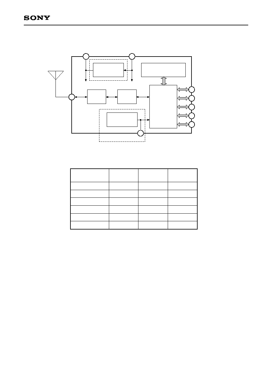
Block Diagram
[Option 2]
Regulator
[Option 1]
32MHz
32MHz_IN
BPF
Balun
Flash Memory
(8M-bit only)
BC2-Ext
UART
V
DD
: 3V
USB
PCM
SPI
PIO, AIO
V
DD
: 1.8V
ANT
V
DD
: 3V
V
DD
: 1.8V
TX
RX
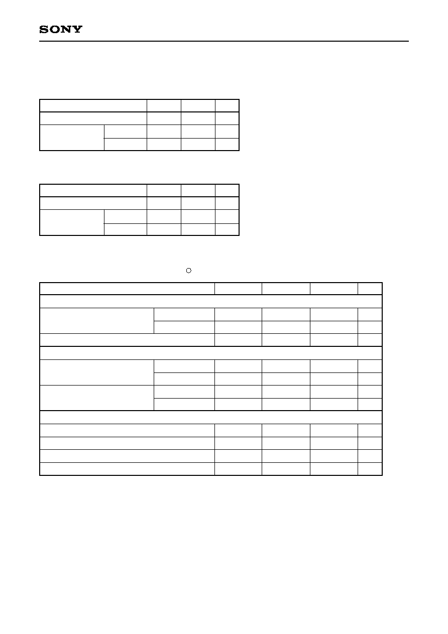
Module type
CXN1010-3AAL
CXN1010-2BAL
CXN1010-3BAL
CXN1010-3CAL
CXN1010-2DAL
CXN1010-3DAL
[Option 1]
X'tal
Mount
Mount
Mount
No mount
No mount
No mount
[Option 2]
Regulator
Mount
No mount
No mount
Mount
No mount
No mount
Supply V
DD
3V only
1.8V only
1.8V & 3V
3V only
1.8V only
1.8V & 3V

≠ 3 ≠
CXN1010
Pin Description
Pin Configuration (Top View)
1
2
3
4
5
6
7
8
9
10
11
12
32
31
30
29
28
27
26
25
24
23
22
13
40
14
39
15
38
16
37
17
36
18
35
19
34
20
33
21
No.
Name
Type
Description
1
2
3
4
5
6
7
8
9
10
11
12
13
14
15
GND
RF
GND
PIO_4/
USB_ON
PIO_3/
USB_WAKE_UP
PIO_6
PIO_8
32MHz_IN
PIO_7
SPI_MISO
PIO_9
CE
GND
SPI_CLK
V
DD
3.0
GND
Analog
GND
Bi-directional with programmable
weak internal pull-up/down
Bi-directional with programmable
weak internal pull-up/down
Bi-directional with programmable
weak internal pull-up/down
Bi-directional with programmable
weak internal pull-up/down
External clock input.
(Internal clock type is NC.)
Bi-directional with programmable
weak internal pull-up/down
CMOS output, tristatable with
weak internal pull-down
Bi-directional with programmable
weak internal pull-up/down
CMOS input
GND
CMOS input with weak internal
pull-down
V
DD
Ground.
RF input/output.
Ground.
Programmable I/O line or USB on.
Programmable I/O line or output goes high to
wake up PC when in USB mode.
Programmable I/O line.
Programmable I/O line.
External clock input.
A coupled capacitor is needed.
Programmable I/O line.
Serial Peripheral Interface data output.
Programmable I/O line.
1.8V regulator control.
Regulator on at high.
Ground.
Serial Peripheral Interface clock.
Supply voltage 3.0V.
This pin need a decoupling capacitor that more
than 2.2µF.

≠ 4 ≠
CXN1010
No.
Name
Type
Description
16
17
18
19
20
21
22
23
24
25
26
27
28
29
30
31
32
33
34
35
36
37
38
39
40
PIO_10
AIO_0
USB≠
AIO_1
USB+
GND
AIO_2
PIO_2
PIO_1
PD-RST
PIO_0
PIO_11
UART_RTS
UART_TX
UART_RX
PCM_IN
PCM_SYNC
GND
PCM_OUT
PCM_CLK
UART_CTS
SPI_MOSI
PIO_5/
USB_DETACH
SPI_CSB
V
DD
1.8
Bi-directional with programmable
weak internal pull-up/down
Bi-directional
Bi-directional
Bi-directional
Bi-directional
GND
Bi-directional
Bi-directional with programmable
weak internal pull-up/down
Bi-directional with programmable
weak internal pull-up/down
CMOS input with 1k
pull-down
Bi-directional with programmable
weak internal pull-up/down
Bi-directional with programmable
weak internal pull-up/down
CMOS output, tristatable with
weak internal pull-up
CMOS output
CMOS input with weak internal
pull-down
CMOS input with weak internal
pull-down
Bi-directional with 100k
pull-down
GND
CMOS output, tristatable with
weak internal pull-down
Bi-directional with weak internal
pull-down
CMOS input with weak internal
pull-down
Bi-directional with programmable
weak internal pull-up/down
CMOS input with weak internal
pull-up
CMOS input with weak internal
pull-down
V
DD
Programmable I/O line.
Programmable I/O line.
USB data minus.
Programmable I/O line.
USB data plus.
Ground.
Programmable I/O line.
Programmable I/O line.
Programmable I/O line.
Reset at high.
Input is debounced, so this pin should be high
for 5ms or more to cause a reset.
Programmable I/O line.
Programmable I/O line.
Weak internal pull-up
UART request to send, active low.
UART data output, active high.
UART data input, active high.
PCM data input.
PCM data sync.
Ground.
PCM data output.
PCM data clock.
UART clear to send, active low.
Serial Peripheral Interface data input.
Programmable I/O line or chip detaches from
USB when this input is high.
Chip select for Serial Peripheral Interface,
active low.
Supply voltage 1.8V.
This pin need a decoupling capacitor that more
than 2.2µF.
≠ 5 ≠
CXN1010
Electrical Characteristics
Absolute Maximum Ratings
Item
Storage temperature
Supply voltage
Max.
+85
1.90
3.60
Min.
≠20
≠0.40
≠0.40
Unit
∞C
V
V
Recommended Operating Conditions
Item
Operating temperature range
Supply voltage
Max.
+85
1.90
3.60
Min.
≠20
1.70
2.30
Unit
∞C
V
V
Input/Output Terminal Characteristics
(Temperature: ≠20 to +85∞C)
This I/O pin characteristics is the Bluetooth IC specifications used internally of the CXN1010.
Digital Terminals
Input Voltage
V
IL
input logic level low
V
IH
input logic level high
Output Voltage
V
OL
output logic level low
(I
O
= 4.0mA)
V
OH
output logic level high
(I
O
= 4.0mA)
Input and Tristate Current with:
Weak pull-up
Weak pull-down
I/O pad leakage current
C
I
input capacitance
Unit
V
V
V
V
V
V
V
µA
µA
µA
pF
V
DD
1.8
V
DD
3.0
V
DD
1.8
V
DD
3.0
V
DD
3.0 = 3.0V
V
DD
1.8 = 1.8V
V
DD
3.0 = 3.0V
V
DD
1.8 = 1.8V
V
DD
3.0 = 3.0V
V
DD
1.8 = 1.8V
Typ.
--
--
--
--
≠1
1
0
--
Min.
≠0.4
≠0.4
0.7
◊ V
DD
3.0
--
--
V
DD
3.0 ≠ 0.2
V
DD
1.8 ≠ 0.4
≠5
0
≠1
2.5
Max.
0.8
0.4
V
DD
3.0 + 0.4
0.2
0.4
--
--
0
5
1
10
R