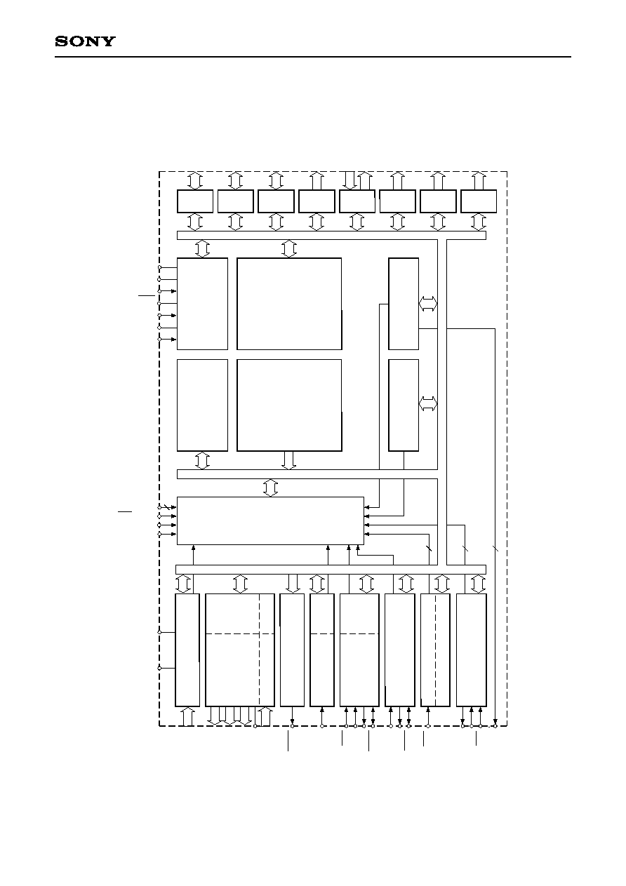
Description
The CXP82832/82840/82852/82860 is a CMOS 8-
bit single chip microcomputer integrating on a single
chip an A/D converter, serial interface, timer/counter,
time base timer, capture timer/counter, fluorescent
display panel controller/driver, remote control
reception circuit, and PWM output besides the basic
configurations of 8-bit CPU, ROM, RAM, and I/O port.
The CXP82832/82840/82852/82860 also provides
sleep/stop function that enables lower power
consumption.
Features
∑ Wide-range instruction system (213 instructions) to cover various types of data
-- 16-bit arithmetic/multiplication and division/boolean bit operation instructions
∑ Minimum instruction cycle
400ns at 10MHz operation
(122µs at 32kHz operation)
∑ Incorporated ROM capacity
32K bytes (CXP82832)
40K bytes (CXP82840)
52K bytes (CXP82852)
60K bytes (CXP82860)
∑ Incorporated RAM capacity
1536 bytes (including fluorescent display area)
∑ Peripheral functions
-- A/D converter
8 bits, 8 channels, successive approximation method
(Conversion time of 32µs/10MHz)
-- Serial interface
8-bit, 8-stage FIFO incorporated
(Auto transfer for 1 to 8 bytes), 1 channel
8-bit clock synchronized type, 1 channel
-- Timers
8-bit timer, 8-bit timer/counter, 19-bit time base timer
16-bit capture timer/counter, 32kHz timer/counter
-- Fluorescent display panel controller/driver
Supports the universal grid fluorescent display panel.
High voltage drive output port of 56 pins (40V)
Maximum of 640 segments display possible
Display timing number of 1 to 20
Dimmer function
Incorporated pull-down resistor (Mask option)
Hardware key scan function (Maximum of 16
◊
8 key matrix
supportable)
-- Remote control reception circuit
8-bit pulse measurement counter, 6-stage FIFO
-- PWM output
14 bits, 1 channel
∑ Interruption
16 factors, 15 vectors, multi-interruption possible
∑ Standby mode
SLEEP/STOP
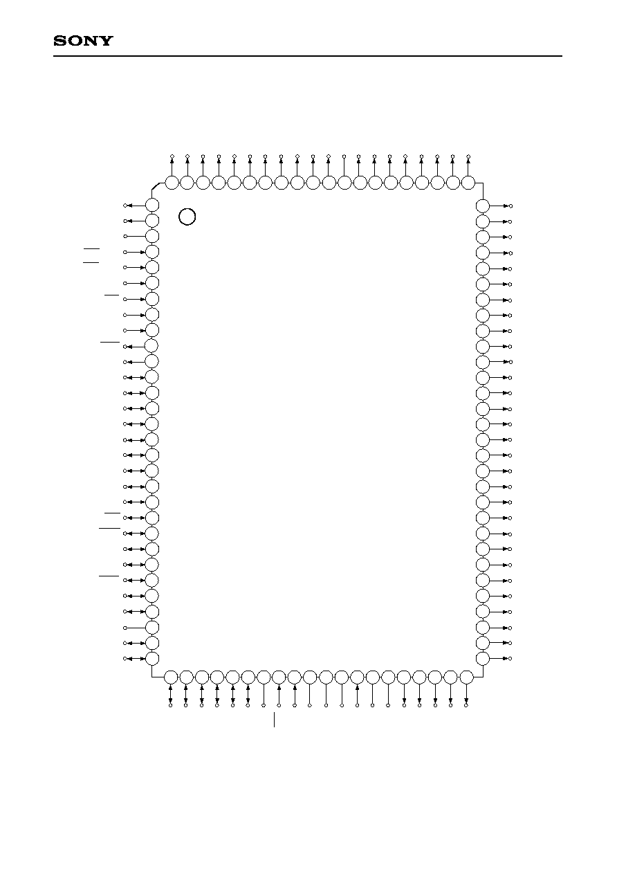
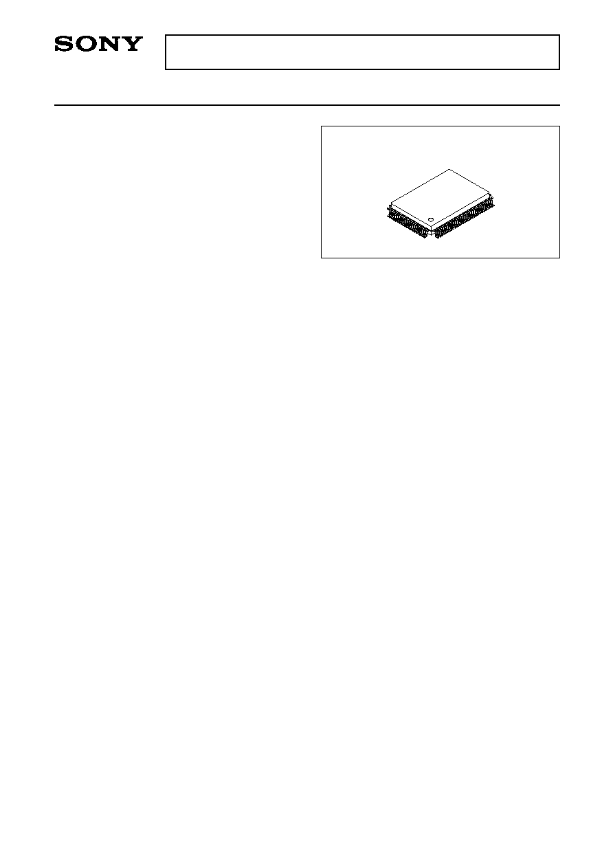
∑ Package
100-pin plastic QFP
∑ Piggyback/evaluation chip
CXP82800 100-pin ceramic QFP
Structure
Silicon gate CMOS IC
≠ 1 ≠
CXP82832/82840/82852/82860
E94Y08B74
CMOS 8-bit Single Chip Microcomputer
Sony reserves the right to change products and specifications without prior notice. This information does not convey any license by
any implication or otherwise under any patents or other right. Application circuits shown, if any, are typical examples illustrating the
operation of the devices. Sony cannot assume responsibility for any problems arising out of the use of these circuits.
100 pin QFP (Plastic)
≠ 4 ≠
CXP82832/82840/82852/82860
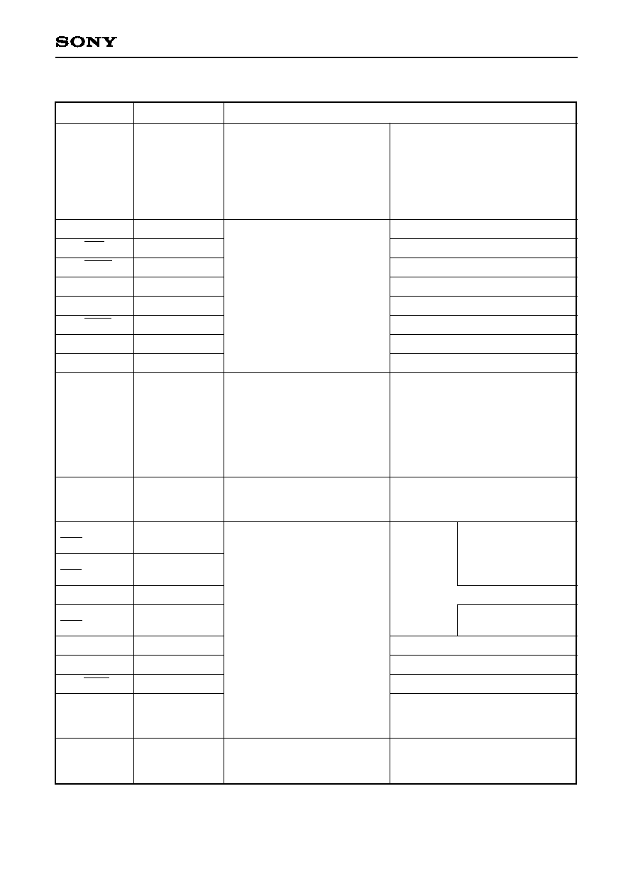
Pin Description
Pin code
I/O
Functions
I/O/
Analog input
PA0/AN0
to
PA7/AN7
(Port A)
8-bit I/O port. I/O can be set in a
unit of single bits. Incorporation
of the pull-up resistor can be set
through the software in a unit of
4 bits.
(8pins)
Analog inputs to A/D converter.
(8 pins)
I/O/Input
PC0/KR0
to
PC7/KR7
PE0/INT0/
EC0
PE1/INT1/
EC1
PE2/INT2
PE3/INT3/
NMI
PE4/RMC
PE5
PE6/PWM
PE7/TO/ADJ
PF0/A47
to
PF7/A40
Input/Input/Input
Input/Input/Input
Input/Input
Input/Input/Input
Input/Input
Input
Output/Output
Output/Output/
Output
Output/Output
(Port C)
8-bit I/O port. I/O can be set in a
unit of single bits. Can drive
12mA sync current.
Incorporation of the pull-up
resistor can be set through the
software in a unit of 4 bits.
(8 pins)
Serves as key return inputs when
operating key scan with fluorescent
display panel (FDP) segment signal.
(8 pins)
Output/Output
PD0/A55
to
PD7/A48
(Port D)
8-bit output port.
(8 pins)
FDP segment signal (anode
connection) outputs.
(Port E)
8-bit port. Lower 6 bits are for
inputs; upper 2 bits are for
outputs.
(8 pins)
(Port F)
8-bit output port.
(8pins)
External event inputs
for timer/counter.
(2 pins)
Inputs for
external
interruption
request.
(4 pins)
Non-maskable
interruption request input.
Remote control reception circuit input.
14-bit PWM output.
Output for the 16-bit timer/counter
rectangular waves, and 32kHz
oscillation frequency division.
FDP segment signal (anode
connection) outputs.
I/O/Input
I/O/Input
I/O/I/O
I/O/Input
I/O/Output
I/O/I/O
I/O/Input
I/O/Output
PB0/CINT
PB1/CS0
PB2/SCK0
PB3/SI0
PB4/SO0
PB5/SCK1
PB6/SI1
PB7/SO1
(Port B)
8-bit I/O port. I/O can be set in a
unit of single bits. Incorporation
of the pull-up resistor can be set
through the software in a unit of
4 bits.
(8 pins)
Capture input to 16-bit timer/counter.
Chip select input for serial interface (CH0).
Serial clock I/O (CH0).
Serial data input (CH0).
Serial data output (CH0).
Serial clock I/O (CH1).
Serial data input (CH1).
Serial data output (CH1).
≠ 5 ≠
CXP82832/82840/82852/82860
Pin code
I/O
Functions
Output
A16 to A23
FDP segment signal (anode connection) outputs.
(8 pins)
Output/Output
G0/A0
to
G15/A15
Outputs for FDP timing signals (grid connection)/segment signals (anode
connection).
(16 pins)
Output/Output
PH0/A31
to
PH7/A24
Output/Output
PG0/A39
to
PG7/A32
(Port H)
8-bit output port.
(8 pins)
V
FDP
EXTAL
XTAL
TEX
TX
RST
NC
AV
REF
AV
SS
V
DD
V
SS
Input
Output
Input
Output
Input
Input
FDP voltage supply when incorporated pull-down (PD) resistor is set by
mask option.
Crystal connectors for system clock oscillation. When the clock is
supplied externally, input to EXTAL; opposite phase clock should be
input to XTAL.
Crystal connectors for 32kHz timer/counter clock oscillation. For usage
as event input, input to TEX, and open TX.
Low-level active, system reset
NC. Under normal operation, connect to V
DD
.
Reference voltage input for A/D converter.
A/D converter GND.
V
CC
supply.
GND.
FDP segment signal (anode
connection) outputs.
(8 pins)
(Port G)
8-bit output port.
(8 pins)
FDP segment signal (anode
connection) outputs.
(8 pins)