 | –≠–ª–µ–∫—Ç—Ä–æ–Ω–Ω—ã–π –∫–æ–º–ø–æ–Ω–µ–Ω—Ç: CXP83409 | –°–∫–∞—á–∞—Ç—å:  PDF PDF  ZIP ZIP |
≠ 1 ≠
CXP83408/83412/83416
CXP83409/83413/83417
E93Z15C72-PS
CMOS 8-bit Single Chip Microcomputer
Description
The CXP83408/83412/83416 and CXP83409/83413/
83417 are a CMOS 8-bit microcomputer which consists of
A/D converter, serial interface, timer/counter, time
base timer, 32kHz timer/counter, LCD controller/
driver, remote control receiving circuit and PWM
output, as well as basic configurations like 8-bit CPU,
ROM, RAM and I/O port. They are integrated into a
single chip.
Also CXP83408/83412/83416 and CXP83409/83413/
83417 sleep/ stop function which enables to lower power
consumption.
Features
∑ A wide instruction set (213 instructions) which
covers various types of data
≠ 16-bit arithmetic/multiplication and division/
Boolean bit operation instructions
∑ Minimum instruction cycle
400ns at 10MHz operation (4.5 to 5.5V)
122µs at 32kHz operation (2.7 to 5.5V)
∑ Incorporated ROM capacity
8K bytes (CXP83408, 83409)
12K bytes (CXP83412, 83413)
16K bytes (CXP83416, 83417)
∑ Incorporated RAM capacity
448 bytes (LCD display data area included)
∑ Peripheral functions
≠ A/D converter
8 bits, 8 channels, successive approximation system
(Conversion time: 32µs/10MHz)
≠ Serial interface
Incorporated 8-bit and 8-stage FIFO
(1 to 8 bytes auto transfer), 1 circuit 2 channels
≠ Timer
8-bit timer, 8-bit timer/counter, 19-bit time base timer, 32kHz timer/counter
≠ LCD controller/driver
Maximum 128 segments display possible (During 1/4 duty)
4 common outputs, 32 segment outputs
Display method: Static, 1/2, 1/3 and 1/4 duty
Bias method: 1/2 and 1/3 bias
≠ Remote control receiving circuit
8-bit pulse measurement counter, 6-stage FIFO
≠ PWM output
14 bits 1 channel, 8 bits 1 channel
∑ Interruption
12 factors, 12 vectors, multi-interruption possible
∑ Standby mode
SLEEP/STOP
∑ Package
80-pin plastic QFP/LQFP
∑ Piggyback/evaluator
CXP83400 (CXP83408, 83412, 83416)
CXP83401 (CXP83409, 83413, 83417)
Structure
Silicon gate CMOS IC
Sony reserves the right to change products and specifications without prior notice. This information does not convey any license by
any implication or otherwise under any patents or other right. Application circuits shown, if any, are typical examples illustrating the
operation of the devices. Sony cannot assume responsibility for any problems arising out of the use of these circuits.
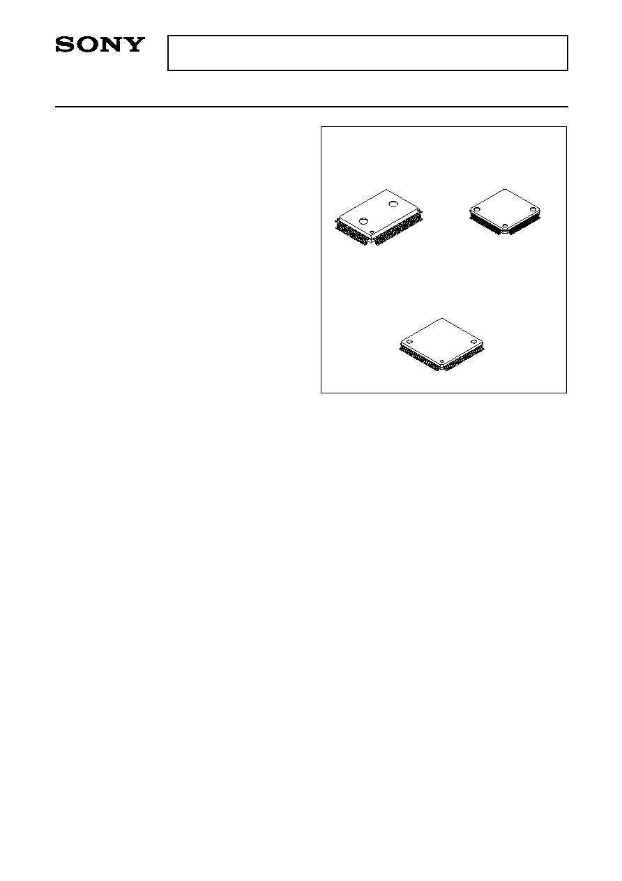
CXP83408/83412/83416
80 pin QFP (Plastic) 80 pin LQFP (Plastic)
CXP83409/83413/83417
80 pin QFP (Plastic)
≠ 2 ≠
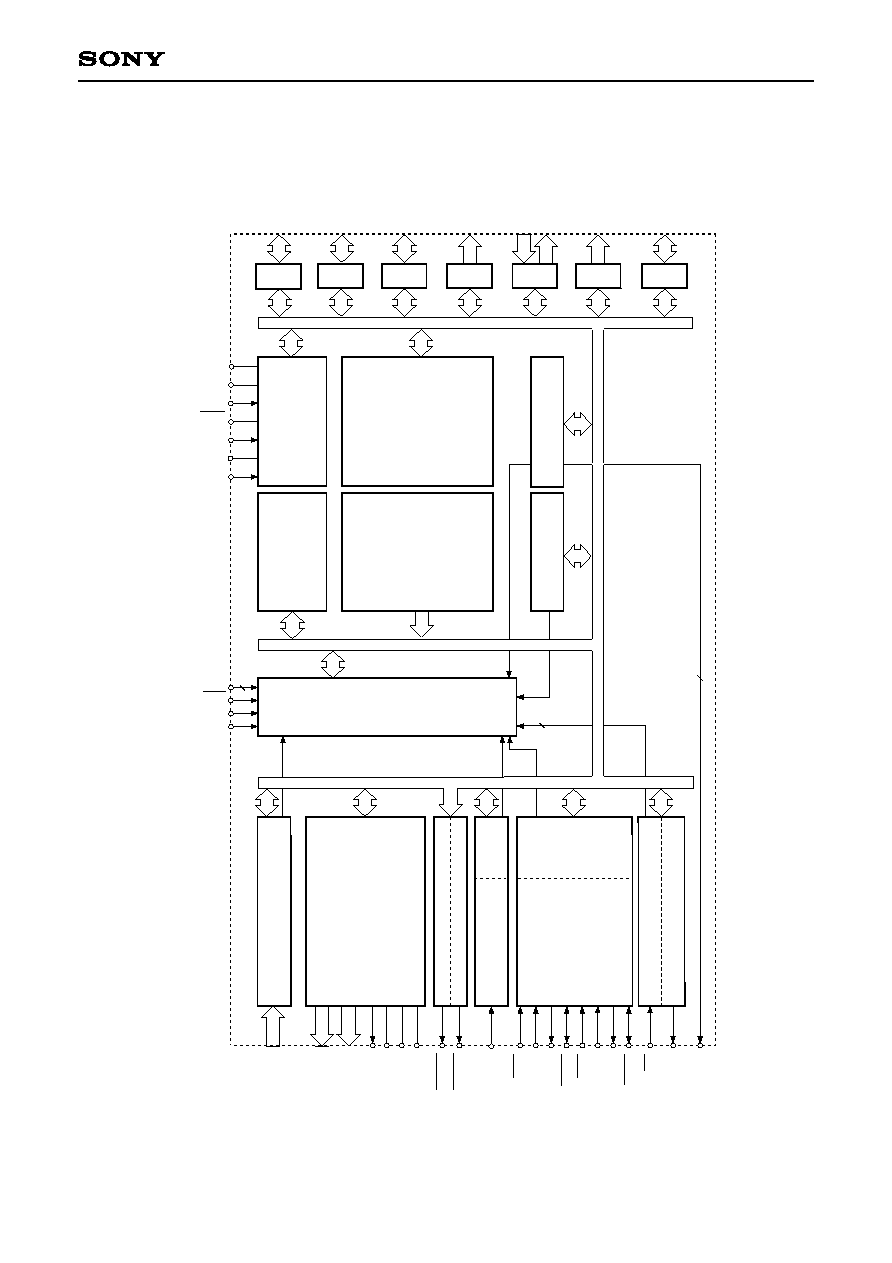
CXP83408/83412/83416, CXP83409/83413/83417
XTAL
A/D CONVERTER
14BIT PWM GENERATOR
REMOCON
SERIAL
INTERFACE
UNIT 0
8BIT TIMER/COUNTER 0
8BIT TIMER 1
FIFO
FIFO
INTERRUPT CONTROLLER
SPC700
CPU CORE
ROM
8K/12K/16K BYTES
PRESCALER/
TIME BASE TIMER
32kHz
TIMER/COUNTER
RAM
448 BYTES
8
AN0 to AN7
PWM0
RMC
SI0
SO0
SI1
SO1
EC
CS0
SCK0
SCK1
INT0
INT1
INT2
NMI/INT3
TEX
TX
EXTAL
V
DD
Vss
PORT C
8
PC0 to PC7
PORT H
1
PH0
PORT B
8
PB0 to PB7
PORT E
5
2
PE0 to PE4
PE5 to PE6
2
LCD
CONTROLLER/
DRIVER
32
SEG0 to SEG31
4
COM0 to COM3
V
L
V
LC1
V
LC2
PORT A
8
PA0 to PA7
PORT D
8
PD0 to PD7
PORT F
8
PF0 to PF7
V
LC3
ADJ
PWM1
8BIT PWM GENERATOR
CS1
TO
CLOCK GENERATOR/
SYSTEM CONTROL
RST
2
2
Block Diagram
≠ 3 ≠
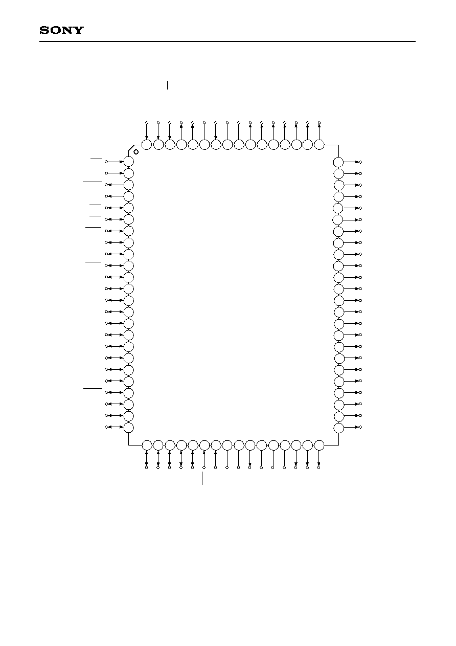
CXP83408/83412/83416, CXP83409/83413/83417
PE3/INT3/NMI
PE4/RMC
PE5/PWM0
PE6/TO/ADJ
PB0/CS1
PB1/CS0
PB2/SCK0
PB3/SI0
PB4/SO0
PB5/SCK1
PB6/SI1
PB7/SO1
PC0
PC1
PC2
PC3
PC4
PC5
PC6
PC7
PH0/PWM1
PA0/AN0
PA1/AN1
PA2/AN2
PD6/SEG22
PD5/SEG21
PD4/SEG20
PD3/SEG19
PD2/SEG18
PD1/SEG17
PD0/SEG16
SEG15
SEG14
SEG13
SEG12
SEG11
SEG10
SEG9
SEG8
SEG7
SEG6
SEG5
SEG4
SEG3
SEG2
SEG1
SEG0
COM3
PA3/AN3
PA4/AN4
PA5/AN5
PA6/AN6
PA7/AN7
RST
EXTAL
XTAL
V
SS
V
L
V
LC3
V
LC2
V
LC1
COM0
COM1
COM2
PE2/INT2
PE1/INT1
PE0/INT0/EC
PF7/SEG31
PF6/SEG30
NC
TEX
TX
V
DD
PF5/SEG29
PF4/SEG28
PF3/SEG27
PF2/SEG26
PF1/SEG25
PF0/SEG24
PD7/SEG23
2
3
4
5
6
7
8
9
10
11
12
13
14
15
16
17
18
19
20
21
22
23
24
25 26 27 28 29 30
40
39
38
37
36
35
34
31 32 33
70 69 68 67
65
66
71
72
73
74
75
76
77
78
79
80
1
41
42
43
44
45
46
47
48
49
50
51
52
53
54
55
56
57
58
59
60
63
64
61
62
Pin Assignment (Top View) CXP83408/83412/83416 (QFP package)
Note) NC (Pin 75) is always connected to V
DD
.

≠ 4 ≠
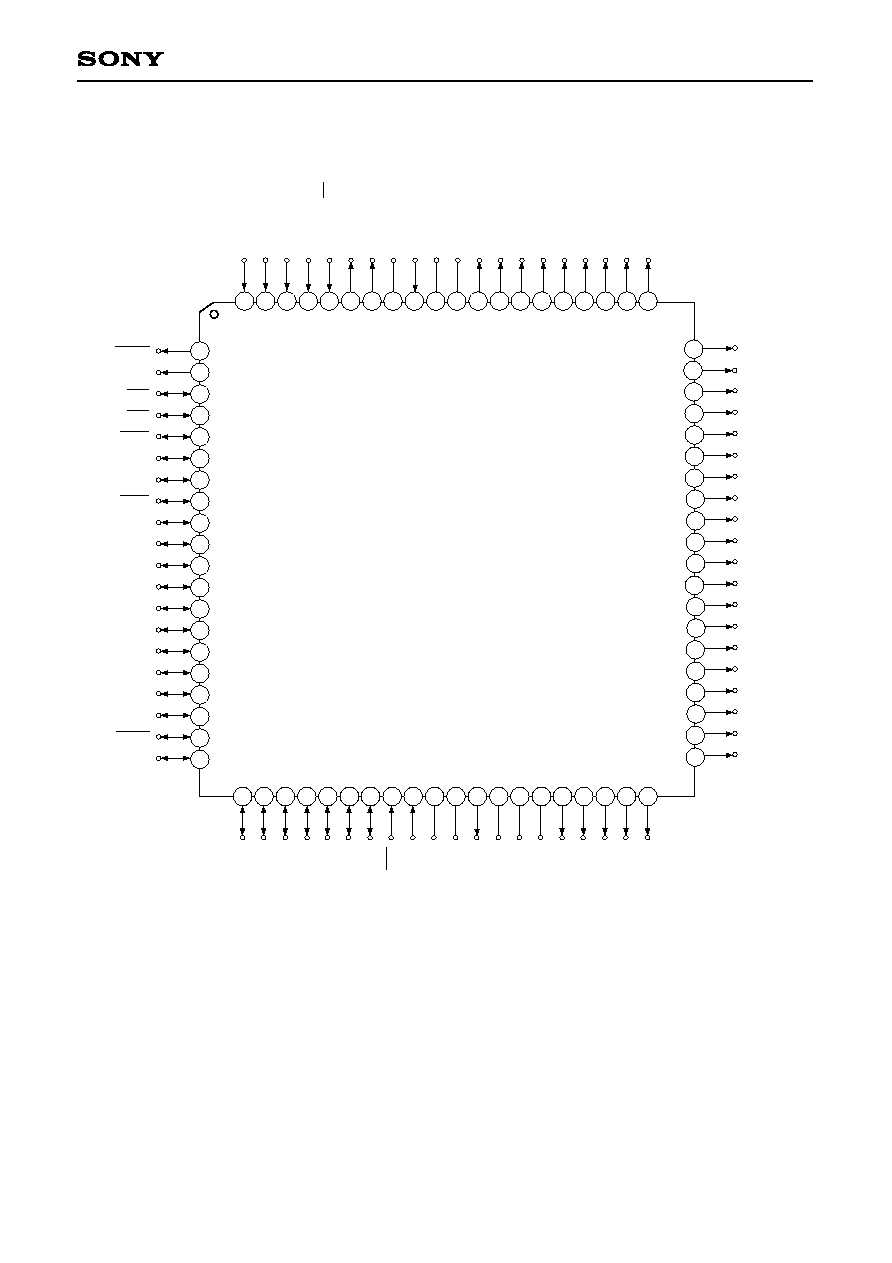
CXP83408/83412/83416, CXP83409/83413/83417
PE5/PWM0
PE6/TO/ADJ
PB0/CS1
PB1/CS0
PB2/SCK0
PB3/SI0
PB4/SO0
PB5/SCK1
PB6/SI1
PB7/SO1
PC0
PC1
PC2
PC3
PC4
PC5
PC6
PC7
PH0/PWM1
PA0/AN0
PD4/SEG20
PD3/SEG19
PD2/SEG18
PD1/SEG17
PD0/SEG16
SEG15
SEG14
SEG13
SEG12
SEG11
SEG10
SEG9
SEG8
SEG7
SEG6
SEG5
SEG4
SEG3
SEG2
SEG1
PA1/AN1
PA2/AN2
PA3/AN3
PA4/AN4
PA5/AN5
PA6/AN6
PA7/AN7
RST
EXTAL
XTAL
V
SS
V
L
V
LC3
V
LC2
V
LC1
COM0
COM1
COM2
COM3
SEG0
PE4/RMC
PE3/INT3/NMI
PE2/INT2
PE1/INT1
PE0/INT0/EC
PF7/SEG31
PF6/SEG30
NC
TEX
TX
V
DD
PF5/SEG29
PF4/SEG28
PF3/SEG27
PF2/SEG26
PF1/SEG25
PF0/SEG24
PD7/SEG23
PD6/SEG22
PD5/SEG21
2
3
4
5
6
7
8
9
10
11
12
13
14
15
16
17
18
19
20
21 22 23 24 25 26 27 28 29 30
40
39
38
37
36
35
34
31 32 33
70 69 68 67
65
66
71
72
73
74
75
76
77
78
79
80
1
41
42
43
44
45
46
47
48
49
50
51
52
53
54
55
56
57
58
59
60
63
64
61
62
Pin Assignment (Top View) CXP83408/83412/83416 (LQFP package)
Note) NC (Pin 73) is always connected to V
DD
.
≠ 5 ≠
CXP83408/83412/83416, CXP83409/83413/83417
PE5/PWM0
PE6/TO/ADJ
PB0/CS1
PB1/CS0
PB2/SCK0
PB3/SI0
PB4/SO0
PB5/SCK1
PB6/SI1
PB7/SO1
PC0
PC1
PC2
PC3
PC4
PC5
PC6
PC7
PH0/PWM1
PA0/AN0
PD4/SEG20
PD3/SEG19
PD2/SEG18
PD1/SEG17
PD0/SEG16
SEG15
SEG14
SEG13
SEG12
SEG11
SEG10
SEG9
SEG8
SEG7
SEG6
SEG5
SEG4
SEG3
SEG2
SEG1
PA1/AN1
PA2/AN2
PA3/AN3
PA4/AN4
PA5/AN5
PA6/AN6
PA7/AN7
RST
EXTAL
XTAL
V
SS
V
L
V
LC3
V
LC2
V
LC1
COM0
COM1
COM2
COM3
SEG0
PE4/RMC
PE3/INT3/NMI
PE2/INT2
PE1/INT1
PE0/INT0/EC
PF7/SEG31
PF6/SEG30
NC
TEX
TX
V
DD
PF5/SEG29
PF4/SEG28
PF3/SEG27
PF2/SEG26
PF1/SEG25
PF0/SEG24
PD7/SEG23
PD6/SEG22
PD5/SEG21
2
3
4
5
6
7
8
9
10
11
12
13
14
15
16
17
18
19
20
21 22 23 24 25 26 27 28 29 30
40
39
38
37
36
35
34
31 32 33
70 69 68 67
65
66
71
72
73
74
75
76
77
78
79
80
1
41
42
43
44
45
46
47
48
49
50
51
52
53
54
55
56
57
58
59
60
63
64
61
62
Pin Assignment (Top View) CXP83409/83413/83417 (QFP package)
Note) NC (Pin 73) is always connected to V
DD
.
≠ 6 ≠
CXP83408/83412/83416, CXP83409/83413/83417
Pin Description
Symbol
I/O
Functions
I/O/Analog input
PA0/AN0
to
PA7/AN7
(Port A)
8-bit I/O port. I/O can be
set in a unit of single bits.
Incorporation of pull-up
resistor can be set
through the software in a
unit of 4 bits.
(8 pins)
Analog inputs to A/D converter.
(8 pins)
I/O
PC0 to PC7
(Port C)
8-bit I/O port. I/O can be set in a unit of single bits. Capable of driving
12mA sync current. Incorporation of pull-up resistor can be set through
the software in a unit of 4 bits.
(8 pins)
I/O/Output
PH0/PWM1
(Port H)
1-bit I/O port. Incorporation
of pull-up resistor can be
set through the software.
(1 pin)
8-bit PWM output.
Input/Input/Input
Input/Input
Input/Input
Input/Input/Input
Input/Input
Output/Output
Output/Output/
Output
PE0/INT0/EC
PE1/INT1
PE2/INT2
PE3/INT3/NMI
PE4/RMC
PE5/PWM0
PE6/TO/ADJ
(Port E)
7-bit port. Lower 5 bits
are for inputs; upper
2 bits are for outputs.
(7 pins)
External interruption
request input. (4 pins)
Remote control receiving circuit input.
14-bit PWM output.
Rectangular wave output for 8-bit timer/
counter and 32kHz oscillation frequency
divider output.
I/O/Input
I/O/Input
I/O/I/O
I/O/Input
I/O/Output
I/O/I/O
I/O/Input
I/O/Output
PB0/CS1
PB1/CS0
PB2/SCK0
PB3/SI0
PB4/SO0
PB5/SCK1
PB6/SI1
PB7/SO1
(Port B)
8-bit I/O port. I/O can be
set in a unit of single bits.
Incorporation of pull-up
resistor can be set
through the software in a
unit of 4 bits.
(8 pins)
Chip select input for serial interface (CH1).
Chip select input for serial interface (CH0).
Serial clock I/O (CH0).
Serial data input (CH0).
Serial data output (CH0).
Serial clock I/O (CH1).
Serial data input (CH1).
Serial data output (CH1).
External event inputs
for timer/counter.
Non-maskable intrruption
request input.
≠ 7 ≠
CXP83408/83412/83416, CXP83409/83413/83417
Symbol
I/O
Functions
Output/Output
PD0/SEG16
to
PD7/SEG23
(Port D)
8-bit output port.
(8 pins)
LCD segment signal output.
(16 pins)
Output/Output
PF0/SEG24
to
PF7/SEG31
(Port F)
8-bit output port.
(8 pins)
Output
Output
Output
SEG0 to SEG15
COM0 to COM3
V
LC1
to V
LC3
V
L
Input
Crystal connectors for system clock oscillation. When the clock is
supplied externally, input to EXTAL; opposite phase clock should be
input to XTAL.
EXTAL
Output
XTAL
Input
Crystal connectors for 32kHz timer/counter clock generation circuit.
For usage as event counter, connect clock oscillation source to TEX,
and leave TX open.
TEX
Output
TX
Input
Low-level active, system reset.
RST
NC. Under normal operating conditions, connect to V
DD
.
NC
Positive power supply.
V
DD
GND.
Vss
LCD segment signal output.
LCD common signal output.
LCD bias power supply.
Control pin to cutt off the current flowing to external LCD bias resistor
during standby.
≠ 8 ≠
CXP83408/83412/83416, CXP83409/83413/83417
IP
Pull-up resistor
Port B data
Port B direction
"0" when reset
RD (Port B)
Data bus
Pull-up transistors
approx. 100k
"0" when reset
Schmitt input
CS1
CS0
SI0
SI1
Port B
8 pins
Hi-Z
Hi-Z
When reset
PA0/AN0
to
PA7/AN7
PB0/CS1
PB1/CS0
PB3/SI0
PB6/SI1
Port B
4 pins
2 pins
Hi-Z
PB2/SCK0
PB5/SCK1
IP
Pull-up resistor
Port A data
Port A direction
"0" when reset
Port A input selection
"0" when reset
RD (Port A)
Data bus
A/D converter
Pull-up resistors
approx. 100k
Input multiplexer
"0" when reset
Input protection
circuit
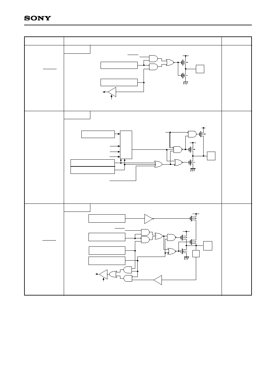
I/O Circuit Format for Pins
Port A
Pin
Circuit format
Pull-up transistors
approx. 100k
Pull-up resistor
Port B data
Port B direction
"0" when reset
RD (Port B)
Data bus
IP
"0" when reset
Schmitt input
SCK in
Output enable
Port B output
selection
"0" when reset
SCK OUT
≠ 9 ≠
CXP83408/83412/83416, CXP83409/83413/83417
2 pins
Hi-Z
Hi-Z
Pin
When reset
Circuit format
PB4/SO0
PB7/SO1
PC0 to PC7
8 pins
5 pins
Hi-Z
PE0/INT0/EC
PE1/INT1
PE2/INT2
PE3/INT3/NMI
PE4/RMC
IP
Schmitt input
INT0/EC
INT1
INT2
INT3/NMI
RMC
Data bus
RD (Port E)
IP
Pull-up resistor
Port C data
Port C direction
"0" when reset
RD (Port C)
Data bus
1
Large current 12mA
2
Pull-up transistors
approx. 100k
2
"0" when reset
1
Pull-up transistors
approx. 100k
Pull-up resistor
Port B data
Port B direction
"0" when reset
RD (Port B)
Data bus
IP
"0" when reset
Output enable
Port B output
selection
"0" when reset
SO
Port E
Port C
Port B
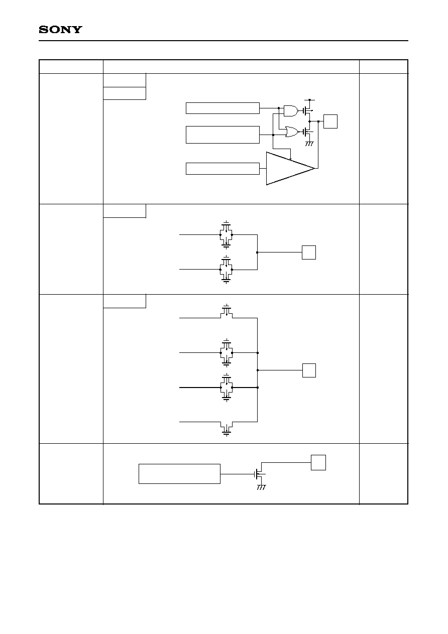
≠ 10 ≠
CXP83408/83412/83416, CXP83409/83413/83417
1 pin
High level
with pull-up
transistor ON
resistor when
reset
High level
Pin
When reset
Circuit format
PE6/TO/ADJ
PE5/PWM0
1
2
Port E data
"1" when reset
Port E output selection (upper)
MPX
Port E output selection (lower)
ADJ2K
ADJ16K
TO
Internal reset signal
1
Pull-up transistors approx. 150k
.
ADJ signals are frequency divider outputs
for 32kHz oscillation frequency adjustment.
ADJ2K provides usage as buzzer output.
2
TO Output enable
Port E
1 pin
Hi-Z
PH0/PWM1
Data bus
RD (Port H)
IP
Port H data
Port H direction
"0" when reset
Pull-up transistors
approx. 100k
Pull-up resistor
Port H output selection
PWM1
"0" when reset
"0" when reset
Port H
1 pin
Port E
Port E output selection
RD (Port E)
Data bus
"0" when reset
Port E data
"1" when reset
PWM0
(
)
≠ 11 ≠
CXP83408/83412/83416, CXP83409/83413/83417
16 pins
V
DD
level
Pin
When reset
Circuit format
SEG0 to SEG15
V
CH
V
CL
Segment
output
(V
DD
level)
PD0 to PD7
PF0 to PF7
Segment data
Segment
driver
Port/segment output
selection
"0" when reset
Port data
PD7 to PD4
PD3 to PD0
PF7 to PF0
by a bit unit
by 4-bit unit
Port D
Port F
4 pins
V
DD
level
COM0 to COM3
V
LC1
V
LC2
V
LC3
V
DD
Common
24 pins
Segment
1 pin
Hi-Z
V
L
LCD control
(DSP bit)
"0" when reset
≠ 12 ≠
CXP83408/83412/83416, CXP83409/83413/83417
2 pins
Oscillation
Pin
When reset
Circuit format
EXTAL
XTAL
EXTAL
XTAL
IP
IP
2 pins
Oscillation
TEX
TX
TEX
TX
IP
IP
1 pin
Low level
RST
IP
Schmitt input
Mask option
Pull-up resistor
OP
∑ Diagram shows circuit
composition during oscillation.
∑ Feedback resistor is removed
during stop, and XTAL
becomes "High" level.
∑ Diagram shows circuit
composition during oscillation.
∑ When the operation of the oscillation circuit is
stopped by the software, the feedback
resistor is removed and TEX and TX become
"Low" level and "High" level respectively.
≠ 13 ≠
CXP83408/83412/83416, CXP83409/83413/83417
1
V
IN
and V
OUT
must not exceed V
DD
+ 0.3V.
2
The large current drive transistor is the N-ch transistor of Port C (PC).
Note) Usage exceeding absolute maximum ratings may permanently impair the LSI. Normal operation should
be conducted under the recommended operating conditions. Exceeding these conditions may adversely
affect the reliability of the LSI.
Supply voltage
LCD bias voltage
Input voltage
Output voltage
High level output current
High level total output current
Low level total output current
Operating temperature
Storage temperature
Allowable power dissipation
V
DD
V
LC1
, V
LC2
,
V
LC3
V
IN
V
OUT
I
OH
I
OH
I
OL
I
OLC
I
OL
Topr
Tstg
P
D
Low level output current
≠0.3 to +7.0
≠0.3 to +7.0
1
≠0.3 to +7.0
1
≠0.3 to +7.0
1
≠5
≠50
15
20
100
≠20 to +75
≠55 to +150
600
380
380
V
V
V
V
mA
mA
mA
mA
mA
∞C
∞C
mW
mW
mW
Output (value per pin)
Total for all output pins
All pins excluding large current output
(value per pin)
Large current outputs (value per pin
2
)
Total for all output pins
QFP-80P-L01
LQFP-80P-L01
QFP-80P-L03
Item
Symbol
Rating
Unit
Remarks
Absolute Maximum Ratings
(Vss = 0V reference)
≠ 14 ≠
CXP83408/83412/83416, CXP83409/83413/83417
1
Value for each pin of normal input ports (PA, PB4, PB7, PC and PH0).
2
Value of the following pins: RST, CS0, CS1, SI0, SI1, SCK0, SCK1, EC/INT0, INT1, INT2, NMI/INT3, and RMC.
3
Specifies only during external clock input.
4
Optimal values are determined by LCD used.
High level input voltage
Low level input voltage
Operating temperature
Supply voltage
LCD bias voltage
5.5
5.5
5.5
5.5
V
DD
V
DD
V
DD
V
DD
+ 0.3
0.3V
DD
0.2V
DD
0.4
+75
V
V
V
V
V
V
V
∞C
V
Item
Symbol
Min.
Max.
Unit
Remarks
4.5
3.5
2.7
2.5
Vss
0.7V
DD
0.8V
DD
V
DD
≠ 0.4
0
0
≠0.3
≠20
V
LC1
V
LC2
V
LC3
V
IH
V
IHS
V
IHEX
V
IL
V
ILS
V
ILEX
Topr
During 1/2 and 1/4 frequency division
operating modes guaranteed operation range
During 1/16 frequency division operating mode
or sleep mode quaranteed operation range
Guaranteed operation range with TEX clock
Guaranteed data hold range during STOP
LCD power supply range
4
1
Hysteresis input
2
EXTAL
3
1
Hysteresis input
2
EXTAL
3
V
DD
Recommended Operating Conditions
(Vss = 0V reference)
≠ 15 ≠
CXP83408/83412/83416, CXP83409/83413/83417
V
DD
= 4.5V, I
OH
= ≠0.5mA
V
DD
= 4.5V, I
OH
= ≠1.2mA
V
DD
= 4.5V, I
OL
= 1.8mA
V
DD
= 4.5V, I
OL
= 3.6mA
V
DD
= 4.5V, I
OL
= 12.0mA
V
DD
= 5.5V, V
IH
= 5.5V
V
DD
= 5.5V, V
IL
= 0.4V
V
DD
= 5.5V, V
IH
= 5.5V
High level
output current
4.0
3.5
0.5
≠0.5
0.1
≠0.1
≠1.5
≠2.78
V
V
V
V
V
V
µA
µA
µA
mA
µA
µA
µA
k
k
PC
PA, PB,
PC, PD
1
,
PE5, PE6,
PF, PH0,
V
L
(Vo
L
only)
EXTAL
TEX
RST
2
Item
Symbol
Pins
Conditions
Min.
V
DD
I
DD1
I
IL
I
IH
I
IZ
I
DD2
I
DDS1
I
DDS2
I
DDS3
V
OH
V
OL
I
IHE
I
ILE
I
IHT
I
ILT
I
ILR
Low level
output current
Input current
3
5
Typ.
0.4
0.6
1.5
40
≠40
10
≠10
≠400
≠45
±10
5
15
Max.
Unit
DC Characteristics
Electrical Characteristics
(Ta = ≠20 to +75∞C, Vss = 0V reference)
V
DD
= 5.5V, 10MHz crystal oscillation
(C
1
= C
2
= 15pF)
V
DD
= 3V, 32kHz crystal oscillation
(C
1
= C
2
= 47pF)
V
DD
= 5.5V, 10MHz crystal oscillation
(C
1
= C
2
= 15pF)
V
DD
= 3V, 32kHz crystal oscillation
(C
1
= C
2
= 47pF)
V
DD
= 5.5V termination of 10MHz
and 32kHz crystal oscillation
Supply
current
4
V
DD
= 5.5V,
V
IL
= 0.4V
V
DD
= 4.5V, V
IH
= 4.0V
V
DD
= 5.5V,
V
I
= 0, 5.5V
V
DD
= 5V,
V
LC1
= 3.75V
V
LC2
= 2.5V
V
LC3
= 1.25V
High-speed mode operation
(1/2 frequency divider clock)
SLEEP mode
STOP mode
I/O leakage
current
R
COM
Common
output
impedance
R
SEG
Segment
output
impedance
PA to PC
3
,
PH
3
,
PE0 to PE4,
RST
2
COM0
to
COM3
SEG0 to SEG15
,
SEG16 to
SEG31
1
40
100
8
10
30
18
35
1.1
9
mA
µA
mA
µA
µA
≠ 16 ≠
CXP83408/83412/83416, CXP83409/83413/83417
Item
Symbol
Pins
Conditions
Min.
PA to PC,
PE1 to PE4,
EXTAL, TEX,
RST
Clock 1MHz
0V for all pins excluding
measured pins
C
IN
Typ.
Max.
Unit
1
Common pins of PD0/SEG16 to PD7/SEG23, PF0/SEG24, PF7/SEG31, PD and PF are the case when the
common pin is selected as port; SEG16 to SEG31 is when the common pin is selected as segment output.
2
RST specifies the input current when pull-up resistor has been selected; leakage current when no resistor
has been selected.
3
PA to PC, and PH0 specify the input current when pull-up resistor has been selected; leakage current when
no resistor has been selected. (PE0 to PE4 specify the leakage current.)
4
When all output pins are left open.
Input capacity
pF
20
10
≠ 17 ≠
CXP83408/83412/83416, CXP83409/83413/83417
1
t
sys indicates the three values below according to the upper two bits (CPU clock selection) of the clock
control registor (CLC: 00FE
H
).
t
sys (ns) = 2000/fc (upper two bits = "00"), 4000/fc (upper two bits = "01"), 16000/fc (upper two bits = "11")
EXTAL
t
XH
t
XL
t
CF
t
CR
0.4V
V
DD
≠ 0.4V
1/fc
Crystal oscillation
Ceramic oscillation
EXTAL
XTAL
External clock
EXTAL
XTAL
74HC04
C
1
C
2
32kHz clock applied condition
Crystal oscillation
TEX
TX
C
1
C
2
AC Characteristics
(1) Clock timing
System clock frequency
System clock input
pulse width
System clock input
rise and fall time
Event count input clock
pulse width
Event count input clock
rise and fall time
System clock frequency
Event count input clock
input pulse width
Event count input clock
rise and fall time
f
C
t
XL
,
t
XH
t
CR
,
t
CF
t
EH
,
t
EL
t
ER
,
t
EF
f
C
t
TL
,
t
TH
t
TR
,
t
TF
XTAL
EXTAL
EXTAL
EXTAL
EC
EC
TEX
TX
TEX
TEX
MHz
ns
ns
ns
ms
kHz
µs
ms
Item
Symbol
Pin
Conditions
Min.
Unit
Fig. 1, Fig. 2
Fig. 1, Fig. 2
External clock drive
Fig. 1, Fig. 2
External clock drive
Fig. 3
Fig. 3
V
DD
= 2.7 to 5.5V
Fig. 2 (32kHz clock
applied condition)
Fig. 3
Fig. 3
1
37.5
t
sys + 50
1
10
Typ.
32.768
Max.
10
200
20
20
(Ta = ≠20 to +75∞C, V
DD
= 4.5 to 5.5V, Vss = 0V reference)
Fig. 2. Clock applied conditions
Fig. 1. Clock timing
TEX
EC
t
EH
t
EL
t
EF
t
ER
0.2V
DD
0.8V
DD
t
TH
t
TL
t
TF
t
TR
Fig. 3. Event count clock timing
≠ 18 ≠
CXP83408/83412/83416, CXP83409/83413/83417
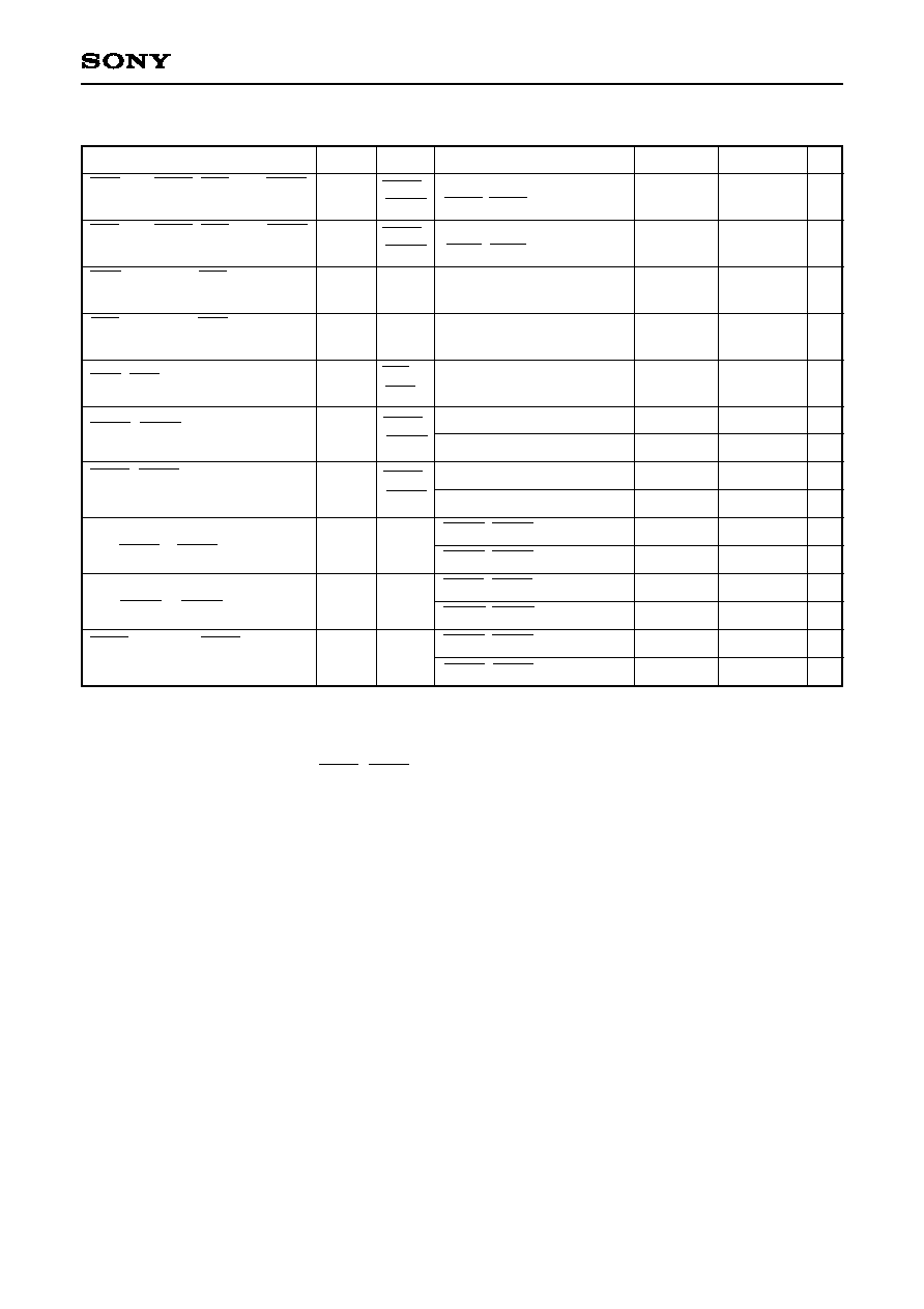
(2) Serial transfer
(Ta = ≠20 to +75∞C, V
DD
= 4.5 to 5.5V, Vss = 0V reference)
Item
CS0
SCK0 (CS1
SCK1)
delay time
CS0
SCK0 (CS1
SCK1)
floating delay time
CS0
SO0 (CS1
SO1)
delay time
CS0
SO0 (CS1
SO1)
floating delay time
CS0 (CS1) high level width
SCK0 (SCK1) cycle time
SCK0 (SCK1)
high and low level widths
SI0 (SI1) input setup time
(for SCK0
(SCK1
) )
SI0 (SI1) input hold time
(for SCK0
(SCK1
) )
SCK0
SO0 (SCK1
SO1)
delay time
t
DCSK
t
DCSKF
t
DCSO
t
DCSOF
t
WHCS
t
KCY
t
KH
t
KL
t
SIK
t
KSI
t
KSO
SCK0
(SCK1)
SCK0
(SCK1)
SO0
(SO1)
SO0
(SO1)
CS0
(CS1)
SCK0
(SCK1)
SCK0
(SCK1)
SI0
(SI1)
SI0
(SI1)
SO0
(SO1)
Input mode
Output mode
Input mode
Output mode
SCK0 (SCK1) input mode
SCK0 (SCK1) output mode
SCK0 (SCK1) input mode
SCK0 (SCK1) output mode
SCK0 (SCK1) input mode
SCK0 (SCK1) output mode
ns
ns
ns
ns
ns
Symbol
Pin
Min.
t
sys + 200
t
sys + 200
t
sys + 200
t
sys + 200
t
sys + 200
2
t
sys + 200
16000/fc
t
sys + 100
8000/fc ≠ 50
100
200
t
sys + 200
100
ns
ns
ns
ns
ns
ns
ns
ns
ns
ns
t
sys + 200
100
Max.
Unit
Chip select transfer mode
(SCK0 (SCK1) = output mode)
Chip select transfer mode
(SCK0 (SCK1) = output mode)
Chip select transfer mode
Chip select transfer mode
Chip select transfer mode
Conditions
Note 1)
t
sys indicates the three values below according to the upper two bits (CPU clock selection) of the
clock control register (CLC: 00FE
H
).
t
sys (ns) = 2000/fc (upper two bits = "00"), 4000/fc (upper two bits = "01"), 16000/fc (upper two bits = "11")
Note 2) The load condition for the SCK0 (SCK1) output mode, SO0 (SO1) output delay time is 50pF + 1TTL.
≠ 19 ≠
CXP83408/83412/83416, CXP83409/83413/83417
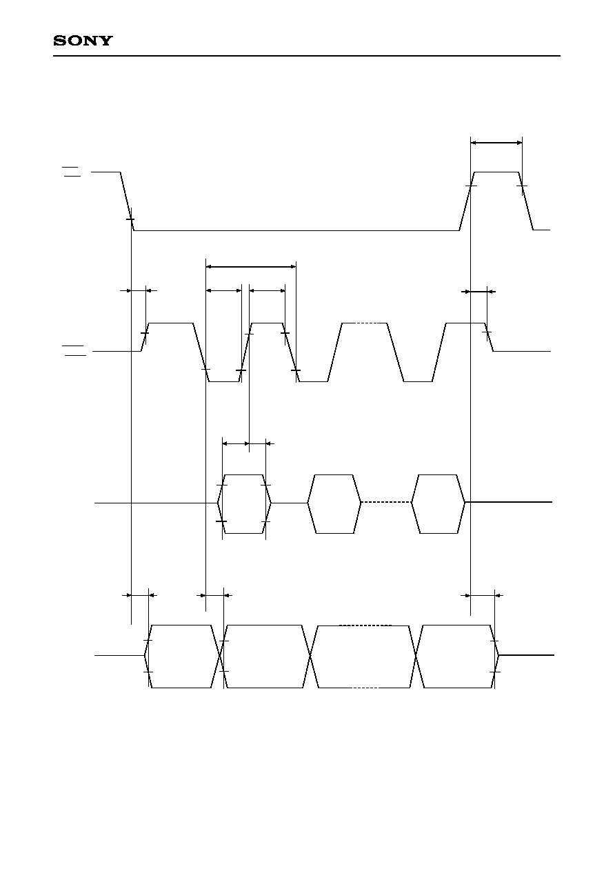
Fig. 4. Serial transfer CH0 timing
CS0
(CS1)
SCK0
(SCK1)
0.2V
DD
0.8V
DD
t
WHCS
t
DCSK
t
DCSKF
0.8V
DD
0.2V
DD
0.8V
DD
t
KCY
t
KL
t
KH
0.8V
DD
0.2V
DD
SI0
(SI1)
t
SIK
t
KSI
Input
data
t
DCSO
t
KSO
t
DCSOF
Output data
0.8V
DD
0.2V
DD
SO0
(SO1)
≠ 20 ≠
CXP83408/83412/83416, CXP83409/83413/83417
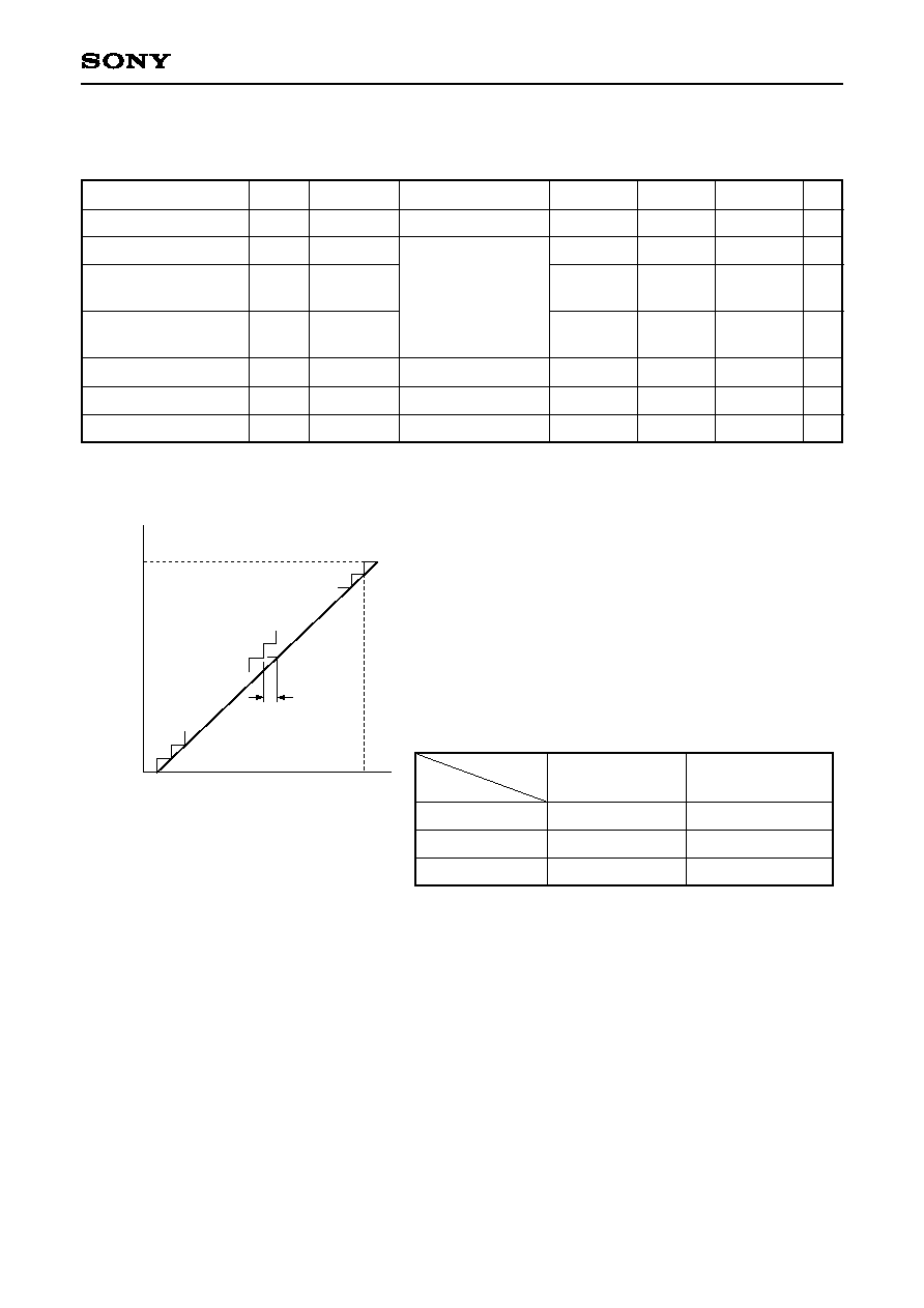
Conversion time
Sampling time
Analog input voltage
t
CONV
t
SAMP
V
IAN
V
ZT
1
V
FT
2
AN0 to AN7
Ta = 25∞C
V
DD
= 5.0V
V
SS
= 0V
Linearity error
Zero transition voltage
Full-scale transition
voltage
Resolution
µs
µs
V
V
DD
+ 0.3
160/f
ADC
3
12/f
ADC
3
0
Item
Symbol
Pin
Conditions
Min.
Typ.
Max.
Unit
Bits
(3) A/D converter characteristics
(Ta = ≠20 to +75∞C, V
DD
= 4.5 to 5.5V, AV
REF
= 4.0 to AV
DD
, Vss = 0V reference)
8
±3
LSB
70
mV
5030
10
4970
≠10
4910
mV
Fig. 5. Definition of A/D converter terms
Analog input
Linearity error
V
FT
V
ZT
00
H
01
H
FE
H
FF
H
Digital conversion value
00 (
= f
EX
/2)
01 (
= f
EX
/4)
11 (
= f
EX
/16)
f
ADC
= fc/2
f
ADC
= fc/4
f
ADC
= fc/16
f
ADC
= fc
f
ADC
= fc/2
f
ADC
= fc/8
CKS
PCK1, PCK0
0 (
/2 selection)
0 (
selection)
1
V
ZT
: Value atwhich the digital conversion value changes
from 00
H
to 01
H
and vice versa.
2
V
FT
: Value at which the digital conversion value changes
from FE
H
to FF
H
and vice versa.
3
f
ADC
indicates the below values due to the contents of bit 6
(CK3) of the A/D control registor (ADC: 00F9
H
) and bit 7
(PCK1) and bit 6 (PCK0) of the clock control resistor (CLC:
00FE
H
).
≠ 21 ≠
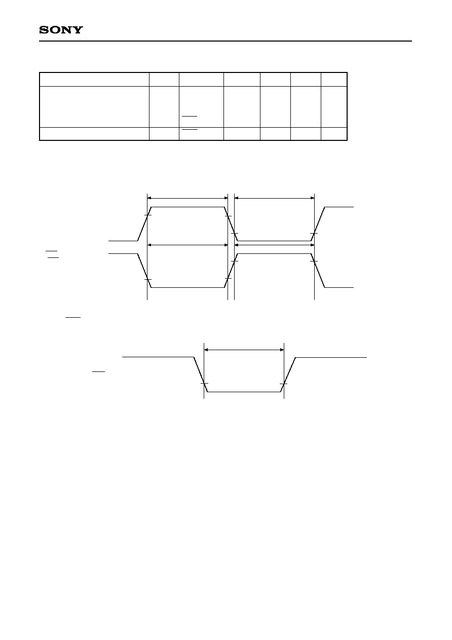
CXP83408/83412/83416, CXP83409/83413/83417
External interruption
high and low level widths
Reset input low level width
INT0
INT1
INT2
NMI/INT3
RST
1
32/fc
µs
µs
Item
Symbol
Pin
Conditions
Min.
Max.
Unit
t
IH
t
IL
t
RSL
(4) Interruption, reset input
(Ta = ≠20 to +75∞C, V
DD
= 4.5 to 5.5V, Vss = 0V reference)
0.2V
DD
0.8V
DD
t
IH
t
IL
t
IL
t
IH
INT0
INT1
INT2
NMI/INT3
(NMI is specified only for
the falling edge)
Fig 6. Interruption input timing
t
RSL
0.2V
DD
RST
Fig. 7. RST input timing
≠ 22 ≠
CXP83408/83412/83416, CXP83409/83413/83417
Appendix
Fig. 8. SPC700 Series recommended oscillation circuit
C
1
EXTAL
XTAL
C
2
Rd
EXTAL
XTAL
Rd
(i) Main clock
EXTAL
XTAL
C
1
C
2
Rd
XTAL
(ii) Main clock
EXTAL
XTAL
C
1
C
2
Rd
TEX
TX
(iii) Sub clock
Manufacturer
MURATA
MFG
CO., LTD.
RIVER
ELETEC
CO., LTD.
KINSEKI
LTD.
Model
CSA4.19MG
CSA8.00MG
CST4.19MGW
1
CST8.00MTW
1
HC-49/U03
HC-49/U (-S)
fc (MHz)
4.19
8.00
10.00
4.19
8.00
10.00
4.19
8.00
10.00
4.19
8.00
10.00
18
18
30
15
22
30
15
22
0
2.2k
470
560
0
C
1
(pF)
C
2
(pF)
Rd (
)
Circuit
example
(i)
CSA10.0MT
(ii)
CST10.00MTW
1
(i)
Models with an asterisk (
1
) have the built-in ground capacitance (C
1
, C
2
).
Item
Content
Reset pin pull-up resistor
Non-existent
Existent
Mask Option Table
Product name
Package
CXP83408/83412/83416
CXP83409/83413/83417
80-pin plastic QFP/LQFP
80-pin plastic QFP (0.65mm pitch)
Package Table
≠ 23 ≠
CXP83408/83412/83416, CXP83409/83413/83417
(100µA)
3
4
5
6
0.1
5.0
1.0
V
DD
≠ Supply voltage [V]
I
DD
≠ Supply current [mA]
I
DD
vs. V
DD
(fc = 10MHz, Ta = 25∞C, Typical)
7
2
0.05
(50µA)
0.01
(10µA)
0.5
10.0
20.0
SLEEP mode
32kHz mode
(instruction)
32kHz
SLEEP mode
SLEEP mode
0
15
10
5
fc ≠ System clock [MHz]
I
DD
≠ Supply current [mA]
I
DD
vs. fc
5
10
16
20
1/2 dividing mode
1/2 dividing mode
(V
DD
= 5V, Ta = 25∞C, typical)
Characteristic Curves
Package Outline
Unit : mm
CXP83408/83412/83416
PACKAGE STRUCTURE
SONY CODE
EIAJ CODE
JEDEC CODE
QFP-80P-L01
QFP080-P-1420-A
PACKAGE MATERIAL
LEAD TREATMENT
LEAD MATERIAL
PACKAGE WEIGHT
EPOXY RESIN
SOLDER PLATING
COPPER / 42 ALLOY
1.6g
23.9 ± 0.4
20.0 ≠ 0.1
+ 0.4
1
80
65
64
41
40
25
24
0.8
0.35 ≠ 0.1
+ 0.15
14.0 ≠ 0.1
+ 0.4
17.9 ±
0.4
16.3
0.1 ≠ 0.05
+ 0.2
2.75 ≠ 0.15
+ 0.35
0.8 ±
0.2
0.15 ≠ 0.05
+ 0.1
80PIN QFP (PLASTIC)
M
0.12
0.15
0∞ to 10∞
DETAIL A
A
≠ 24 ≠
CXP83408/83412/83416, CXP83409/83413/83417
CXP83409/83413/83417
SONY CODE
EIAJ CODE
JEDEC CODE
PACKAGE MATERIAL
LEAD TREATMENT
LEAD MATERIAL
PACKAGE WEIGHT
EPOXY / PHENOL RESIN
SOLDER PLATING
42 ALLOY
PACKAGE STRUCTURE
14.0 ± 0.2
12.0 ± 0.1
(0.22)
60
41
40
21
20
80
61
1
0.5 ± 0.08
0.18 ≠ 0.03
+ 0.08
A
1.5 ≠ 0.1
+ 0.2
0.127 ≠ 0.02
+ 0.05
0.5 ±
0.2
(13.0)
0.1 ± 0.1
0.5 ±
0.2
0∞ to 10∞
DETAIL A
80PIN LQFP (PLASTIC)
0.5g
LQFP-80P-L01
QFP080-P-1212-A
0.1
NOTE: Dimension "
" does not include mold protrusion.
SONY CODE
EIAJ CODE
JEDEC CODE
PACKAGE STRUCTURE
PACKAGE MATERIAL
LEAD TREATMENT
LEAD MATERIAL
PACKAGE WEIGHT
EPOXY RESIN
SOLDER PLATING
COPPER / 42 ALLOY
QFP-80P-L03
LQFP080-P-1414
0.6g
80PIN QFP (PLASTIC)
16.0 ± 0.4
14.0 ≠ 0.1
+ 0.4
0.65
0.3 ≠ 0.1
+ 0.15
0∞ to 10∞
0.5 ±
0.2
0.1 ≠ 0.1
+ 0.15
(15.0)
0.127 ≠ 0.05
+ 0.1
1.5 ≠ 0.15
+ 0.35
40
21
20
1
41
60
61
80
M
± 0.12
0.1
CXP83408/83412/83416