≠ 1 ≠
E98342C1Y-PS
Sony reserves the right to change products and specifications without prior notice. This information does not convey any license by
any implication or otherwise under any patents or other right. Application circuits shown, if any, are typical examples illustrating the
operation of the devices. Sony cannot assume responsibility for any problems arising out of the use of these circuits.
CXP836P60
CXP836P61
CMOS 8-bit Single Chip Microcomputer
Description
The CXP836P60/836P61 is a CMOS 8-bit single
chip microcomputer integrating on a single chip an
A/D converter, serial interface, timer/counter, time-
base timer, sub timer/counter, LCD controller/driver
and remote control reception circuit besides the basic
configurations of 8-bit CPU, PROM, RAM, and I/O
port.
The CXP836P60/836P61 also provides a sleep/stop
function that enables lower power consumption.
The CXP836P60 and CXP836P61 are the PROM-
incorporated version of the CXP83508/83512/83516/
83620/83624 and CXP83509/83513/83517/83621/83625
with built-in mask ROM, and they are able to write
directly into the program. Thus, it is most suitable for
evaluation use during system development and for
small-quantity production.
Features
∑ Wide-range instruction system (213 instructions) to
cover various types of data.
-- 16-bit arithmetic/multiplication and division/boolean bit operation instructions
∑ Minimum instruction cycle
400ns at 10MHz operation (4.5 to 5.5V)
1µs at 4MHz operation (2.7 to 5.5V)
122µs at 32kHz operation (2.7 to 5.5V)
∑ Incorporated PROM capacity 60K bytes
∑ Incorporated RAM capacity
736 bytes (includes LCD display data area and serial interface RAM)
∑ Peripheral functions
-- A/D converter
8-bit, 8-channel, successive approximation method
(Conversion time of 12.4µs/10MHz)
-- Serial interface
Incorporated buffer RAM
(Auto transfer for 1 to 32 bytes), 1 channel
8-bit clock synchronized type (MSB/LSB first selectable), 1 channel
-- Timer
8-bit timer, 8-bit timer/counter, 19-bit time-base timer,
Sub timer/counter
-- LCD controller/driver
Maximum 128 segment display possible (during 1/4 duty)
4 common output, 32 segment output
Display method static, 1/2, 1/3, 1/4 duty
Bias method 1/2, 1/3 bias
-- Remote control reception circuit
8-bit pulse measuring counter, 6-stage FIFO
∑ Interruption
14 factors, 14 vectors, multi-interruption possible
∑ Standby mode
Sleep/stop
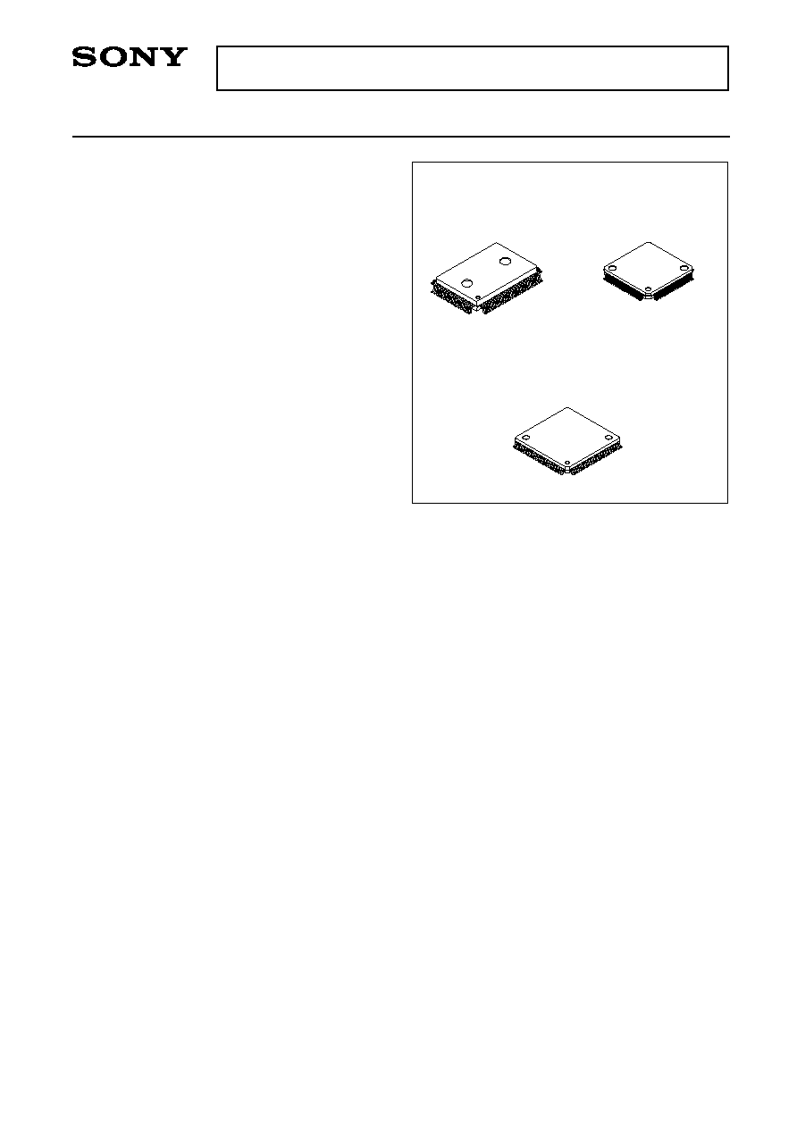
∑ Package
80-pin plastic QFP/LQFP
Structure
Silicon gate CMOS IC
CXP836P60
80 pin QFP (Plastic) 80 pin LQFP (Plastic)
CXP836P61
80 pin QFP (Plastic)
≠ 2 ≠
CXP836P60, CXP836P61
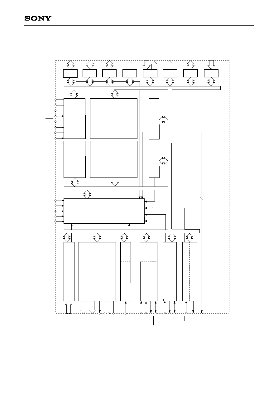
XTAL
A/D CONVERTER
REMOCON
SERIAL
INTERFACE
UNIT (CH0)
8-BIT TIMER/COUNTER 0
8-BIT TIMER 1
FIFO
BUFFER
RAM
INTERRUPT CONTROLLER
SPC700
CPU CORE
PROM
60K BYTES
PRESCALER/
TIME-BASE TIMER
SUB TIMER/
COUNTER
RAM
736 BYTES
8
AN0 to AN7
RMC
SI0
SO0
SI1
SO1
EC
CS0
SCK0
SCK1
INT0
INT1
INT2
INT3
TEX
TX
EXTAL
V
DD
Vss
PORT C
8
PC0 to PC7
PORT H
1
PH0
PORT B
8
PB0 to PB7
PORT E
5
2
PE0 to PE4
PE5 to PE6
2
LCD
CONTROLLER/DRIVER
32
SEG0 to SEG31
4
COM0 to COM3
V
L
V
LC1
V
LC2
PORT A
8
PA0 to PA7
PORT D
8
PD0 to PD7
PORT F
8
PF0 to PF7
V
LC3
ADJ
TO
CLOCK GENERATOR/
SYSTEM CONTROL
RST
3
INT4
PORT I
2
PI0 to PI1
SERIAL INTERFACE UNIT
(CH1)
Vpp
Block Diagram
≠ 3 ≠
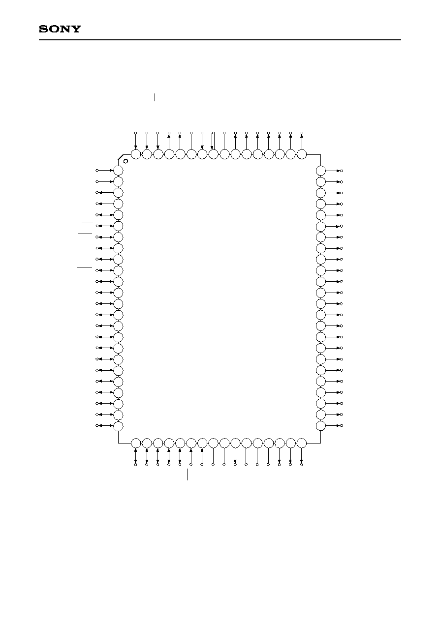
CXP836P60, CXP836P61
Pin Assignment (Top View) CXP836P60 (QFP package)
PE3/INT3
PE4/RMC
PE5/TO
PE6/ADJ
PB0
PB1/CS0
PB2/SCK0
PB3/SI0
PB4/SO0
PB5/SCK1
PB6/SI1
PB7/SO1
PC0
PC1
PC2
PC3
PC4
PC5
PC6
PC7
PH0/INT4
PA0/AN0
PA1/AN1
PA2/AN2
PD6/SEG22
PD5/SEG21
PD4/SEG20
PD3/SEG19
PD2/SEG18
PD1/SEG17
PD0/SEG16
SEG15
SEG14
SEG13
SEG12
SEG11
SEG10
SEG9
SEG8
SEG7
SEG6
SEG5
SEG4
SEG3
SEG2
SEG1
SEG0
COM3
PA3/AN3
PA4/AN4
PA5/AN5
PA6/AN6
PA7/AN7
RST
EXTAL
XTAL
V
SS
V
L
V
LC3
V
LC2
V
LC1
COM0
COM1
COM2
PE2/INT2
PE1/INT1
PE0/INT0/EC
PF7/SEG31
PF6/SEG30
Vpp
PI1/TEX
PI0/TX
V
DD
PF5/SEG29
PF4/SEG28
PF3/SEG27
PF2/SEG26
PF1/SEG25
PF0/SEG24
PD7/SEG23
2
3
4
5
6
7
8
9
10
11
12
13
14
15
16
17
18
19
20
21
22
23
24
25 26 27 28 29 30
40
39
38
37
36
35
34
31 32 33
70 69 68 67
65
66
71
72
73
74
75
76
77
78
79
80
1
41
42
43
44
45
46
47
48
49
50
51
52
53
54
55
56
57
58
59
60
63
64
61
62
Note) Do not make any connections to Vpp (Pin 75).

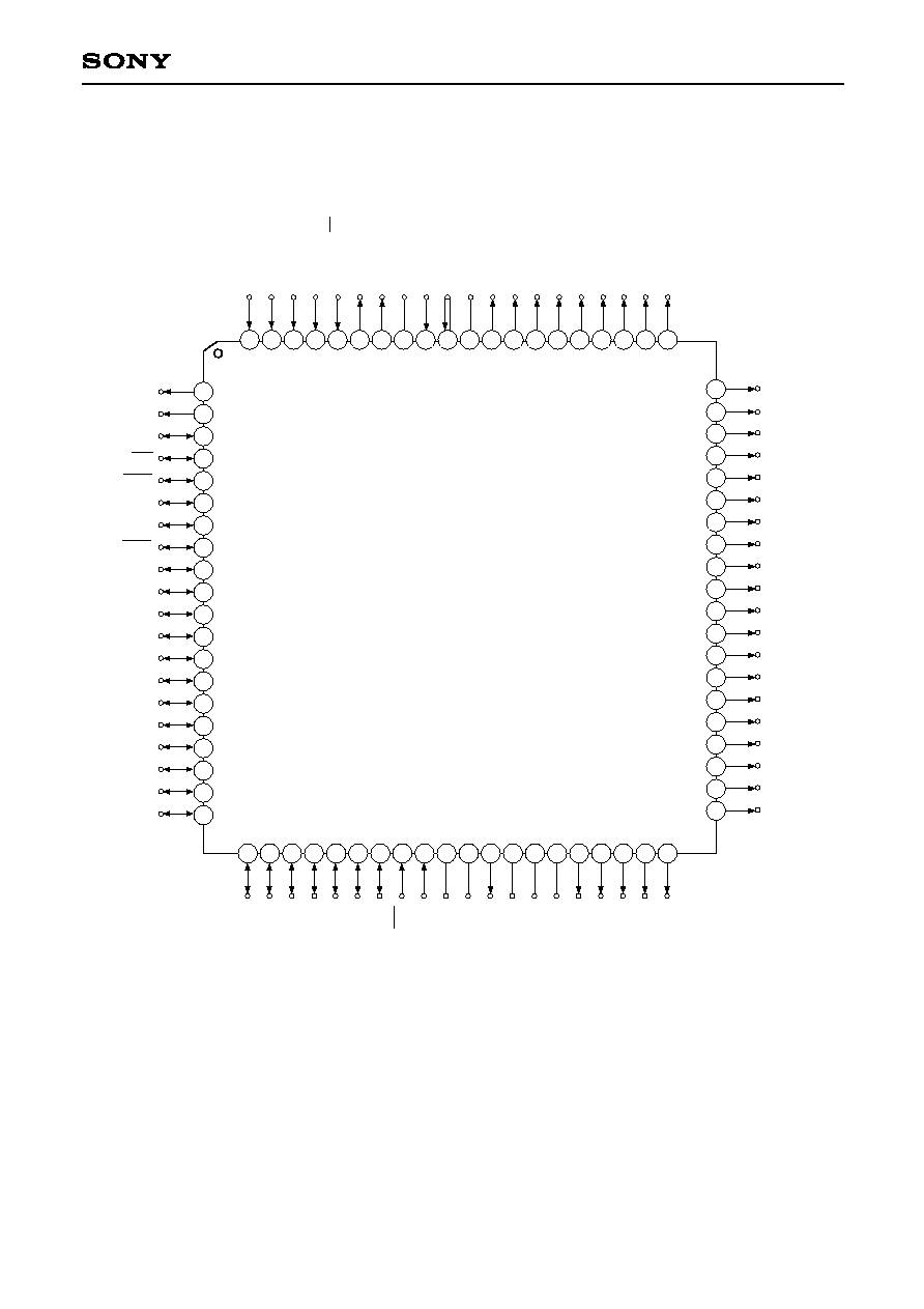
≠ 4 ≠
CXP836P60, CXP836P61
Pin Assignment (Top View) CXP836P60 (LQFP package)
PE5/TO
PE6/ADJ
PB0
PB1/CS0
PB2/SCK0
PB3/SI0
PB4/SO0
PB5/SCK1
PB6/SI1
PB7/SO1
PC0
PC1
PC2
PC3
PC4
PC5
PC6
PC7
PH0/INT4
PA0/AN0
PD4/SEG20
PD3/SEG19
PD2/SEG18
PD1/SEG17
PD0/SEG16
SEG15
SEG14
SEG13
SEG12
SEG11
SEG10
SEG9
SEG8
SEG7
SEG6
SEG5
SEG4
SEG3
SEG2
SEG1
PA1/AN1
PA2/AN2
PA3/AN3
PA4/AN4
PA5/AN5
PA6/AN6
PA7/AN7
RST
EXTAL
XTAL
V
SS
V
L
V
LC3
V
LC2
V
LC1
COM0
COM1
COM2
COM3
SEG0
PE4/RMC
PE3/INT3
PE2/INT2
PE1/INT1
PE0/INT0/EC
PF7/SEG31
PF6/SEG30
Vpp
PI1/TEX
PI0/TX
V
DD
PF5/SEG29
PF4/SEG28
PF3/SEG27
PF2/SEG26
PF1/SEG25
PF0/SEG24
PD7/SEG23
PD6/SEG22
PD5/SEG21
2
3
4
5
6
7
8
9
10
11
12
13
14
15
16
17
18
19
20
21 22 23 24 25 26 27 28 29 30
40
39
38
37
36
35
34
31 32 33
70 69 68 67
65
66
71
72
73
74
75
76
77
78
79
80
1
41
42
43
44
45
46
47
48
49
50
51
52
53
54
55
56
57
58
59
60
63
64
61
62
Note) Do not make any connections to Vpp (Pin 73).
≠ 5 ≠
CXP836P60, CXP836P61
Pin Assignment (Top View) CXP836P61 (QFP package)
PE5/TO
PE6/ADJ
PB0
PB1/CS0
PB2/SCK0
PB3/SI0
PB4/SO0
PB5/SCK1
PB6/SI1
PB7/SO1
PC0
PC1
PC2
PC3
PC4
PC5
PC6
PC7
PH0/INT4
PA0/AN0
PD4/SEG20
PD3/SEG19
PD2/SEG18
PD1/SEG17
PD0/SEG16
SEG15
SEG14
SEG13
SEG12
SEG11
SEG10
SEG9
SEG8
SEG7
SEG6
SEG5
SEG4
SEG3
SEG2
SEG1
PA1/AN1
PA2/AN2
PA3/AN3
PA4/AN4
PA5/AN5
PA6/AN6
PA7/AN7
RST
EXTAL
XTAL
V
SS
V
L
V
LC3
V
LC2
V
LC1
COM0
COM1
COM2
COM3
SEG0
PE4/RMC
PE3/INT3
PE2/INT2
PE1/INT1
PE0/INT0/EC
PF7/SEG31
PF6/SEG30
Vpp
PI1/TEX
PI0/TX
V
DD
PF5/SEG29
PF4/SEG28
PF3/SEG27
PF2/SEG26
PF1/SEG25
PF0/SEG24
PD7/SEG23
PD6/SEG22
PD5/SEG21
2
3
4
5
6
7
8
9
10
11
12
13
14
15
16
17
18
19
20
21 22 23 24 25 26 27 28 29 30
40
39
38
37
36
35
34
31 32 33
70 69 68 67
65
66
71
72
73
74
75
76
77
78
79
80
1
41
42
43
44
45
46
47
48
49
50
51
52
53
54
55
56
57
58
59
60
63
64
61
62
Note) Do not make any connections to Vpp (Pin 73).
≠ 6 ≠
CXP836P60, CXP836P61
Pin Description
Symbol
I/O
Functions
I/O/Analog input
PA0/AN0
to
PA7/AN7
(Port A)
8-bit I/O port. I/O can
be set in a bit unit.
Standby release input
can be set in a bit unit.
Incorporation of pull-up
resistor can be set
through the program in
a bit unit.
(8 pins)
Analog inputs to A/D converter.
(8 pins)
I/O
PC0 to PC7
PE0/INT0/EC
PE1/INT1
PE2/INT2
PE3/INT3
PE4/RMC
PE5/TO
PE6/ADJ
PH0/INT4
PI0/TX
PI1/TEX
Input/Input/Input
Input/Input
Input/Input
Input/Input
Input/Input
Output/Output
Output/Output
I/O/Input
Input
Input/Input
(Port C)
8-bit I/O port. I/O can be set in a bit unit. Capable of driving 12mA sink
current. Incorporation of pull-up resistor can be set through the program
in a bit unit.
(8 pins)
(Port E)
7-bit port. Lower 5 bits
are for inputs; upper 2
bits are for outputs.
(7 pins)
(Port H)
1-bit I/O port.
Incorporation of pull-up
resistor can be set
through the program.
(1 pin)
(Port I)
2-bit input port.
(2 pins)
External interruption request input.
(1 pin)
Crystal connectors for sub timer/counter clock
oscillation. For usage as event counter, input to
TEX, and leave TX open.
External event inputs for 8-bit timer/counter.
External interruption request inputs.
(4 pins)
Remote control reception circuit input.
Output for 8-bit timer/counter rectangular wave.
Output for TEX oscillation frequency division.
I/O
I/O/Input
I/O/I/O
I/O/Input
I/O/Output
I/O/I/O
I/O/Input
I/O/Output
PB0
PB1/CS0
PB2/SCK0
PB3/SI0
PB4/SO0
PB5/SCK1
PB6/SI1
PB7/SO1
(Port B)
8-bit I/O port. I/O can
be set in a bit unit.
Incorporation of pull-up
resistor can be set
through the program in
a bit unit.
(8 pins)
Chip select input for serial interface (CH0).
Serial clock I/O (CH0).
Serial data input (CH0).
Serial data output (CH0).
Serial clock I/O (CH1).
Serial data input (CH1).
Serial data output (CH1).
≠ 7 ≠
CXP836P60, CXP836P61
Symbol
I/O
Functions
Output/Output
PF0/SEG24
to
PF7/SEG31
(Port F)
8-bit output port.
(8 pins)
Output/Output
PD0/SEG16
to
PD7/SEG23
(Port D)
8-bit output port.
(8 pins)
Output
SEG0 to SEG15
LCD segment signal output. (16 pins)
Input
Crystal connectors for system clock oscillation. When the clock is supplied
externally, input to EXTAL; opposite phase clock should be input to XTAL.
EXTAL
Output
COM0 to COM3
LCD common signal output. (4 pins)
V
LC1
to V
LC3
LCD bias power supply. (3 pins)
Output
V
L
Control pin to cut off the current flowing to external LCD bias resistor
during standby.
XTAL
Input
Low-level active system reset.
Positive power supply pin for writing of built-in PROM.
Do not make any connections under normal operation.
Positive power supply.
GND.
RST
Vpp
V
DD
V
SS
LCD segment signal outputs.
(16 pins)
≠ 8 ≠
CXP836P60, CXP836P61
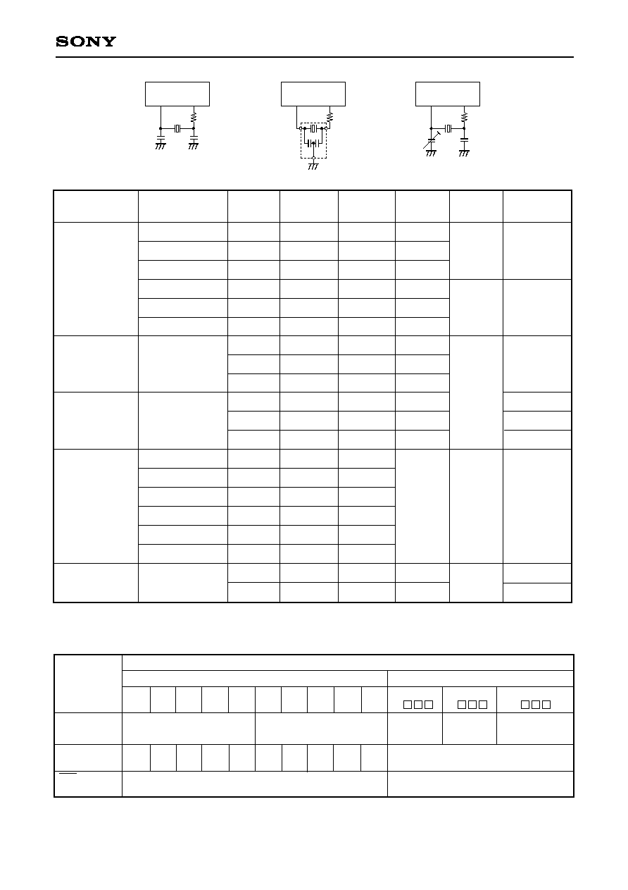
Pull-up transistor
approx. 100k
(V
DD
= 4.5 to 5.5V)
approx. 150k
(V
DD
= 2.7 to 3.3V)
IP
Pull-up resistor
Port B data
Port B direction
"0" after a reset
RD (Port B)
"0" after a reset
Internal data bus
Pull-up transistor
approx. 100k
(V
DD
= 4.5 to 5.5V)
approx. 150k
(V
DD
= 2.7 to 3.3V)
IP
Pull-up resistor
Port B data
Port B direction
"0" after a reset
RD (Port B)
"0" after a reset
Internal data bus
CS0
SI0
SI1
Schmitt input
Port B
8 pins
Hi-Z
Hi-Z
After a reset
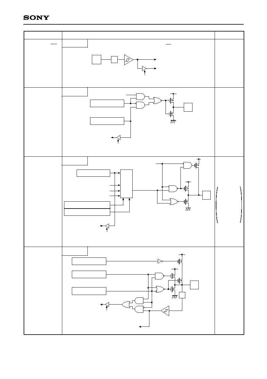
PA0/AN0
to
PA7/AN7
PB0
Port B
1 pin
3 pins
Hi-Z
PB1/CS0
PB3/SI0
PB6/SI1
Pull-up transistor
approx. 100k
(V
DD
= 4.5 to 5.5V)
approx. 150k
(V
DD
= 2.7 to 3.3V)
IP
Pull-up resistor
Port A data
Port A direction
"0" after a reset
Port A function select
"0" after a reset
RD (Port A)
A/D converter
Input multiplexer
"0" after a reset
Input protection
circuit
Edge detection
circuit
Internal data bus
Standby release
I/O Circuit Format for Pins
Port A
Pin
Circuit format
≠ 9 ≠
CXP836P60, CXP836P61
Pull-up resistor
"0" after a reset
RD (Port B)
"0" after a reset
Internal
data bus
Port B data
Port B direction
IP
Serial data output ebable
Port B function select
"0" after a reset
SO
"0" after a reset
Pull-up transistor
approx. 100k
(V
DD
= 4.5 to 5.5V)
approx. 150k
(V
DD
= 2.7 to 3.3V)
Output buffer capability
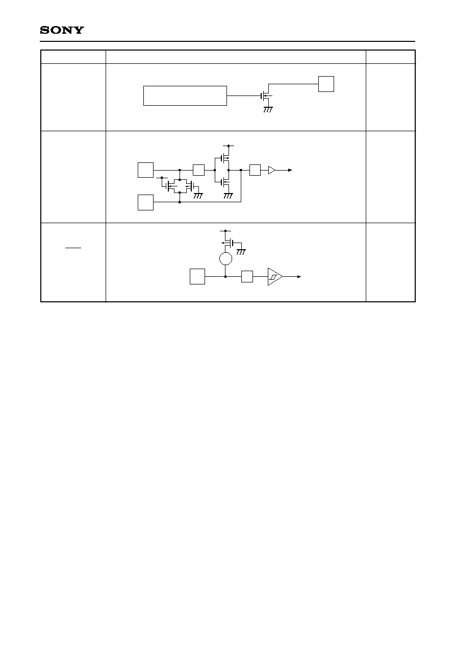
Port B
Port C
2 pins
Hi-Z
Hi-Z
After a reset
PB2/SCK0
PB5/SCK1
PB4/SO0
PB7/SO1
2 pins
Hi-Z
PC0 to PC7
8 pins
Pull-up resistor
"0" after a reset
RD (Port B)
"0" after a reset
Schmitt input
SCK in
Internal
data bus
Port B data
Port B direction
IP
Serial clock output ebable
Port B function select
"0" after a reset
SCK out
"0" after a reset
Pull-up transistor
approx. 100k
(V
DD
= 4.5 to 5.5V)
approx. 150k
(V
DD
= 2.7 to 3.3V)
Output buffer capability
Port B
Pin
Circuit format
IP
Pull-up resistor
Port C data
Port C direction
"0" after a reset
RD (Port C)
"0" after a reset
2
Internal data bus
1
2
Pull-up transistor
approx. 100k
(V
DD
= 4.5 to 5.5V)
approx. 150k
(V
DD
= 2.7 to 3.3V)
1
High current drive
12mA (V
DD
= 4.5 to 5.5V)
4.5mA (V
DD
= 2.7 to 3.3V)
≠ 10 ≠
CXP836P60, CXP836P61
Port E function select
RD (Port E)
Internal data bus
"0" after a reset
Port E data
"1" after a reset
TO
Port E
Port E
Port H
5 pins
Hi-Z
High level
After a reset
PE0/INT0/EC
PE1/INT1
PE2/INT2
PE3/INT3
PE4/RMC
PE5/TO
1 pin
PE6/ADJ
1 pin
Hi-Z
PH0/INT4
1 pin
IP
Schmitt input
INT0/EC
INT1
INT2
INT3
RMC
Internal data bus
RD (Port E)
Port E
Pin
Circuit format
Port E data
"1" after a reset
MPX
ADJ2K
ADJ16K
ADJ32K
Internal reset signal
2
1
ADJ signals are frequency driver
outputs for TEX oscillation frequency
adjustment.
ADJ2K provides usage as buzzer output.
2
Pull-up transistor
approx. 150k
(V
DD
= 4.5 to 5.5V)
approx. 200k
(V
DD
= 2.7 to 3.3V)
1
Port E function select (upper)
Port E function select (lower)
RD (Port E)
Internal data bus
00
"00" after a reset
01
10
11
Pull-up transistor
approx. 100k
(V
DD
= 4.5 to 5.5V)
approx. 150k
(V
DD
= 2.7 to 3.3V)
IP
Pull-up resistor
Port H data
Port H direction
"0" after a reset
RD (Port H)
"0" after a reset
Internal data bus
INT4
Schmitt input
High level
High level
at ON
resistance
of pull-up
transistor
during a
reset.

≠ 11 ≠
CXP836P60, CXP836P61
Segment data
Segment
driver
Port/segment output select
"0" after a reset
Port D, F data
Port D
Port F
Segment
Common
2 pins
Oscillation
halted port
input
Segment
Output
(V
DD
level)
After a reset
PI0/TX
PI1/TEX
PD0/SEG16
to
PD7/SEG23
PF0/SEG24
to
PF7/SEG31
16 pins
V
DD
level
SEG0 to SEG15
16 pins
V
DD
level
COM0 to COM3
4 pins
"1" after a reset
RD (Port I)
Internal data bus
Schmitt input
IP
IP
RD (Port I)
Internal data bus
Clock input
PI1/TEX
PI0/TX
TEX oscillation control circuit
Port I
Pin
Circuit format
V
CH
V
CL
V
LC1
V
LC2
V
LC3
V
DD
≠ 12 ≠
CXP836P60, CXP836P61
EXTAL
XTAL
IP
IP
∑ Diagram shows circuit
composition during
oscillation.
∑ Feedback resistor is
removed during stop.
XTAL becomes high
level.
1 pin
Hi-Z
Oscillation
After a reset
V
L
EXTAL
XTAL
2 pins
Low level
(during a reset)
RST
1 pin
LCD control
(DSP bit)
"0" after a reset
Pin
Circuit format
IP
Schmitt input
Mask option
Pull-up resistor
OP
≠ 13 ≠
CXP836P60, CXP836P61
1
V
IN
and V
OUT
must not exceed V
DD
+ 0.3V.
2
The high current drive transistor is the N-ch transistor of Port C (PC).
Note) Usage exceeding absolute maximum ratings may permanently impair the LSI. Normal operation should
be conducted under the recommended operating conditions. Exceeding these conditions may adversely
affect the reliability of the LSI.
Supply voltage
LCD bias voltage
Input voltage
Output voltage
High level output current
High level total output current
Low level output current
Low level total output current
Operating temperature
Storage temperature
Allowable power dissipation
V
DD
Vpp
V
LC1
, V
LC2
,
V
LC3
V
IN
V
OUT
I
OH
I
OH
I
OL
I
OLC
I
OL
Topr
Tstg
P
D
≠0.3 to +7.0
≠0.3 to +13.0
≠0.3 to +7.0
1
≠0.3 to +7.0
1
≠0.3 to +7.0
1
≠5
≠50
15
20
100
≠20 to +75
≠55 to +150
600
380
380
V
V
V
V
V
mA
mA
mA
mA
mA
∞C
∞C
mW
mW
mW
PROM incorporated version fixed
Output per pin
Total for all output pins
Value per pin, excluding high current
output pins
Value per pin for high current output pins
2
Total for all output pins
QFP-80P-L01
LQFP-80P-L01
QFP-80P-L03
Item
Symbol
Rating
Unit
Remarks
Absolute Maximum Ratings
(Vss = 0V)
≠ 14 ≠
CXP836P60, CXP836P61
Recommended Operating Conditions
(Vss = 0V)
LCD bias voltage
High level
input voltage
Low level
input voltage
Operating temperature
Supply voltage
5.5
5.5
5.5
V
DD
V
DD
V
DD
V
DD
+ 0.3
0.3V
DD
0.2V
DD
0.4
+75
V
V
V
V
V
V
V
∞C
V
Item
Symbol
Min.
Max.
Unit
Remarks
2.7
2.7
2.5
Vss
0.7V
DD
0.8V
DD
V
DD
≠ 0.4
0
0
≠0.3
≠20
V
LC1
V
LC2
V
LC3
V
IH
V
IHS
V
IHEX
V
IL
V
ILS
V
ILEX
Topr
Guaranteed operation range during 1/16
frequency dividing mode or sleep mode
Guaranteed operation range with TEX clock
Guaranteed data hold range during stop
LCD power supply range
4
1
Hysteresis input
2
EXTAL
3
, TEX
5
1
Hysteresis input
2
EXTAL
3
, TEX
5
V
DD
Guaranteed operation range
during 1/2 and 1/4 frequency
dividing mode
fc = 10MHz or less
fc = 4MHz or less
1
Value for each pin of normal input ports (PA, PB0, PB4, PB7, PC and PI).
2
Value of the following pins; RST, CS0, SI0, SI1, SCK0, SCK1, EC/INT0, INT1, INT2, INT3, INT4 and RMC.
3
Specifies only during external clock input.
4
Optimal values are determined by LCD used.
5
Specifies only during external event count input.
4.5
2.7
5.5
5.5
≠ 15 ≠
CXP836P60, CXP836P61
V
DD
= 4.5V, I
OH
= ≠1.0mA
V
DD
= 4.5V, I
OH
= ≠2.4mA
V
DD
= 4.5V, I
OH
= ≠0.5mA
V
DD
= 4.5V, I
OH
= ≠1.2mA
V
DD
= 4.5V, I
OL
= 1.8mA
V
DD
= 4.5V, I
OL
= 3.6mA
V
DD
= 4.5V, I
OL
= 12.0mA
V
DD
= 5.5V, V
IH
= 5.5V
V
DD
= 5.5V, V
IL
= 0.4V
V
DD
= 5.5V, V
IH
= 5.5V
V
DD
= 5.5V
V
IL
= 0.4V
V
DD
= 4.5V, V
IH
= 4.0V
V
DD
= 5.5V
V
I
= 0, 5.5V
V
DD
= 5V
V
LC1
= 3.75V
V
LC2
= 2.5V
V
LC3
= 1.25V
High level
output voltage
I/O leakage
current
Supply
current
5
4.0
3.5
4.0
3.5
0.5
≠0.5
0.1
≠0.1
≠1.5
≠2.78
V
V
V
V
V
V
V
V
µA
µA
µA
µA
µA
µA
µA
k
k
PC
PA, PB, PC,
PD
2
, PE5,
PE6,
PF
2
, PH0,
V
L
(V
OL
only)
SCK0
1
, SO0
1
SCK1
1
, SO1
1
EXTAL
TEX
RST
3
Item
Symbol
Pins Conditions
Min.
PA to PC
4
,
PE0 to PE4,
PH
4
, PI,
RST
3
V
DD
I
IZ
Common
output
impedance
R
COM
Segment
output
impedance
R
SEG
COM0 to
COM3
SEG0 to
SEG15,
SEG16 to
SEG31
2
I
DD1
High-speed mode operation
(1/2 frequency dividing clock)
I
DDS1
I
DDS3
V
OL
I
IHE
I
ILE
I
IHT
I
ILT
I
ILR
I
IL
I
IH
Low level
output voltage
Input current
3
5
Typ.
0.4
0.6
1.5
40
≠40
10
≠10
≠400
≠45
±10
5
15
Max.
Unit
DC Characteristics (V
DD
= 4.5 to 5.5V)
Electrical Characteristics
(Ta = ≠20 to +75∞C, Vss = 0V)
V
DD
= 5.5V, 10MHz crystal oscillation
(C
1
= C
2
= 15pF)
Sleep mode
Stop mode
V
DD
= 5.5V, 10MHz crystal oscillation
(C
1
= C
2
= 15pF)
14
45
mA
2.8
9
mA
V
DD
= 5.5V, 10MHz and termination
of TEX oscillation
10
µA
V
OH
≠ 16 ≠
CXP836P60, CXP836P61
Clock 1MHz
0V for all pins excluding
measured pins
Input capacity
10
20
pF
PA to PC,
PE0 to PE4, PH,
PI, EXTAL, RST
Item
Symbol
Pins
Conditions
Min.
C
IN
Typ.
Max.
Unit
1
Specifies when Port B output buffer capability switching register (BUFB: 01F4h) selects the buffer capability
to high.
2
Common pins of PD0/SEG16 to PD7/SEG23, PF0/SEG24 to PF7/SEG31, PD and PF is the case when the
common pin is selected as port; SEG16 to SEG31 is when the common pin is selected as segment output.
3
RST specifies the input current when pull-up resistor has been selected; leakage current when no resistor
has been selected.
4
Pins PA to PC, and PH0 specifies the input current when pull-up resistor has been selected; leakage
current when no resistor has been selected.
5
When all output pins are left open.
≠ 17 ≠
CXP836P60, CXP836P61
V
DD
= 2.7V, I
OH
= ≠0.12mA
V
DD
= 2.7V, I
OH
= ≠0.45mA
V
DD
= 2.7V, I
OL
= 1.0mA
V
DD
= 2.7V, I
OL
= 1.4mA
V
DD
= 2.7V, I
OL
= 4.5mA
V
DD
= 3.3V, V
IH
= 3.3V
V
DD
= 3.3V, V
IL
= 0.3V
V
DD
= 3.3V, V
IH
= 3.3V
V
DD
= 3.3V
V
IL
= 0.3V
V
DD
= 2.7V, V
IH
= 2.4V
V
DD
= 3.3V
V
I
= 0, 3.3V
V
DD
= 3V
V
LC1
= 2.25V
V
LC2
= 1.5V
V
LC3
= 0.75V
High level
output voltage
I/O leakage
current
Supply
current
5
2.5
2.1
0.3
≠0.3
0.1
≠0.1
≠0.9
0.9
V
V
V
V
V
V
µA
µA
µA
µA
µA
µA
µA
k
k
PC
PA, PB, PC,
PD
2
, PE5,
PE6,
PF
2
, PH0,
V
L
(V
OL
only)
EXTAL
TEX
RST
3
Item
Symbol
Pins
Conditions
Min.
PA to PC
4
,
PE0 to PE4,
PH
4
, PI,
RST
3
V
DD
I
IZ
Common
output
impedance
R
COM
Segment
output
impedance
R
SEG
COM0 to
COM3
SEG0 to
SEG15,
SEG16 to
SEG31
2
I
DD1
High-speed mode operation
(1/2 frequency dividing clock)
I
DDS1
I
DDS3
V
OH
V
OL
I
IHE
I
ILE
I
IHT
I
ILT
I
ILR
I
IL
I
IH
Low level
output voltage
Input current
4.5
10
Typ.
0.25
0.4
0.9
20
≠20
10
≠10
≠200
≠20
±10
7.5
30
Max.
Unit
I
DD2
DC Characteristics (V
DD
= 2.7 to 3.3V)
Electrical Characteristics
(Ta = ≠20 to +75∞C, Vss = 0V)
V
DD
= 3.3V, 4MHz crystal oscillation
(C
1
= C
2
= 15pF)
V
DD
= 3.3V, TEX
6
crystal oscillation
(C
1
= C
2
= 47pF)
Sleep mode
Stop mode
V
DD
= 3.3V, 4MHz crystal oscillation
(C
1
= C
2
= 15pF)
3
9
mA
34
100
µA
0.65
2.5
mA
I
DDS2
V
DD
= 3.3V, TEX
6
crystal oscillation
(C
1
= C
2
= 47pF)
V
DD
= 3.3V, 4MHz and termination of
TEX oscillation
16
30
µA
10
µA
SCK0
1
, SO0
1
SCK1
1
, SO1
1
V
DD
= 2.7V, I
OH
= ≠0.24mA
V
DD
= 2.7V, I
OH
= ≠0.9mA
2.5
V
2.1
V

≠ 18 ≠
CXP836P60, CXP836P61
Clock 1MHz
0V for all pins excluding
measured pins
Input capacity
10
20
pF
PA to PC,
PE0 to PE4, PH,
PI, EXTAL, RST
Item
Symbol
Pins
Conditions
Min.
C
IN
Typ.
Max.
Unit
1
Specifies when Port B output buffer capability switching register (BUFB: 01F4h) selects the buffer capability
to high.
2
Common pins of PD0/SEG16 to PD7/SEG23, PF0/SEG24 to PF7/SEG31, PD and PF is the case when the
common pin is selected as port; SEG16 to SEG31 is when the common pin is selected as segment output.
3
RST specifies the input current when pull-up resistor has been selected; leakage current when no resistor
has been selected.
4
Pins PA to PC, and PH0 specifies the input current when pull-up resistor has been selected; leakage
current when no resistor has been selected.
5
When all output pins are left open.
6
The value when 32.768kHz oscillator is connected to TEX.
≠ 19 ≠
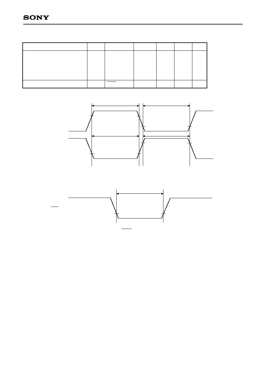
CXP836P60, CXP836P61
1
t
sys indicates the three values below according to the upper two bits (CPU clock selection) of the clock
control register (CLC: 00FEh).
t
sys [ns] = 2000/fc (upper two bits = "00"), 4000/fc (upper two bits = "01"), 16000/fc (upper two bits = "11").
EXTAL
t
XH
t
XL
t
CF
t
CR
0.4V
V
DD
≠ 0.4V
1/fc
Crystal oscillation
Ceramic oscillation
EXTAL
XTAL
External clock
EXTAL
XTAL
74HC04
C
1
C
2
TEX clock applied condition
Crystal oscillation
TEX
TX
C
1
C
2
TEX
EC
t
EH
t
EL
t
EF
t
ER
0.2V
DD
0.8V
DD
t
TH
t
TL
t
TF
t
TR
AC Characteristics
(1) Clock timing
System clock frequency
System clock input pulse
width
System clock input rise and
fall time
Event count input clock pulse
width
Event count input clock rise
and fall time
System clock frequency
Event count input clock input
pulse width
Event count input clock rise
and fall time
f
C
t
XL
,
t
XH
t
CR
,
t
CF
t
EH
,
t
EL
t
ER
,
t
EF
f
C
t
TL
,
t
TH
t
TR
,
t
TF
XTAL
EXTAL
EXTAL
EXTAL
EC
EC
TEX
TX
TEX
TEX
MHz
ns
ns
ns
ms
kHz
µs
ms
Item
Symbol
Pin
Conditions
Min.
Unit
Fig. 1, Fig. 2
Fig. 1, Fig. 2
external clock drive
Fig. 1, Fig. 2
external clock drive
Fig. 3
Fig. 3
V
DD
= 2.7 to 5.5V
Fig. 2 (32kHz clock
applied condition)
Fig. 3
Fig. 3
1
1
37.5
77.5
t
sys + 50
1
10
Typ.
32.768
Max.
10
5
200
20
20
(Ta = ≠20 to +75∞C, V
DD
= 2.7 to 5.5V, Vss = 0V)
Fig. 2. Clock applied conditions
Fig. 1. Clock timing
Fig. 3. Event count clock timing
V
DD
= 4.5 to 5.5V
V
DD
= 4.5 to 5.5V
≠ 20 ≠
CXP836P60, CXP836P61
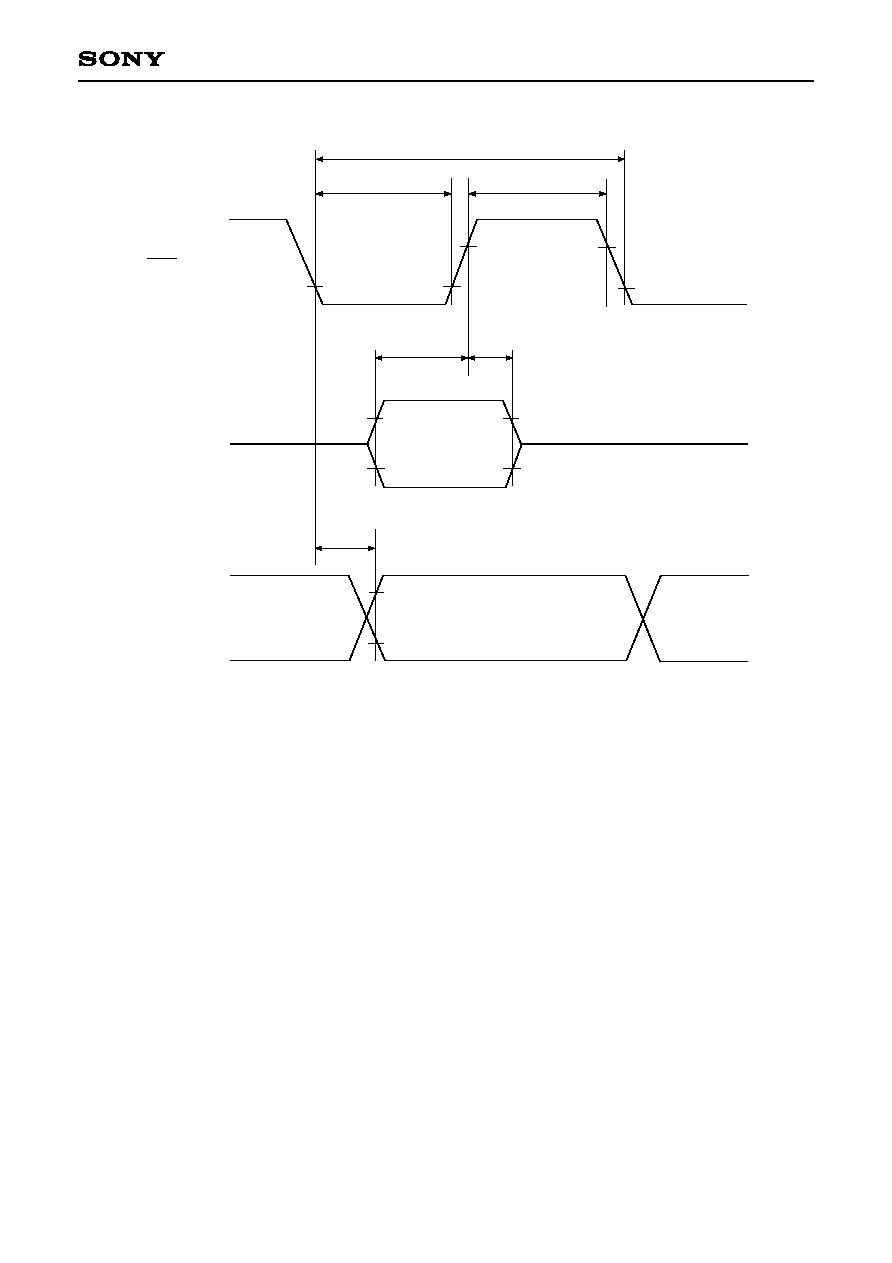
(2) Serial transfer (CH0)
(Ta = ≠20 to +75∞C, V
DD
= 4.5 to 5.5V, Vss = 0V)
CS
SCK
delay time
CS
SCK
float delay time
CS
SO
delay time
CS
SO
float delay time
CS high level width
t
sys + 200
2
t
sys + 200
16000/fc
t
sys + 100
8000/fc ≠ 100
≠
t
sys + 100
200
2
t
sys + 100
100
t
sys + 200
t
sys + 200
t
sys + 200
t
sys + 200
2
t
sys + 200
100
ns
ns
ns
ns
ns
ns
ns
ns
ns
ns
ns
ns
ns
ns
ns
Chip select transfer mode
(SCK = output mode)
Chip select transfer mode
(SCK = output mode)
Chip select transfer mode
Chip select transfer mode
Chip select transfer mode
Input mode
Output mode
Input mode
Output mode
SCK input mode
SCK output mode
SCK input mode
SCK output mode
SCK input mode
SCK output mode
SCK cycle time
SCK high and low
level widths
SI input setup time
(for SCK
)
SI input hold time
(for SCK
)
SCK
SO
delay time
t
DCSK
t
DCSKF
t
DCSO
t
DCSOF
t
WHCS
t
KCY
t
KH
t
KL
t
SIK
t
KSI
t
KSO
SCK0
SCK0
SO0
SO0
CS0
SCK0
SCK0
SI0
SI0
SO0
Note 1)
t
sys indicates the three values below according to the upper two bits (CPU clock selection) of the
clock control register (CLC: 00FEh).
t
sys [ns] = 2000/fc (upper two bits = "00"), 4000/fc (upper two bits = "01"), 16000/fc (upper two bits = "11")
Note 2) CS, SCK, SI and SO indicates CS0, SCK0, SI0 and SO0, respectively.
Note 3) The load condition for the SCK output mode, SO output delay time is 50pF + 1TTL.
Note 4) The value when Port B output buffer capability switching register (BUFB: 01F4h) selects buffer
capability to normal.
Item
Symbol
Pin
Min.
Max.
Unit
Conditions
≠ 21 ≠
CXP836P60, CXP836P61
Serial transfer (CH0)
(Ta = ≠20 to +75∞C, V
DD
= 2.7 to 3.3V, Vss = 0V)
CS
SCK
delay time
CS
SCK
float delay time
CS
SO
delay time
CS
SO
float delay time
CS high level width
t
sys + 200
2
t
sys + 200
16000/fc
t
sys + 100
8000/fc ≠ 150
≠
t
sys + 100
200
2
t
sys + 100
100
t
sys + 250
t
sys + 200
t
sys + 250
t
sys + 200
2
t
sys + 250
125
ns
ns
ns
ns
ns
ns
ns
ns
ns
ns
ns
ns
ns
ns
ns
Chip select transfer mode
(SCK = output mode)
Chip select transfer mode
(SCK = output mode)
Chip select transfer mode
Chip select transfer mode
Chip select transfer mode
Input mode
Output mode
Input mode
Output mode
SCK input mode
SCK output mode
SCK input mode
SCK output mode
SCK input mode
SCK output mode
SCK cycle time
SCK high and low
level widths
SI input setup time
(for SCK
)
SI input hold time
(for SCK
)
SCK
SO
delay time
t
DCSK
t
DCSKF
t
DCSO
t
DCSOF
t
WHCS
t
KCY
t
KH
t
KL
t
SIK
t
KSI
t
KSO
SCK0
SCK0
SO0
SO0
CS0
SCK0
SCK0
SI0
SI0
SO0
Item
Symbol
Pin
Min.
Max.
Unit
Conditions
Note 1)
t
sys indicates the three values below according to the upper two bits (CPU clock selection) of the
clock control register (CLC: 00FEh).
t
sys [ns] = 2000/fc (upper two bits = "00"), 4000/fc (upper two bits = "01"), 16000/fc (upper two bits = "11")
Note 2) CS, SCK, SI and SO indicates CS0, SCK0, SI0 and SO0, respectively.
Note 3) The load condition for the SCK output mode, SO output delay time is 50pF.
Note 4) The value when Port B output buffer capability switching register (BUFB: 01F4h) selects buffer
capability to high.
≠ 22 ≠
CXP836P60, CXP836P61
Fig. 4. Serial transfer CH0 timing
CS0
SCK0
0.2V
DD
0.8V
DD
t
WHCS
t
DCSK
t
DCSKF
0.8V
DD
0.2V
DD
0.8V
DD
t
KCY
t
KL
t
KH
0.8V
DD
0.2V
DD
SI0
t
SIK
t
KSI
Input data
t
DCSO
t
KSO
t
DCSOF
Output data
0.8V
DD
0.2V
DD
SO0
≠ 23 ≠
CXP836P60, CXP836P61
Serial Transfer (CH1)
(Ta = ≠20 to +75∞C, V
DD
= 4.5 to 5.5V, Vss = 0V)
1000
8000/fc
400
4000/fc ≠ 50
100
200
200
100
200
100
ns
ns
ns
ns
ns
ns
ns
ns
ns
ns
t
KCY
Input mode
Output mode
Input mode
Output mode
SCK input mode
SCK output mode
SCK input mode
SCK output mode
SCK input mode
SCK output mode
SCK1
t
KH
t
KL
SCK1
t
SIK
SI1
t
KSI
SI1
t
KSO
SO1
1000
8000/fc
400
4000/fc ≠ 100
100
200
200
100
250
125
ns
ns
ns
ns
ns
ns
ns
ns
ns
ns
t
KCY
Input mode
Output mode
Input mode
Output mode
SCK input mode
SCK output mode
SCK input mode
SCK output mode
SCK input mode
SCK output mode
t
KH
t
KL
t
SIK
t
KSI
t
KSO
SCK1
SCK1
SI1
SI1
SO1
Item
SCK cycle time
SCK high and low level
widths
SI input setup time
(for SCK
)
SI input hold time
(for SCK
)
SCK
SO delay time
Symbol
Pin
Conditions
Min.
Max.
Unit
Note 1)
t
sys indicates the three values below according to the upper two bits (CPU clock selection) of the
clock control register (CLC: 00FEh).
t
sys [ns] = 2000/fc (upper two bits = "00"), 4000/fc (upper two bits = "01"), 16000/fc (upper two bits = "11")
Note 2) SCK, SI and SO indicates SCK1, SI1 and SO1, respectively.
Note 3) The load condition for the SCK1 output mode, SO1 output delay time is 50pF + 1TTL.
Note 4) The value when Port B output buffer capability switching register (BUFB: 01F4h) selects buffer
capability to normal.
Serial Transfer (CH1)
(Ta = ≠20 to +75∞C, V
DD
= 2.7 to 3.3V, Vss = 0V)
Item
SCK cycle time
SCK high and low level
widths
SI input setup time
(for SCK
)
SI input hold time
(for SCK
)
SCK
SO delay time
Symbol
Pin
Conditions
Min.
Max.
Unit
Note 1)
t
sys indicates the three values below according to the upper two bits (CPU clock selection) of the
clock control register (CLC: 00FEh).
t
sys [ns] = 2000/fc (upper two bits = "00"), 4000/fc (upper two bits = "01"), 16000/fc (upper two bits = "11")
Note 2) SCK, SI and SO indicates SCK1, SI1 and SO1, respectively.
Note 3) The load condition for the SCK1 output mode, SO1 output delay time is 50pF.
Note 4) The value when Port B output buffer capability switching register (BUFB: 01F4h) selects buffer
capability to high.
≠ 24 ≠
CXP836P60, CXP836P61
t
KCY
t
KL
t
KH
0.2V
DD
0.8V
DD
t
SIK
t
KSI
t
KSO
Input data
Output data
0.2V
DD
0.8V
DD
0.2V
DD
0.8V
DD
SCK1
SI1
SO1
Fig. 5. Serial transfer CH1 timing
≠ 25 ≠
CXP836P60, CXP836P61
Conversion time
Sampling time
Analog input voltage
t
CONV
t
SAMP
V
IAN
V
ZT
1
V
FT
2
AN0 to AN7
Ta = 25∞C
V
DD
= 5.0V
V
SS
= 0V
Linearity error
Zero transition
voltage
Full-scale transition
voltage
Resolution
µs
µs
V
V
DD
31/f
ADC
3
10/f
ADC
3
0
Item
Symbol
Pin
Conditions
Min.
Typ.
Max.
Unit
Bits
(3) A/D converter characteristics
(Ta = ≠20 to +75∞C, V
DD
= 4.5 to 5.5V, Vss = 0V)
8
±3
LSB
70
mV
5030
10
4970
≠10
4910
mV
Conversion time
Sampling time
Analog input voltage
t
CONV
t
SAMP
V
IAN
V
ZT
1
V
FT
2
AN0 to AN7
Ta = 25∞C
V
DD
= 2.7V
V
SS
= 0V
Linearity error
Zero transition
voltage
Full-scale transition
voltage
Resolution
µs
µs
V
V
DD
31/f
ADC
3
10/f
ADC
3
0
Item
Symbol
Pin
Conditions
Min.
Typ.
Max.
Unit
Bits
(Ta = ≠20 to +75∞C, V
DD
= 2.7 to 3.3V, Vss = 0V)
8
±3
LSB
40
mV
2716
11
2688
≠10
2651
mV
Fig. 6. Definition of A/D converter terms
Analog input
Linearity error
V
FT
V
ZT
00h
01h
FEh
FFh
Digital conversion value
1
V
ZT
: Value at which the digital conversion value changes
from 00h to 01h and vice versa.
2
V
FT
: Value at which the digital conversion value changes
from FEh to FFh and vice versa.
3
f
ADC
= fc/4
≠ 26 ≠
CXP836P60, CXP836P61
External interruption
high and low level widths
Reset input low level width
INT0
INT1
INT2
INT3
INT4
RST
1
32/fc
µs
µs
t
IH
t
IL
t
RSL
(4) Interruption, reset input
(Ta = ≠20 to +75∞C, V
DD
= 2.7 to 5.5V, Vss = 0V)
0.2V
DD
0.8V
DD
t
IH
t
IL
t
IL
t
IH
INT0
INT1
INT2
INT3
INT4
Fig. 7. Interruption input timing
t
RSL
0.2V
DD
RST
Fig. 8. RST input timing
Item
Symbol
Pin
Conditions
Min.
Max.
Unit
≠ 27 ≠
CXP836P60, CXP836P61
Appendix
C
1
EXTAL
XTAL
C
2
Rd
EXTAL
XTAL
(i) Main clock
EXTAL
XTAL
C
1
C
2
Rd
XTAL
(ii) Main clock
EXTAL
XTAL
C
1
C
2
Rd
TEX
TX
(iii) Sub clock
Fig. 9. SPC700 series recommended oscillation circuit
1
Those marked with an
1
signify types with
built-in ground capacitance (C
1
, C
2
).
Manufacturer
MURATA MFG
CO., LTD.
RIVER
ELETEC
CO., LTD.
KINSEKI LTD.
Model
CSA4.19MG
CSA8.00MG
CST4.19MGW
1
CST8.00MTW
1
HC-49/U03
CX-5F
FCR4.19MC5
1
FCR8.0MC5
1
FCR10.0MC5
1
CCR4.19MC3
1
CCR8.0MC5
1
CCR10.0MC5
1
TDK
Corporation
Seiko
Instruments Inc.
VTC-200
SP-T
fc (MHz)
4.19
8.00
10.00
4.19
8.00
10.00
4.19
8.00
10.00
4.19
8.00
10.00
4.19
8.00
10.00
4.19
8.00
10.00
32.768
75.00
C
1
(pF)
C
2
(pF)
Rd (
)
100
30
30
100
30
30
22
15
10
33
18
15
30 ( ± 20%)
20 ( ± 20%)
20 ( ± 20%)
36 ( ± 20%)
20 ( ± 20%)
20 ( ± 20%)
18
4
100
30
30
100
30
30
22
15
10
33
18
15
30 ( ± 20%)
20 ( ± 20%)
20 ( ± 20%)
36 ( ± 20%)
20 ( ± 20%)
20 ( ± 20%)
18
4
0
0
0
0
0
0
1.0k
100
100
2.2k
0
0
0
330k
100k
Circuit
example
(i)
CSA10.0MT
(ii)
CST10.00MTW
1
(i)
(ii)
(iii)
Remarks
CL = 12.5pF
CL = 6.0pF
FCR
: Lead-type ceramic oscillator
CCR
: Surface mounted-type ceramic oscillator
CL
: Load Capacitor
Product List
Item
Package
ROM
capacity
RST pin pull-up
resistor
Products
Mask
PROM
CXP
83508
CXP
83512
CXP
83516
CXP
83620
CXP
83624
CXP
83509
CXP
83513
CXP
83517
CXP
83621
CXP
83625
CXP836P60Q
-1-
CXP836P60R
-1-
CXP836P61Q
-1-
80-pin plastic
QFP/LQFP
0.65mm pitch
80-pin plastic QFP
80-pin plastic
QFP
80-pin plastic
LQFP
80-pin plastic
QFP (0.65mm pitch)
PROM 60K
bytes
Existent
8K
bytes
12K
bytes
16K
bytes
20K
bytes
24K
bytes
8K
bytes
12K
bytes
16K
bytes
20K
bytes
24K
bytes
Existent/Non-existent
CL = 12.0pF
CL = 12.0pF
CL = 12.0pF
≠ 28 ≠
CXP836P60, CXP836P61
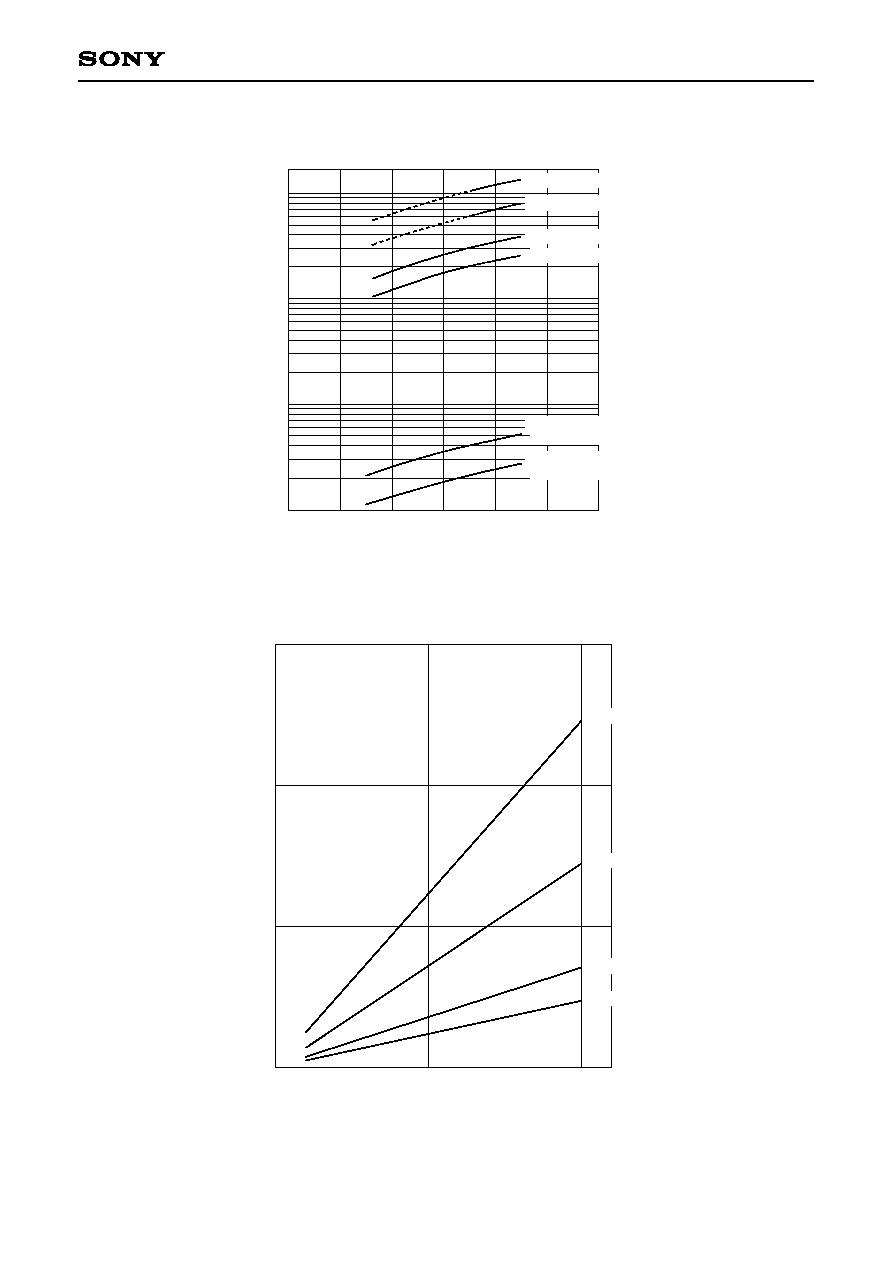
10.0
1.0
0.1
(100µA)
0.01
(10µA) 1
2
3
4
5
6
7
I
DD
vs. V
DD
(fc = 10MHz, Ta = 25∞C, typical)
V
DD
≠ Supply voltage [V]
I
DD
≠
Supply current [mA]
5.0
0.5
0.05
(50µA)
1/2 frequency dividing mode
32kHz mode
(instruction)
32kHz
Sleep mode
1/4 frequency dividing mode
Sleep mode
1/16 frequency dividing mode
0
5
10
0
5
10
15
1/2 frequency dividing mode
1/4 frequency dividing mode
1/16 frequency dividing mode
Sleep mode
I
DD
vs. fc
(V
DD
= 5V, Ta = 25∞C, typical)
fc ≠ System clock [MHz]
I
DD
≠
Supply current [mA]
Characteristics Curve
≠ 29 ≠
CXP836P60, CXP836P61
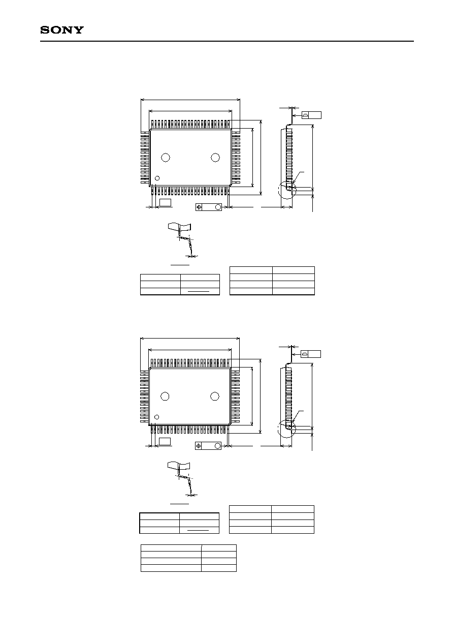
PACKAGE STRUCTURE
SONY CODE
EIAJ CODE
JEDEC CODE
QFP-80P-L01
QFP080-P-1420
PACKAGE MATERIAL
LEAD TREATMENT
LEAD MATERIAL
PACKAGE MASS
EPOXY RESIN
SOLDER PLATING
42/COPPER ALLOY
1.6g
23.9
±
0.4
20.0 ≠ 0.1
+ 0.4
1
80
65
64
41
40
25
24
0.8
0.35 ≠ 0.1
+ 0.15
14.0 ≠ 0.1
+ 0.4
17.9
±
0.4
16.3
0.1 ≠ 0.05
+ 0.2
2.75 ≠ 0.15
+ 0.35
0.8
±
0.2
0.15 ≠ 0.05
+ 0.1
80PIN QFP (PLASTIC)
M
0.2
0.15
0∞ to 10∞
DETAIL A
A
Package Outline
Unit: mm
CXP836P60
PACKAGE STRUCTURE
SONY CODE
EIAJ CODE
JEDEC CODE
QFP-80P-L01
QFP080-P-1420
PACKAGE MATERIAL
LEAD TREATMENT
LEAD MATERIAL
PACKAGE MASS
EPOXY RESIN
SOLDER PLATING
42/COPPER ALLOY
1.6g
23.9
±
0.4
20.0 ≠ 0.1
+ 0.4
1
80
65
64
41
40
25
24
0.8
0.35 ≠ 0.1
+ 0.15
14.0
≠
0.1
+ 0.4
17.9
±
0.4
16.3
0.1 ≠ 0.05
+ 0.2
2.75 ≠ 0.15
+ 0.35
0.8
±
0.2
0.15 ≠ 0.05
+ 0.1
80PIN QFP (PLASTIC)
M
0.2
0.15
0∞ to 10∞
DETAIL A
A
CXP836P60
LEAD PLATING SPECIFICATIONS
ITEM
LEAD MATERIAL
42 ALLOY
SOLDER COMPOSITION
Sn-Bi Bi:1-4wt%
PLATING THICKNESS
5-18
µ
m
SPEC.
≠ 30 ≠
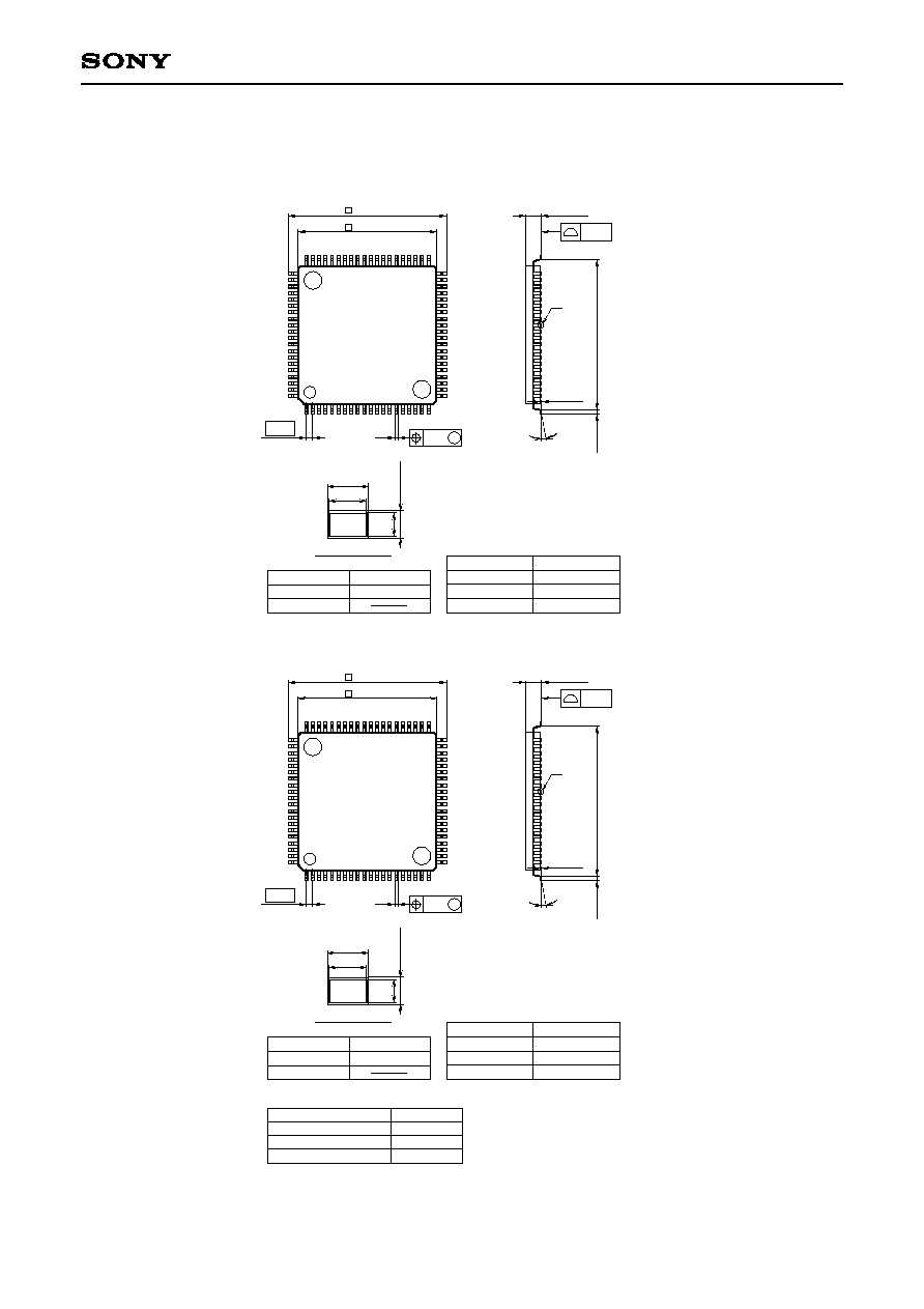
CXP836P60, CXP836P61
SONY CODE
EIAJ CODE
JEDEC CODE
PACKAGE STRUCTURE
PACKAGE MATERIAL
LEAD TREATMENT
LEAD MATERIAL
PACKAGE MASS
EPOXY RESIN
42 / COPPER ALLOY
QFP-80P-L03
P-QFP80-14x14-0.65
0.6g
80PIN QFP (PLASTIC)
16.0
±
0.4
14.0 ≠ 0.1
+ 0.4
b
0∞ to 10∞
0.5
±
0.2
0.1 ≠ 0.1
+ 0.15
(15.0)
1.5 ≠ 0.15
+ 0.35
40
21
20
1
41
60
61
80
M
0.24
0.1
0.65
b = 0.3 ≠ 0.1
( 0.3 )
(0.127)
+ 0.15
0.127
≠
0.05
+ 0.1
DETAIL A : SOLDER
A
SOLDER PLATING
Package Outline
Unit: mm
CXP836P61
SONY CODE
EIAJ CODE
JEDEC CODE
PACKAGE STRUCTURE
PACKAGE MATERIAL
LEAD TREATMENT
LEAD MATERIAL
PACKAGE MASS
EPOXY RESIN
42 / COPPER ALLOY
QFP-80P-L03
P-QFP80-14x14-0.65
0.6g
80PIN QFP (PLASTIC)
16.0
±
0.4
14.0 ≠ 0.1
+ 0.4
b
0∞ to 10∞
0.5
±
0.2
0.1 ≠ 0.1
+ 0.15
(15.0)
1.5 ≠ 0.15
+ 0.35
40
21
20
1
41
60
61
80
M
0.24
0.1
0.65
b = 0.3 ≠ 0.1
( 0.3 )
(0.127)
+ 0.15
0.127
≠
0.05
+ 0.1
DETAIL A : SOLDER
A
SOLDER PLATING
LEAD PLATING SPECIFICATIONS
ITEM
LEAD MATERIAL
42 ALLOY
SOLDER COMPOSITION
Sn-Bi Bi:1-4wt%
PLATING THICKNESS
5-18
µ
m
SPEC.
CXP836P61
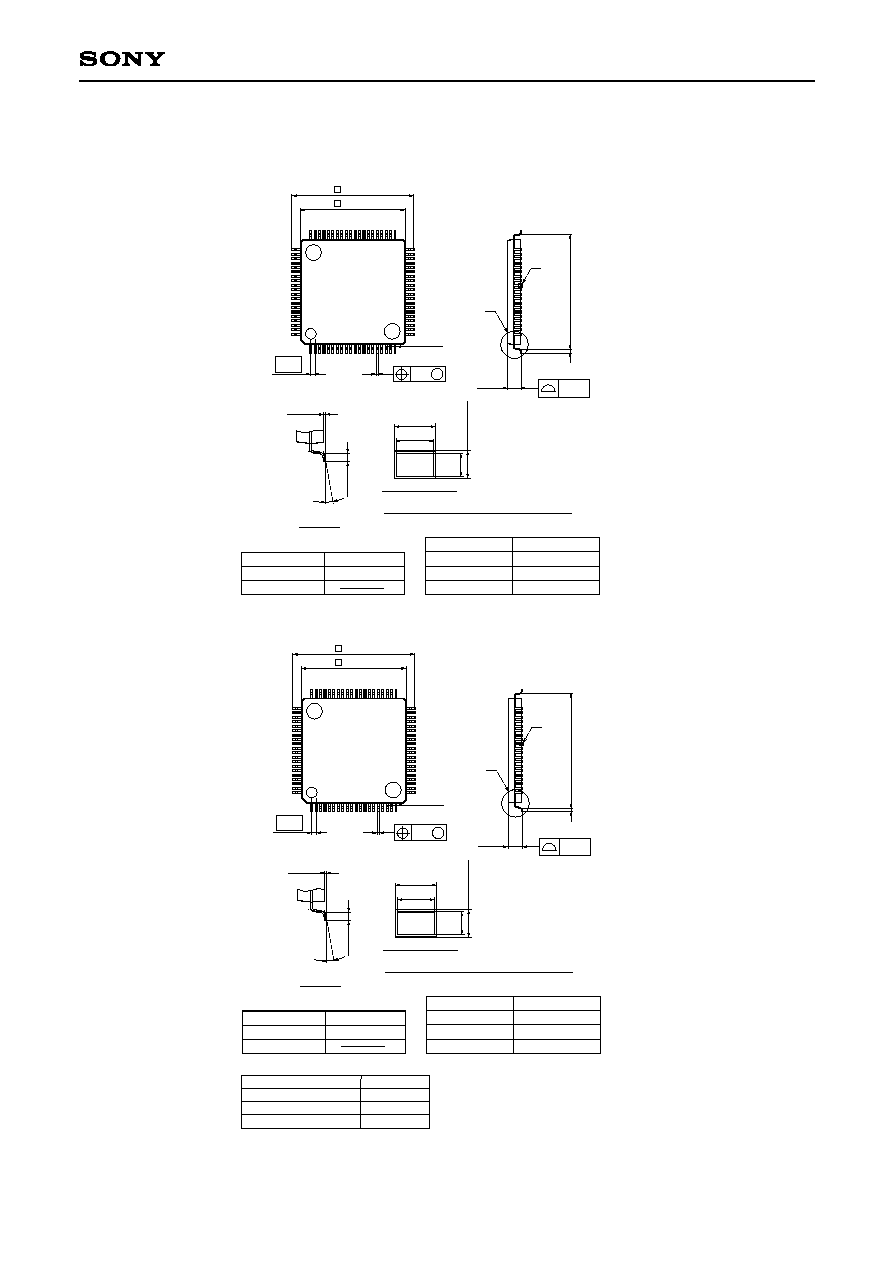
≠ 31 ≠
CXP836P60, CXP836P61
20
21
40
41
60
61
80
1
SONY CODE
EIAJ CODE
JEDEC CODE
PACKAGE MATERIAL
LEAD TREATMENT
LEAD MATERIAL
PACKAGE MASS
EPOXY RESIN
SOLDER PLATING
42 / COPPER ALLOY
PACKAGE STRUCTURE
14.0
±
0.2
12.0
±
0.1
(0.22)
b
A
1.5 ≠ 0.1
+ 0.2
0.5
±
0.2
(13.0)
80PIN LQFP (PLASTIC)
0.5g
LQFP-80P-L01
P-LQFP80-12x12-0.5
0.1
NOTE: Dimension "
" does not include mold protrusion.
0.13 M
0.5
b = 0.18 ≠ 0.03
( 0.18 )
(0.127)
+ 0.08
0.127
≠
0.02
+ 0.05
DETAIL B : SOLDER
DETAIL A
0∞ to 10∞
0.1
±
0.1
0.5
±
0.2
B
Package Outline
Unit: mm
CXP836P60
20
21
40
41
60
61
80
1
SONY CODE
EIAJ CODE
JEDEC CODE
PACKAGE MATERIAL
LEAD TREATMENT
LEAD MATERIAL
PACKAGE MASS
EPOXY RESIN
SOLDER PLATING
42 / COPPER ALLOY
PACKAGE STRUCTURE
14.0
±
0.2
12.0
±
0.1
(0.22)
b
A
1.5 ≠ 0.1
+ 0.2
0.5
±
0.2
(13.0)
80PIN LQFP (PLASTIC)
0.5g
LQFP-80P-L01
P-LQFP80-12x12-0.5
0.1
NOTE: Dimension "
" does not include mold protrusion.
0.13 M
0.5
b = 0.18 ≠ 0.03
( 0.18 )
(0.127)
+ 0.08
0.127
≠
0.02
+ 0.05
DETAIL B : SOLDER
DETAIL A
0∞ to 10∞
0.1
±
0.1
0.5
±
0.2
B
LEAD PLATING SPECIFICATIONS
ITEM
LEAD MATERIAL
42 ALLOY
SOLDER COMPOSITION
Sn-Bi Bi:1-4wt%
PLATING THICKNESS
5-18
µ
m
SPEC.
CXP836P60
Sony Corporation