CMOS 8-bit Single-chip Microcomputer
Description
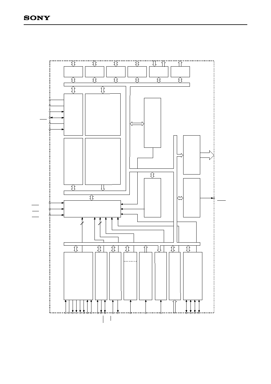
The CXP85112B/85116B, CXP85220A/85224A/
85228A/85232A is a CMOS 8-bit single chip
microcomputer integrating on a single chip an A/D
converter, serial interface, timer/counter, time base
timer, vector interruption, on-screen display function,
I
2
C bus interface, PWM generator, remote control
reception circuit, HSYNC counter, power source
frequency counter and watch dog timer besides the
basic configurations of 8-bit CPU, ROM, RAM, and
l/O port.
The CXP85112B/85116B, CXP85220A/85224A/
85228A/85232A also provides a power-on reset
function and a sleep function that enables lower
power consumption.
Features
∑ Wide-range instruction system (213 instructions) to cover various types of data
-- 16-bit arithmetic/multiplication and division/boolean bit operation instructions
∑ Minimum instruction cycle
1µs at 4MHz operation
∑ Incorporated ROM capacity
12K bytes (CXP85112B)
16K bytes (CXP85116B)
20K bytes (CXP85220A)
24K bytes (CXP85224A)
28K bytes (CXP85228A)
32K bytes (CXP85232A)
∑ Incorporated RAM capacity
352 bytes (CXP85112B/85116B)
448 bytes (CXP85220A/85224A/85228A/85232A)
∑ Peripheral functions
-- On-screen display function
12
◊
16 dots, 128 types
21 words
◊
4 Iines (more than 4 Iines possible)
Double scan mode compatible, jitter elimination circuit
-- I
2
C bus interface
-- PWM output
14 bits, 1 channel
6 bits, 8 channels
-- Remote control reception circuit
8-bit pulse measurement counter with on-chip 6-stage FIFO
-- A/D converter
4 bits, 4channels, successive approximation method
(Conversion time of 40µs/4MHz)
-- HSYNC counter
-- Power supply frequency counter
-- Watch dog timer
-- Serial I/O
8-bit clock synchronization
-- Timer
8-bit timer, 8-bit timer/counter, 19-bit time base timer
∑ Interruption
14 factors, 14 vectors, multi-interruption possible
∑ Standby mode
Sleep
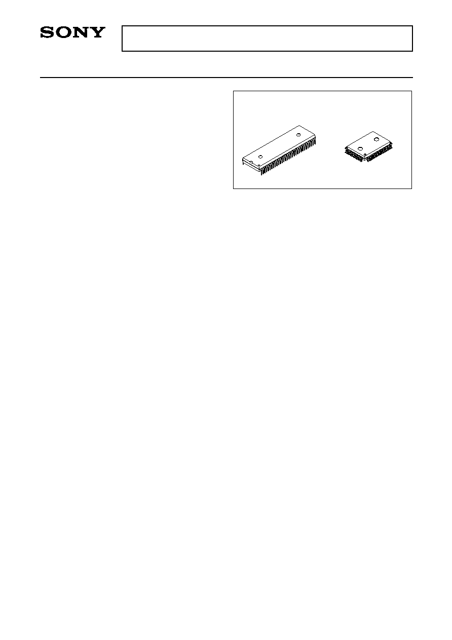
∑ Package
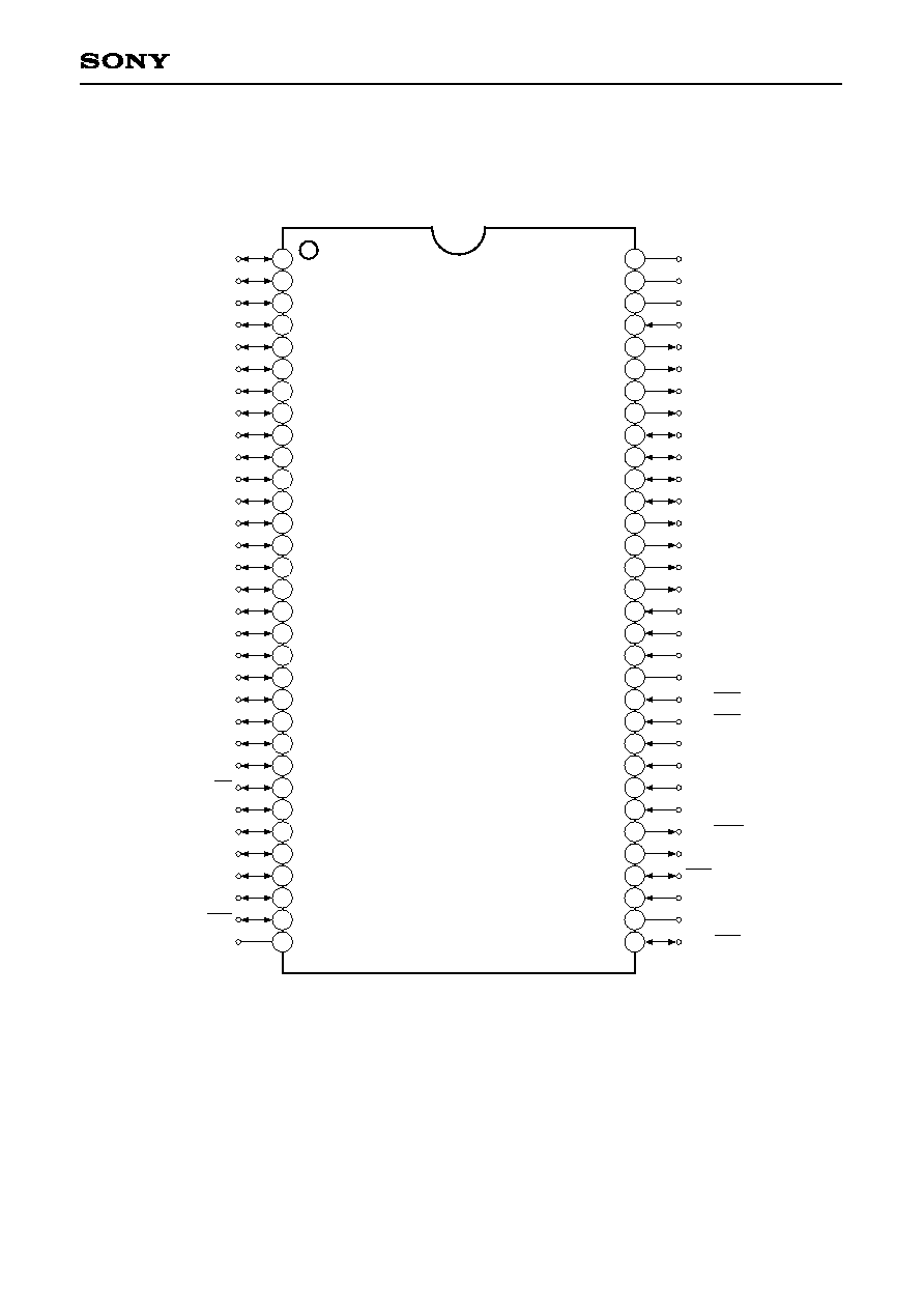
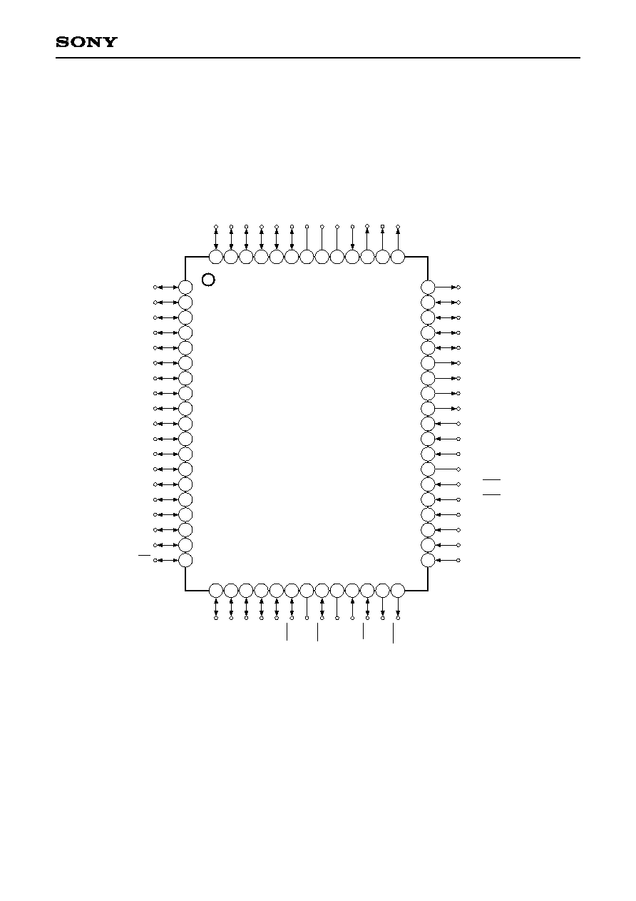
64-pin plastic SDIP/QFP
∑ Piggyback/evaluation chip
CXP85100A, CXP85190 (Custom font compatible)
CXP85200A, CXP85290 (Custom font compatible)
≠ 1 ≠
E93Z17B86
Sony reserves the right to change products and specifications without prior notice. This information does not convey any license by
any implication or otherwise under any patents or other right. Application circuits shown, if any, are typical examples illustrating the
operation of the devices. Sony cannot assume responsibility for any problems arising out of the use of these circuits.
CXP85112B/85116B
CXP85220A/85224A/85228A/85232A
64 pin SDIP (Plastic)
64 pin QFP (Plastic)
Structure
Silicon gate CMOS IC
Purchase of Sony's I
2
C components conveys a license under the Philips I
2
C Patent Rights to use these components
in an I
2
C system, provided that the system conforms to the I
2
C Standard Specifications as defined by Philips.
≠ 5 ≠
CXP85112B/85116B, CXP85220A/85224A/85228A/85232A
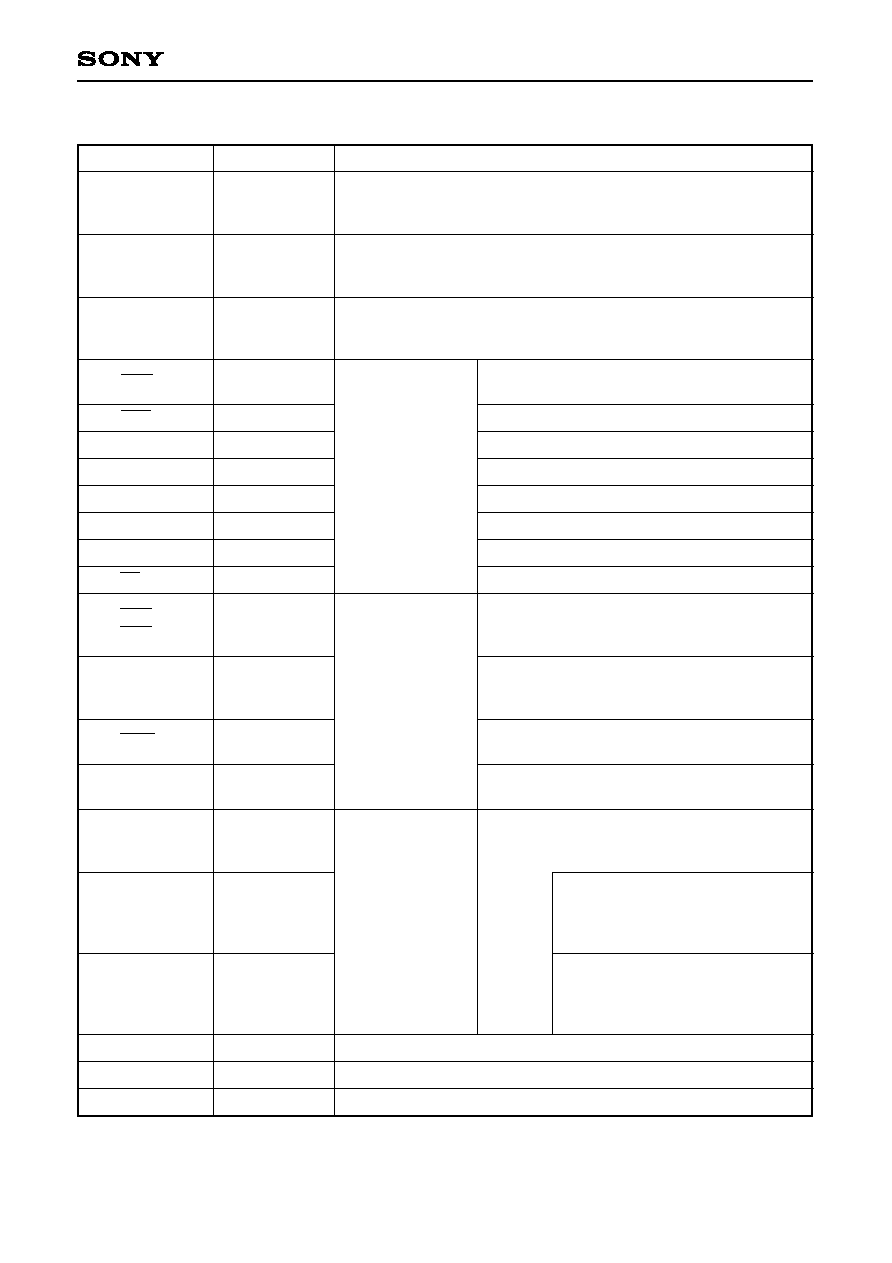
(Port A)
8-bit I/O port. I/O can be set in a unit of single bits.
(8 pins)
(Port B)
8-bit I/O port. I/O can be set in a unit of single bits.
(8 pins)
(Port C)
8-bit I/O port. I/O can be set in a unit of single bits.
(8 pins)
(Port D)
8-bit I/O port.
I/O can be set ina a
unit of single bits.
Capable of driving
12mA sink current.
(8 pins)
(Port E)
8-bit port. Lower
6 bits are for inputs;
upper 2 bits are for
outputs.
(Port F)
8-bit output port,
operating as N-ch
open drain output
for high current
(12mA).
Lower 4 bits are
medium voltage
drive outputs (12V),
upper 4bits are 5V
drive outputs.
(8 pins)
4-bit outputs for CRT display.
Horizontal synchronizing signal input for CRT display.
Vertical synchronizing signal input for CRT display.
Pin Description
Symbol
PA0 to PA7
PB0 to PB7
PC0 to PC7
PD0/INT2
PD1/SCK
PD2/SO
PD3/SI
PD4/HSI
PD5/ACI
PD6/RMC
PD7/EC
PE0/INT0
PE1/INT1
PE2/AN0
to
PE5/AN3
PE6/PWM
PE7/TO
PF0/PWM0
to
PF3/PWM3
PF4/PWM4/
SCL0
PF5/PWM5/
SCL1
PF6/PWM6/
SDA0
PF7/PWM7/
SDA1
R, G, B, BLK
HSYNC
VSYNC
I/O
I/O
I/O
I/O/Input
I/O/I/O
I/O/Output
I/O/Input
I/O/Input
I/O/Input
I/O/Input
I/O/Input
Input/Input
Input/Input
Output/Output
Output/Output
Output/Output
Output/Output/
I/O
Output/Output/
I/O
Output
Input
Input
I/O
Description
External interruption request input.
Active at falling edge.
Serial clock I/O.
Serial data output.
Serial data input.
HSYNC counter input.
Input for power supply frequency counter.
Input for remote control reception circuit.
External event input for timer/counter.
External interruption request inputs.
Active at falling edge.
(2 pins)
Analog inputs for A/D converter.
(4 pins)
14-bit PWM output.
(CMOS output)
Rectangular waveform output for Timer 1.
(Duty output 50%)
6-bit PWM outputs.
(8 pins)
Transfer clock I/Os for I
2
C bus
interface.
Transfer data I/Os for I
2
C data bus.