 | –≠–ª–µ–∫—Ç—Ä–æ–Ω–Ω—ã–π –∫–æ–º–ø–æ–Ω–µ–Ω—Ç: CXP88452 | –°–∫–∞—á–∞—Ç—å:  PDF PDF  ZIP ZIP |
CXP88452/88460
CMOS 8-bit Single Chip Microcomputer
Description
The CXP88452/88460 is a CMOS 8-bit microcomputer
which consists of A/D converter, serial interface,
timer/counter, time-base timer, high precision timing
pattern generation circuit, PWM output, VISS/VASS
circuit, 32kHz timer/counter, remote control receiving
circuit, VSYNC separator and the measurement circuit
which measure signals of capstan FG and drum
FG/PG and other servo systems, as well as basic
configurations like 8-bit CPU, ROM, RAM and I/O
port. They are integrated into a single chip.
Also, the CXP88452/88460 provides sleep/stop
functions which enable to lower power consumption.
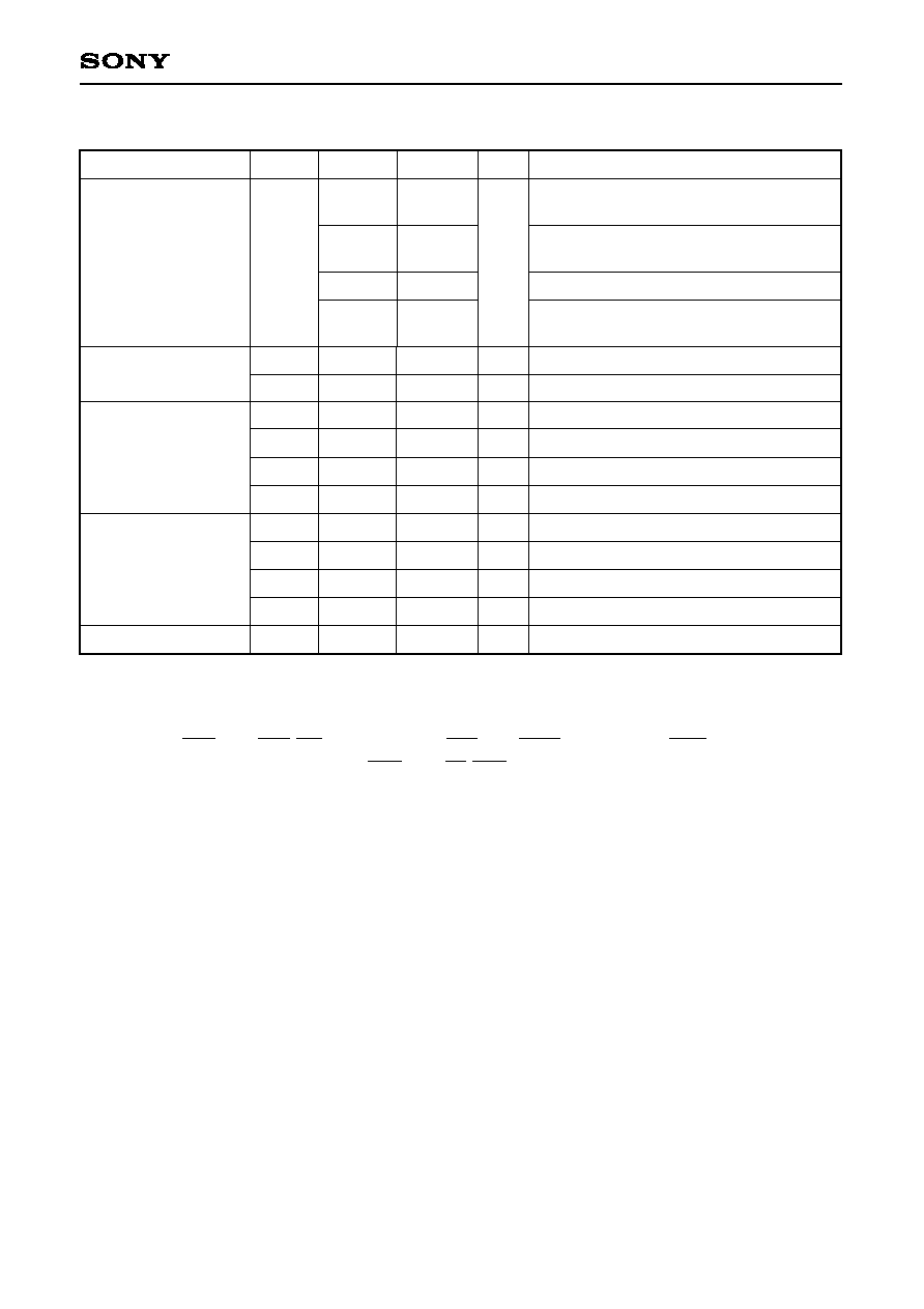
Features
∑ A wide instruction set (213 instructions) which covers various types of data
-- 16-bit arithmetic/multiplication and division/boolean bit operation instructions
∑ Minimum instruction cycle
250ns at 16MHz operation
122µs at 32kHz operation
∑ Incorporated ROM capacity
52K bytes (CXP88452)
60K bytes (CXP88460)
∑ Incorporated RAM capacity
2048 bytes
∑ Peripheral functions
-- A/D converter
8 bits, 12 channels, successive approximation system
(Conversion time of 20µs/16MHz)
-- Serial interface
Incorporated 8-bit, 8-stage FIFO
(Auto transfer for 1 to 8 bytes), 1 channel
Incorporated buffer RAM (Auto transfer for 1 to 32 bytes), 1 channnel
Incorporated two-wire 8-bit and 8-stage FIFO (Auto transfer for
1 to 8 bytes), 1 channel
-- Timer
8-bit timer/counter, 2 channels
19-bit time-base timer
32kHz timer/counter
-- High precision timing pattern generation
PPG: Maximum of 19 pins 32 stages programmable
circuit
RTG: 5 pins, 1 channel
7-bit, 10-satge FIFO (RECCTL control/ATC control),
1channel
-- PWM/DA gate output
PWM: 12 bits, 2 channels (Repetitive frequency 62.5kHz at 16MHz)
DA gate pulse output: 13 bits, 2 channels
-- Analog signal input circuit
PBCTL amplifier circuit
Reel FG comparator
-- CTL write/rewrite circuit
Recording current control circuit
-- Servo input control
Capstan FG, Drum FG/PG, CTL, Reel FG input
-- VSYNC separator
-- FRC capture unit
Incorporated 26-bit and 8-stage FIFO
-- PWM output
14 bits, 1 channel
-- VISS/VASS circuit
Pulse duty auto detection circuit
-- Remote control receiving circuit
8-bit pulse measurement counter, 6-stage FIFO
-- Tri-state output
PPG output 2 pins
-- High speed head switching circuit
∑ Interruption
22 factors, 15 vectors, multi-interruption possible
∑ Standby mode
Sleep/stop
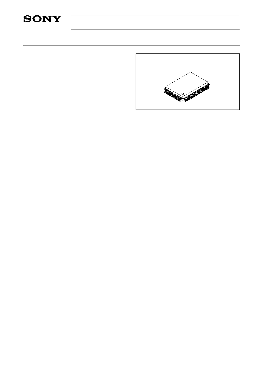
∑ Package
100-pin plastic QFP
∑ Piggy/evaluation chip
CXP88400 100-pin ceramic PQFP
≠ 1 ≠
E98772-PS
Sony reserves the right to change products and specifications without prior notice. This information does not convey any license by
any implication or otherwise under any patents or other right. Application circuits shown, if any, are typical examples illustrating the
operation of the devices. Sony cannot assume responsibility for any problems arising out of the use of these circuits.
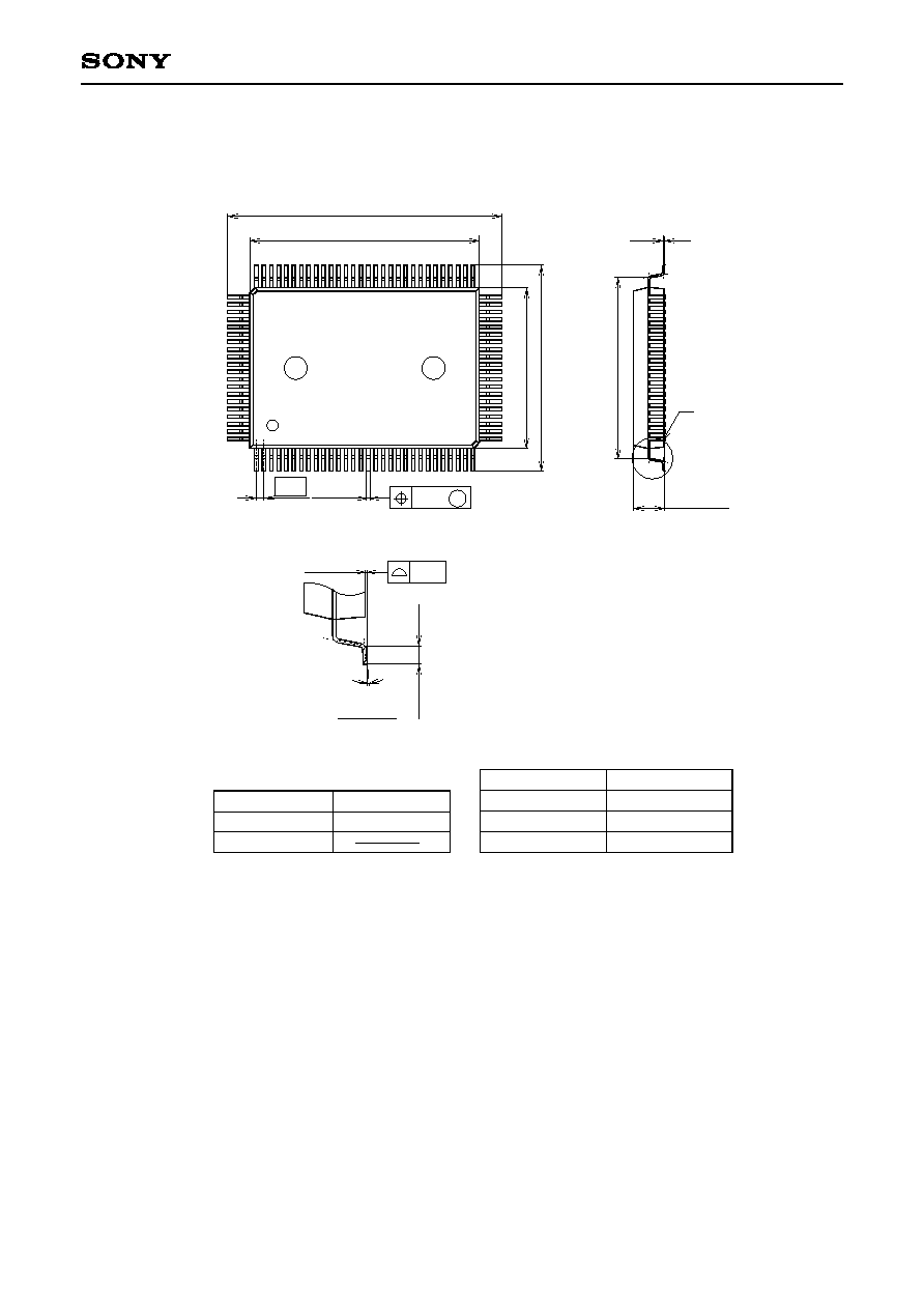
100 pin QFP (Plastic)
Structure
Silicon gate CMOS IC
≠ 2 ≠
CXP88452/88460
P
A
0
t
o
P
A
7
P
B
0
t
o
P
B
7
P
C
0
t
o
P
C
7
P
D
0
t
o
P
D
7
P
E
0
,
1
,
6
,
7
P
E
2
t
o
P
E
5
P
F
0
t
o
P
F
3
P
F
4
t
o
P
F
7
P
G
0
t
o
P
G
3
P
I
0
t
o
P
I
7
RS
T
EX
TA
L
C
L
O
C
K
G
E
N
E
R
A
T
O
R
/
S
Y
S
T
E
M
C
O
N
T
R
O
L
R
A
M
2
0
4
8
B
Y
T
E
S
S
P
C
7
0
0
C
P
U
C
O
R
E
R
O
M
5
2
K
/
6
0
K
B
Y
T
E
S
IN
TE
RR
UP
T C
ON
TR
OL
LE
R
2
F
I
F
O
F
R
C
C
A
P
T
U
R
E
U
N
I
T
AV
ss
AV
RE
F
AV
DD
A
/
D
C
O
N
V
E
R
T
E
R
S
E
R
I
A
L
I
N
T
E
R
F
A
C
E
U
N
I
T
(
C
H
2
)
F
I
F
O
S
C
L
0
A
N
0
t
o
A
N
1
1
IN
T2
IN
T0
1
2
8
PO
RT
A
8
PO
RT
B
8
PO
RT
C
PO
RT
D
6
2
PO
RT
E
4
4
PO
RT
F
4
PO
RT
G
4
PO
RT
H
8
PO
RT
I
P
H
4
t
o
P
H
7
Vs
s
V
DD
MP
XT
AL
TX
TE
X
IN
T1
/N
MI
P
R
E
S
C
A
L
E
R
/
T
I
M
E
-
B
A
S
E
T
I
M
E
R
3
2
k
H
z
T
I
M
E
R
/
C
O
U
N
T
E
R
8
8
-
B
I
T
T
I
M
E
R
/
C
O
U
N
T
E
R
0
V
S
Y
N
C
S
E
P
A
R
A
T
O
R
8
-
B
I
T
T
I
M
E
R
1
S
O
1
R
M
C
C
T
L
F
A
M
P
I
S
Y
N
C
E
C
S
C
K
1
S
I
1
T
O
/
D
D
O
N
M
I
2
2
2
5
2
5
S
E
R
I
A
L
I
N
T
E
R
F
A
C
E
U
N
I
T
(
C
H
0
)
R
A
M
S
E
R
I
A
L
I
N
T
E
R
F
A
C
E
U
N
I
T
(
C
H
1
)
F
I
F
O
D
A
A
1
D
A
A
0
1
4
-
B
I
T
P
W
M
G
E
N
E
R
A
T
O
R
1
2
-
B
I
T
P
W
M
G
E
N
E
R
A
T
O
R
C
H
0
S
E
R
V
O
I
N
P
U
T
C
O
N
T
R
O
L
1
2
-
B
I
T
P
W
M
G
E
N
E
R
A
T
O
R
C
H
1
V
I
S
S
/
V
A
S
S
R
E
M
O
C
O
N
I
N
P
U
T
F
I
F
O
C
T
L
R
/
W
C
O
N
T
R
O
L
P
W
M
1
P
W
M
0
P
W
M
D
P
G
D
F
G
C
F
G
E
X
I
1
E
X
I
0
H
E
A
D
L
C
T
L
H
E
A
D
A
D
J
C
A
P
S
T
A
I
N
D
R
U
M
P
B
C
T
L
A
M
P
R
E
E
L
C
O
M
P
A
R
A
T
O
R
S
C
L
1
S
D
A
0
S
D
A
1
C
S
0
S
I
0
S
O
0
S
C
K
0
R
F
G
0
R
F
G
1
4
2
1
9
5
P
R
O
G
R
A
M
A
B
L
E
P
A
T
T
E
R
N
G
E
N
E
R
A
T
O
R
R
A
M
R
E
A
L
T
I
M
E
P
U
L
S
E
G
E
N
E
R
A
T
O
R
C
H
0
C
H
1
F
I
F
O
P
H
0
t
o
P
H
3
PP
O0
to
PP
O1
8
RT
O3
to
RT
O7
4
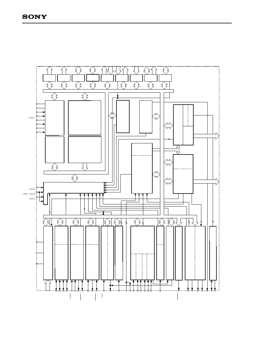
Block Diagram
≠ 3 ≠
CXP88452/88460
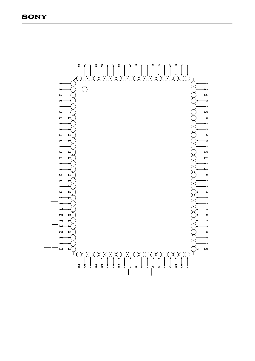
Pin Assignment (Top View)
PE5/EXI1
P
H
7
40
39
38
37
36
35
34
31 32 33
41 42 43 44 45 46 47 48 49 50
51
52
53
54
55
56
57
58
59
60
70
69
68
67
63
64
65
66
61
62
71
72
73
74
75
76
77
78
79
80
2
3
4
5
6
7
8
9
10
11
12
13
14
15
16
17
18
19
20
21
22
23
24
25
26
27
28
29
30
1
81
82
83
84
88 87 86 85
89
90
100 99 98 97 96 95 94
91
92
93
PE6/PWM0/DAA0
PE7/PWM1/DAA1
RFG0
RFG1
ANOUT
AMPV
DD
CTLFAMPO
CTLSAMPI
CTLAGND
CTLFAMPI (≠)
CTLFAMPI (+)
HEADL (≠)
HEADL (+)
CTLHEAD (+)
CTLHEAD (≠)
AMPV
SS
V
DD
AN0
AN1
AN2
AN3
PF0/AN4
PF1/AN5
PF2/AN6
PF3/AN7
AV
DD
AV
REF
AV
SS
PF4/AN8
P
H
6
P
H
5
P
H
4
P
H
3
/
S
D
A
1
P
H
2
/
S
D
A
0
P
H
1
/
S
C
L
1
P
H
0
/
S
C
L
0
M
P
R
S
T
V
S
S
X
T
A
L
E
X
T
A
L
P
G
3
/
E
C
/
I
N
T
2
P
G
2
/
D
P
G
P
G
1
/
D
F
G
P
G
0
/
C
F
G
P
F
7
/
A
N
1
1
P
F
6
/
A
N
1
0
P
F
5
/
A
N
9
PB5/PPO13
PB4/PPO12
PB3/PPO11
PB2/PPO10
PB1/PPO9
PB0/PPO8
PC7/RTO7
PC6/RTO6
PC5/RTO5
PC4/RTO4
PC3/RTO3
PC2/PPO18
PC1/PPO17
PC0/PPO16
PI7
PI6
PI5
PI4
PI3
PI2
PI1
PI0/INT0
PD7/SI0
PD6/SO0
PD5/SCK0
PD4/CS0
PD3/SRVO/TO/DDO/ADJ
PD2/PWM
PD1/RMC
PD0/INT1/NMI
P
B
6
/
P
P
O
1
4
P
B
7
/
P
P
O
1
5
P
A
0
/
P
P
O
0
P
A
1
/
P
P
O
1
P
A
2
/
P
P
O
2
P
A
3
/
P
P
O
3
P
A
4
/
P
P
O
4
P
A
5
/
P
P
O
5
P
A
6
/
P
P
O
6
P
A
7
/
P
P
O
7
N
C
V
D
D
V
S
S
T
X
T
E
X
P
E
0
/
S
C
K
1
P
E
1
/
S
O
1
P
E
2
/
S
I
1
P
E
3
/
S
Y
N
C
P
E
4
/
E
X
I
0
Note) 1. NC (Pin 90) is always connected to V
DD
.
2. V
DD
(Pins 63 and 89) are both connected to V
DD
3. Vss (Pins 41 and 88) are both connected to GND.
4. MP (Pin 39) is always connected to GND.
≠ 4 ≠
CXP88452/88460
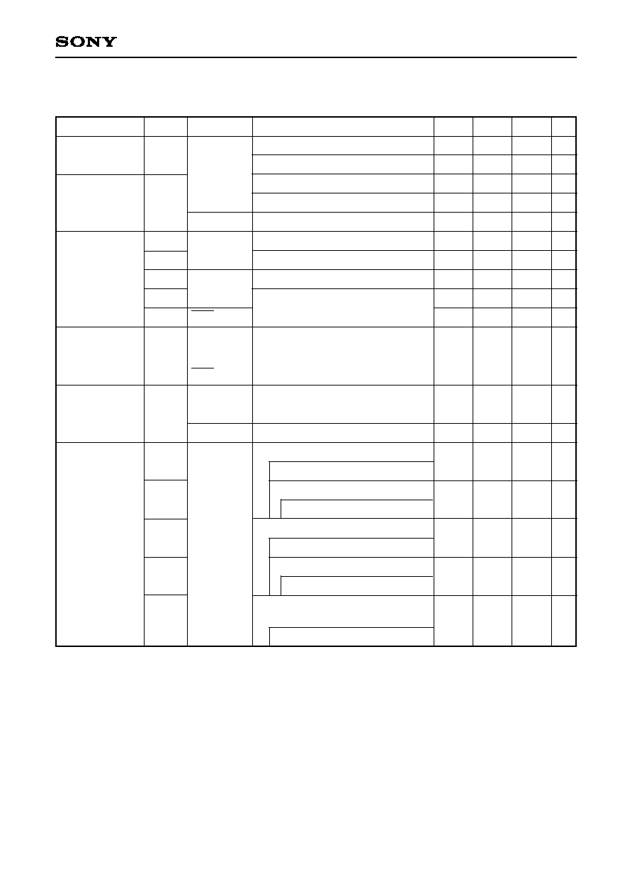
Pin Description
(Port A)
8-bit output port. Data is
gated with PPO contents
by OR-gate and they are
output.
(8 pins)
(Port B)
8-bit output port. Data is
gated with PPO contents
by OR-gate and they are
output.
(8 pins)
(Port C)
8-bit I/O port. I/O can be
set in a unit of single bits.
Data is gated with PPO or
RTO contents by OR-gate
and they are output.
(8 pins)
(Port D)
8-bit I/O port. I/O can be
set in a unit of single bits.
(8 pins)
(Port E)
8-bit port. Bits 2, 3, 4 and 5
are for inputs; bits 0, 1, 6
and 7 are for outputs.
(8 pins)
Programmable pattern generator (PPG)
output. Functions as high precision real-
time pulse output port.
(19 pins)
PB0 and PB2 can be tri-state controlled
with PPG.
Real-time pulse generator (RTG) output.
Functions as high precision real-time
pulse output port. PC3 can be tri-state
controlled with RTG.
(5 pins)
Input pin to request external interruption
and non-maskable interruption.
Remote control receiving circuit input pin.
14-bit PWM output pin.
Timer/counter, CTL duty detector, 32kHz
oscillation adjustment and servo amplifier
output pin.
Serial chip select (CH0) input pin.
Serial clock (CH0) I/O pin.
Serial data (CH0) output pin.
Serial data (CH0) input pin.
Serial clock (CH1) I/O pin.
Serial data (CH1) output pin.
Serial data (CH1) input pin.
Composite sync signal input pin.
External input pin for FRC capture unit.
(2 pins)
Symbol
I/O
Description
PA0/PPO0
to
PA7/PPO7
PB0/PPO8
to
PB7/PPO15
PC0/PPO16
to
PC2/PPO18
PC3/RTO3
to
PC7/RTO7
PD0/INT1/
NMI
PD1/RMC
PD2/PWM
PD3/TO
DDO/ADJ
SRVO
PD4/CS0
PD5/SCK0
PD6/SO0
PD7/SI0
PE0/SCK1
PE1/SO1
PE2/SI1
PE3/SYNC
PE4/EXI0
PE5/EXI1
PE6/PWM0/
DAA0
PE7/PWM1/
DAA1
PWM output pin.
(2 pins)
DA gate pulse
output pin.
(2 pins)
Output/
Real-time output
Output/
Real-time output
I/O/
Real-time output
I/O/
Real-time output
I/O/Input/Input
I/O/Input
I/O/Output
I/O/Output/Output/
Output/Output
I/O/Input
I/O/I/O
I/O/Output
I/O/Input
Output/I/O
Output/Output
Input/Input
Input/Input
Input/Input
Input/Input
Output/Output
Output/Output
Head switching output.
≠ 5 ≠
CXP88452/88460
AN0 to AN3
PF0/AN4
to
PF3/AN7
PF4/AN8
to
PF7/AN11
PG0/CFG
PG1/DFG
PG2/DPG
PG3/EC/
INT2
PH0/SCL0
PH1/SCL1
PH2/SDA0
PH3/SDA1
PH4 to PH7
PI0/INT0
PI1 to PI7
RFG0, RFG1
ANOUT
CTLFAMPO
CTLSAMPI
CTLAGND
CTLFAMPI (≠)
CTLFAMPI (+)
HEADL (≠)
HEADL (+)
CTLHEAD (≠)
CTLHEAD (+)
AMPV
SS
AMPV
DD
Input
Input/Input
Output/Input
Input/Input
Input/Input/Input
I/O/I/O
Output
I/O/Input
I/O
Input
Output
Output
Input
Output
Input
Output
I/O
Description
I/O
Description
(Port F)
Lower 4 bits are for inputs; upper 4 bits are for
outputs. Lower 4 bits also serve as standby
release input pins.
(8 pins)
(Port H)
8-bit I/O port. Upper four
bits are for outputs. I/O
can be set in a unit of
single bits for lower four
bits.
Lower four bits are N-ch open drain outputs and which can drive 12mA
sink current.
Upper four bits are for outputs; N-ch open drain output of medium drive
voltage (12V) and large current (12mA).
(8 pins)
Input ports. (2 pins)
Output port. (1 pin)
Output port. (1 pin)
Input port. (1 pin)
Output port. (1 pin)
Input ports. (2 pins)
Output ports. (2 pins)
I/O ports. (2 pins)
Analog signal input circuit GND pin.
Analog signal input circuit power supply pin.
Input pin to request external interruption.
Active when falling edge.
(Port I)
8-bit I/O port. I/O can be
set in a unit of single bits.
Function as standby release input can be set in a unit of single bits.
(8 pins)
Analog input pin to
A/D converter.
(12 pins)
(Port G)
4-bit input port.
(4 pins)
Capstan FG input pin.
Drum FG input pin.
Drum PG input pin.
External event input
pin for
timer/counter.
Serial clock (CH2) I/O pin.
Serial data (CH2) I/O pin.
Input pin to request
external interruption.
Active when falling
edge.
Reel FG input pin.
Internal waveform output pin analog circuit.
PBCTL signal 1st amplifier output.
PBCTL signal 2nd amplifier input.
Smoothing capacitor connecting pin.
Input PBCTL signal with capacitor coupled.
During playback, connect to CTLHEAD (≠)
and CTLHEAD (+) with internal signal.
During playback, input pin of PBCTL signal;
during recording, output pin of PBCTL signal.
≠ 6 ≠
CXP88452/88460
EXTAL
XTAL
TEX
TX
RST
NC
MP
AV
DD
AV
REF
AV
SS
V
DD
V
SS
Input
Output
Input
Output
Input
Input
Input
Symbol
I/O
Description
Connecting pin of crystal oscillator for system clock. When supplying
the external clock, input it to EXTAL pin and input the opposite phase
clock to XTAL pin.
Connecting pin of crystal oscillator for 32kHz timer clock. When used
as event counter, input to TEX pin and leave TX pin open.
(In this time, feedback resistor is not removed.)
System reset pin; active at low level.
NC pin. Connect this pin to V
DD
for normal operation.
Test mode input pin. Always connect to GND.
Positive power supply pin of A/D converter.
Reference voltage input pin of A/D converter.
GND pin of A/D converter.
Positive power supply pin.
GND pin. Connect both Vss pins to GND.
≠ 7 ≠
CXP88452/88460
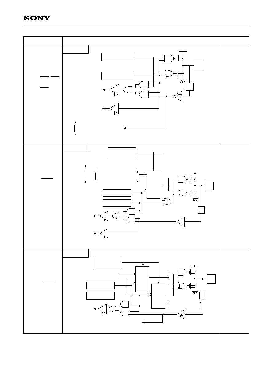
Input/Output Circuit Formats for Pins
PPO data
Internal data bus
Output becomes active from
high impedance by data writing
to port data register.
Ports A and B data
RD (Port A or Port B)
Port A
2 pins
2 pins
Hi-Z
Hi-Z
Hi-Z
After a reset
PB0/PPO8
PB2/PPO10
PB1/PPO9
PB3/PPO11
PA0/PPO0
to
PA7/PPO7
PB4/PPO12
to
PB7/PPO15
Port B
12 pins
Port B
Pin
Circuit format
Output becomes active from high
impedance by data writing to port
data register.
PPO9, PPO11 data
PB1, PB3 data
PPO9, PPO11 data
PPG control/status
register bit 0
Tri-state control
selection
RD (Port B)
Internal data bus
Output becomes active from high
impedance by data writing to port
data register.
Internal data bus
RD (Port B)
PB0, PB2 data
PPO8, PPO10 data
"0" after a reset
≠ 8 ≠
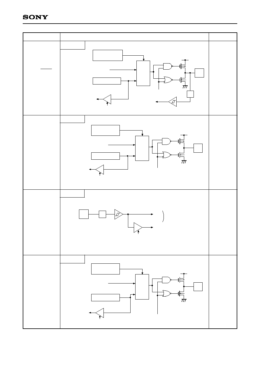
CXP88452/88460
PPO, RTO data
Port C direction
Port C data
IP
Input protection
circuit
Internal data bus
RD (Port C)
RD (Port C direction)
Internal data bus
"0" after a reset
6 pins
After a reset
PC0/PPO16
to
PC2/PPO18
PC5/RTO5
to
PC7/RTO7
Hi-Z
Pin
Circuit format
RTO3 data
Internal data bus
RD (Port C)
PC3 direction
PC3 data
IP
"0" after a reset
RTO4 data
RTG interruption
control register bit 7
Tri-state control
selection
RD (Port C)
PC4 direction
PC4 data
IP
RTO4 data
"0" after a reset
Internal data bus
Internal data bus
RD (Port C direction)
Internal data bus
RD (Port C direction)
"0" after a reset
Hi-Z
PC3/RTO3
Hi-Z
PC4/RTO4
1 pin
1 pin
Port C
Port C
≠ 9 ≠
CXP88452/88460
After a reset
Port D
Port D
Pin
Circuit format
Port D data
IP
Internal data bus
RD (Port D)
Port D direction
PD1: Remote control circuit
PD0: Interruption circuit
PD4, PD7: Serial CH0
Schmitt input
Internal data bus
RD (Port D direction)
"0" after a reset
PD2: 14-bit PWM
Timer/counter,
CTL duty detection circuit,
32kHz timer,
amplifier circuit
MPX
Port D data
IP
Internal data bus
RD (Port D)
Port D direction
Port D function
select
RD (Port D direction)
Internal data bus
PD3:
"0" after a reset
"0" after a reset
Hi-Z
PD0/INT1/NMI
PD1/RMC
PD4/CS0
PD7/SI0
Hi-Z
PD2/PWM
PD3/SRVO/
TO/DDO/
ADJ
4 pins
2 pins
MPX
Port D data
IP
Internal data bus
RD (Port D)
Port D direction
Port D function
select
MPX
SIO CH0
SIO CH0
Note)
PD5 is schmitt input
PD6 is inverter input
"0" after a reset
"0" after a reset
2 pins
PD5/SCK0
PD6/SO0
Hi-Z
Port D
≠ 10 ≠
CXP88452/88460
Internal data bus
RD (Port E)
DA gate output or
PWM output
Hi-Z control
MPX
Port E data
Port/DA/PWM
select
"1" after a reset
2 pins
PE6/PWM0/
DAA0
PE7/PWM1/
DAA1
High level
Port E
Internal data bus
RD (Port E)
SIO CH1
Hi-Z control
MPX
Port E data
Port E function
select
"1" after a reset
Internal data bus
RD (Port E)
SIO CH1
Hi-Z control
MPX
Port E data
Port/SCK
output select
IP
SIO CH1
"1" after a reset
Port E
Hi-Z
Hi-Z
Hi-Z
After a reset
PE0/SCK1
Port E
Port E
1 pin
1 pin
4 pins
PE1/SO1
PE2/SI1
PE3/SYNC
PE4/EXI0
PE5/EXI1
Pin
Circuit format
IP
RD (Port E)
Internal data bus
Schmitt input
PE2: SIO CH1
PE3
PE4 : Servo input
PE5
Note) For PE3/SYNC, CMOS schmitt input or TTL schmitt input can be selected
with the mask option.
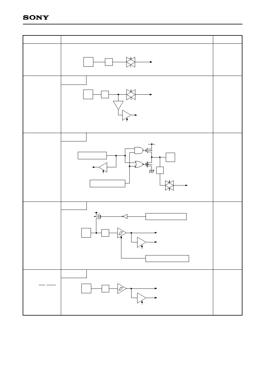
≠ 11 ≠
CXP88452/88460
4 pins
Hi-Z
Hi-Z
Hi-Z
After a reset
PF4/AN8
to
PF7/AN11
3 pins
AN0
to
AN3
4 pins
PF0/AN4
to
PF3/AN7
Pin
Circuit format
Port F data
IP
Internal data bus
RD (Port F)
Port/AD select
A/D converter
Input multiplexer
"1" after a reset
IP
Input multiplexer
A/D converter
Port F
RD (Port F)
Internal data bus
IP
Input multiplexer
A/D converter
Port F
Hi-Z
PG0/CFG
PG1/DFG
PG2/DPG
IP
RD (Port G)
Internal data bus
Schmitt input
Servo input
Schmitt width selection
Power ON/OFF control
Port G
3 pins
Hi-Z
PG3/EC/INT2
IP
RD (Port G)
Internal data bus
Schmitt input
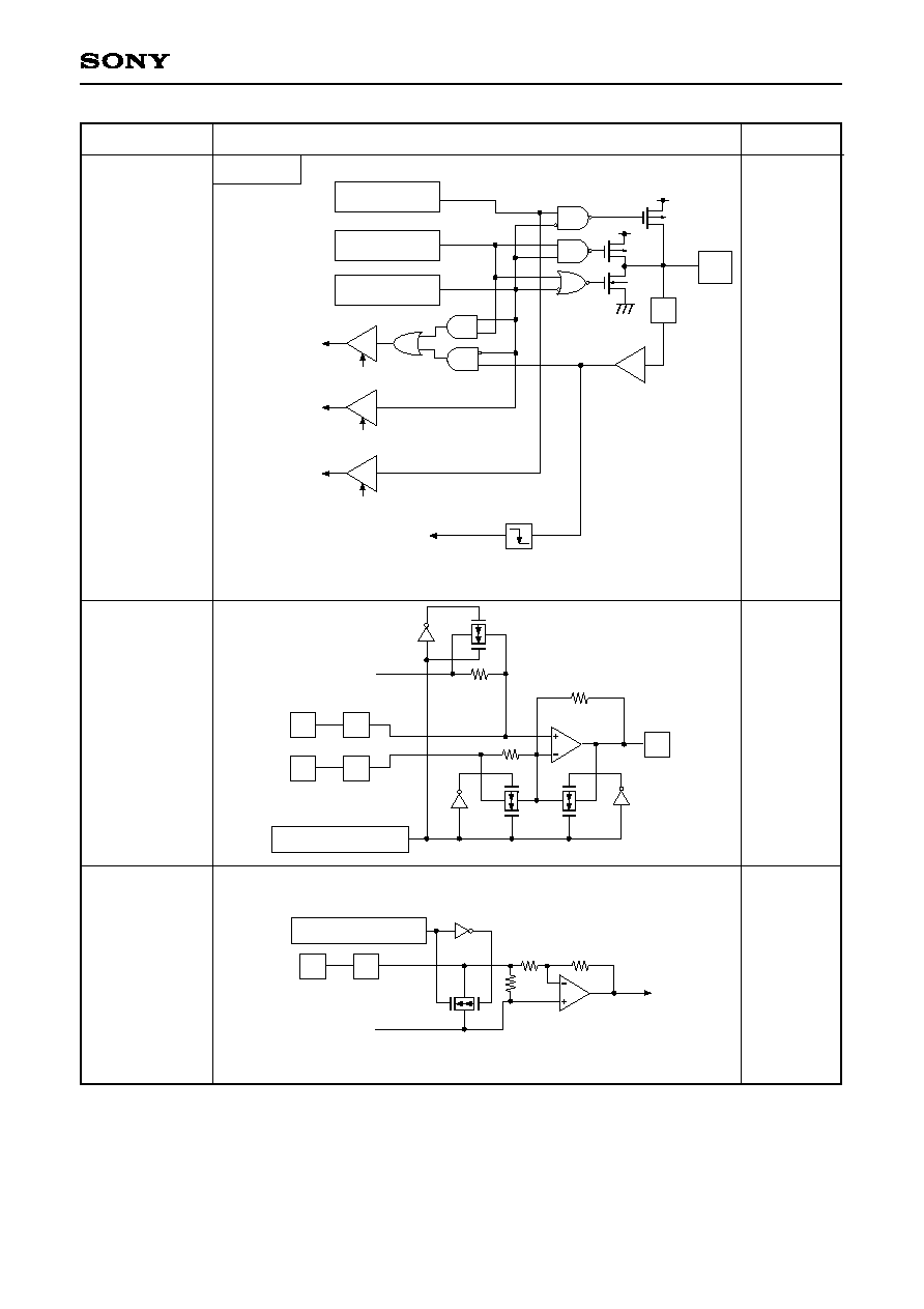
Port G
1 pin
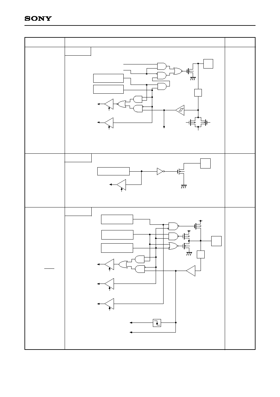
≠ 12 ≠
CXP88452/88460
Pin
After a reset
Circuit format
4 pins
Hi-Z
PH4 to PH7
Internal data bus
RD (Port H)
Port H data
12V drive voltage,
large current 12mA
Port H
4 pins
Hi-Z
PH0/SCL0
PH1/SCL1
PH2/SDA0
PH3/SDA1
SCL, SDA
Port H direction
Port H data
IP
Internal data bus
RD (Port H)
RD (Port H direction)
Internal data bus
I
2
C output enable
Schmitt input
Other serial interface
(CH2) pin)
SCL, SDA
(Serial interface
(CH2) circuit)
"0" after a reset
Port H
1 pin
Hi-Z
PI0/INT0
PI0 direction
PI0 data
Pull-up resistor
IP
Internal data bus
RD (Port I)
RD (Port I direction)
RD (pull-up resistor)
Internal data bus
Internal data bus
Standby release
Interruption circuit
Edge detection
Pull-up transistors approx. 100k
"0" after a reset
"0" after a reset
Port I
≠ 13 ≠
CXP88452/88460
Pin
After a reset
Circuit format
7 pins
Hi-Z
PI1 to PI7
Port I direction
Port I data
Pull-up resistor
IP
Internal data bus
RD (Port I)
RD (Port I direction)
RD (pull-up resistor)
Internal data bus
Internal data bus
Standby release
Edge detection
Pull-up transistors approx. 100k
"0" after a reset
"0" after a reset
Port I
Input pin charge control
IP
IP
CTLFAMPI (≠)
CTLFAMPI (+)
CTLFAMPO
CTLAGND
3 pins
1/2AMPV
DD
CTLFAMPI (+)
CTLFAMPI (≠)
CTLFAMPO
CTLSAMPI
1 pin
1/2AMPV
DD
Input pin charge control
IP
LPF circuit
CTLAGND
≠ 14 ≠
CXP88452/88460
IP
AMPV
SS
RTG control permission
RTO3
CTLHEAD (≠) pin
IP
HEADL (+) pin
Recording current control circuit
AMPV
SS
Write current select
RTG control permission
RTO6
RTO7
RTO3
AMPV
DD
1 pin
1 pin
Hi-Z
Hi-Z
Hi-Z
After a reset
CTLHEAD (+)
HEADL (≠)
CTLHEAD (≠)
1 pin
1 pin
Hi-Z
HEADL (+)
Pin
Circuit format
IP
AMPV
SS
RTG control permission
RTO3
CTLHEAD (+) pin
IP
HEADL (≠) pin
Recording current control circuit
AMPV
SS
Write current select
RTG control permission
RTO7
RTO6
RTO3
AMPV
DD
1 pin
1/2AMPV
DD
CTLAGND
AMPV
DD
IP
AMPV
SS
CTL AMP
≠ 15 ≠
CXP88452/88460
2 pins
Oscillation
Pin
After a reset
Circuit format
EXTAL
XTAL
IP
EXTAL
XTAL
∑ Shows the circuit composition
during oscillation.
∑ Feedback resistor is removed
and XTAL outputs High level
during stop.
2 pins
Oscillation
TEX
TX
IP
TEX
TX
∑ Shows the circuit
composition during
oscillation.
∑ Feedback resistor is
removed during 32kHz
oscillation circuit stop by
software. At that time,
TEX pin outputs Low level
and TX pin outputs High level.
32kHz
timer/counter
1 pin
Low level
(during a
reset)
RST
IP
Schmitt input
Pull-up resistor
OP
Mask option
2 pins
Hi-Z
RFG0
RFG1
IP
Comparator
Servo output
≠ 16 ≠
CXP88452/88460
1
AV
DD
should not exceed V
DD
+ 0.3V.
2
AMPV
DD
should not exceed V
DD
+ 0.3V.
3
V
IN
and V
OUT
should not exceed V
DD
+ 0.3V.
4
The large current output port is port H (PH7 to PH4).
Note) Usage exceeding absolute maximum ratings may permanently impair the LSI. Normal operation should
better take place under the recommended operating conditions. Exceeding those conditions may
adversely affect the reliability of the LSI.
Supply voltage
Input voltage
Output voltage
Medium drive output voltage
High level output current
High level total output current
Low level output current
Low level total output current
Operating temperature
Storage temperature
Allowable power dissipation
V
DD
AV
DD
AV
SS
AMPV
DD
AMPV
SS
V
IN
V
OUT
V
OUTP
I
OH
I
OH
I
OL
I
OLC
I
OL
Topr
Tstg
P
D
≠0.3 to +7.0
AVss to +7.0
1
≠0.3 to +0.3
AMPV
SS
to +7.0
2
≠0.3 to +0.3
≠0.3 to +7.0
3
≠0.3 to +7.0
3
≠0.3 to +15.0
≠5
≠50
15
20
130
≠20 to +75
≠55 to +150
600
V
V
V
V
V
V
V
V
mA
mA
mA
mA
mA
∞C
∞C
mW
Port H (PH7 to PH4) pin
Total of output pins
Other than large current output
ports (value per pin)
Large current output port
4
(value per pin)
Total of output pins
QFP package type
Item
Symbol
Rating
Unit
Remarks
Absolute Maximum Ratings
(Vss = 0V reference)
≠ 17 ≠
CXP88452/88460
Analog supply voltage
High level input voltage
Low level input voltage
Operating temperature
Supply voltage
5.5
5.5
5.5
5.5
5.5
5.5
V
DD
V
DD
V
DD
V
DD
+ 0.3
0.3V
DD
0.2V
DD
0.8
0.4
+75
V
V
V
V
V
V
V
V
V
V
∞C
V
Item
Symbol
Min.
Max.
Unit
Remarks
4.5
3.5
2.7
2.5
4.5
4.5
0.7V
DD
0.8V
DD
2.2
V
DD
≠ 0.4
0
0
0
≠0.3
≠20
AV
DD
AMPV
DD
V
IH
V
IHS
V
IHTS
V
IHEX
V
IL
V
ILS
V
ILTS
V
ILEX
Topr
Guaranteed operation range for 1/2 and 1/4
frequency dividing clock
Guaranteed operation range for 1/16 frequency
dividing clock or during sleep mode
Guaranteed operation range by TEX clock
Guaranteed data hold operation range
during stop
1
2
3
CMOS schmitt input
4
TTL schmitt input
5
EXTAL pin
6
TEX pin
7
3
CMOS schmitt input
4
TTL schmitt input
5
EXTAL pin
6
TEX pin
7
V
DD
1
AV
DD
and V
DD
should be set to the same voltage.
2
AMPV
DD
and V
DD
should be set to the same voltage.
3
Normal input port (each pin of PC, PD2, PD3, PD6, PF0 to PF3, PI1 to PI7 and PH0 to PH3), MP pin
4
Each pin of RST, PD0/INT1/NMI, PD1/RMC, PD4/CS0, PD5/SCK0, PD7/SI0, PE0/SCK1, PE2/SI1,
PE3/SYNC, PE4/EXI0, PE5/EXI1, PI0/INT0, PG3/EC/INT2 (For PE3/SYNC, when CMOS schmitt input is
selected with mask option.)
5
PE3/SYNC (when TTL schmitt input is selected with mask option.)
6
Specifies only during external clock input.
7
Specifies only during external event input.
Recommended Operating Conditions
(Vss = 0V reference)
≠ 18 ≠
CXP88452/88460
V
DD
= 4.5V, I
OH
= ≠0.5mA
V
DD
= 4.5V, I
OH
= ≠1.2mA
V
DD
= 4.5V, I
OL
= 1.8mA
V
DD
= 4.5V, I
OL
= 3.6mA
V
DD
= 4.5V, I
OL
= 12.0mA
V
DD
= 5.5V, V
IH
= 5.5V
V
DD
= 5.5V, V
IL
= 0.4V
V
DD
= 5.5V, V
IH
= 5.5V
High level
output voltage
4.0
3.5
0.5
≠0.5
0.1
≠0.1
≠1.5
V
V
V
V
V
µA
µA
µA
µA
µA
µA
µA
PH
EXTAL
TEX
RST
1
Item
Symbol
Pins
Conditions
Min.
V
DD,
V
SS
I
DD1
I
IZ
I
LOH
I
DDS1
I
DD2
I
DDS2
I
DDS3
V
OH
V
OL
I
IHE
I
ILE
I
IHT
I
ILT
I
ILR
Low level
output voltage
Input current
Typ.
0.4
0.6
1.5
40
≠40
10
≠10
≠400
±10
50
Max.
Unit
DC Characteristics (V
DD
= 4.5 to 5.5V)
Electrical Characteristics
(Ta = ≠20 to +75∞C, Vss = 0V reference)
V
DD
= 5.5V
3
Sleep mode
V
DD
= 5.5V
V
DD
= 5V ± 0.5V
Supply
current
2
V
DD
= 5.5V,
V
IL
= 0.4V
V
DD
= 5.5V,
V
I
= 0, 5.5V
V
DD
= 5.5V, V
OH
= 12V
V
DD
= 5.5V, V
OH
= 5.5V
16MHz crystal oscillation (C
1
= C
2
= 15pF)
Stop mode
(EXTAL and TEX pins oscillation stop)
I/O leakage
current
Open drain
output leakage
current (N-CH
Tr off state)
PA to PF,
PG3, PI, MP,
AN0 to AN3,
RST
1
PH4 to PH7
PH0 to PH3
37
2.1
58
9
50
8
100
35
10
mA
mA
µA
µA
µA
V
DD
= 3.3V
Sleep mode
V
DD
= 3V ± 0.3V
32kHz crystal oscillation (C
1
= C
2
= 47pF)
PA to PD,
PE0 to PE1,
PE6 to PE7,
PF4 to PF7,
PH (V
OL
only)
PI
10
µA

≠ 19 ≠
CXP88452/88460
1
RST pin specifies the input current when the pull-up resistor is selected, and specifies leakage current
when no resistor is selected.
2
When entire output pins are left open.
3
When setting upper 2 bits (CPU clock selection) of clock control register (CLC: 00FEh) to "00" and
operating in high speed mode (1/2 frequency dividing clock).
Item
Symbol
Pins
Conditions
Min.
Clock 1MHz
0V other than the measured pins
C
IN
Typ.
Max.
Unit
Input capacity
10
20
pF
PC, PD, PE0,
PE2 to PE5,
PF, PG, PI,
CTLHEAD (+),
CTLHEAD (≠),
CTLFAMPI (+),
CTLFAMPI (≠),
CTLSAMPI,
RFG,
XTAL, TEX
≠ 20 ≠
CXP88452/88460
TEX
EC
t
EH
t
EL
t
EF
t
ER
0.2V
DD
0.8V
DD
t
TH
t
TL
t
TF
t
TR
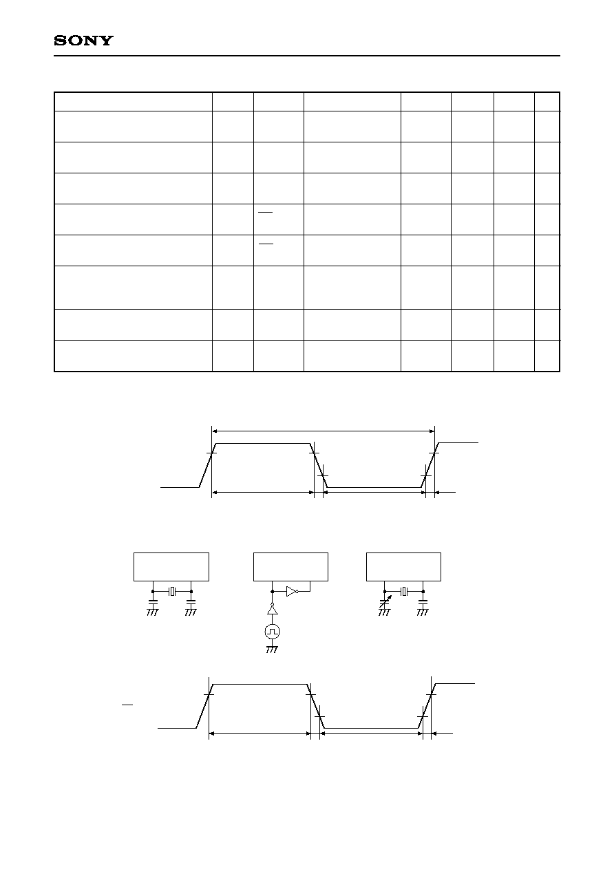
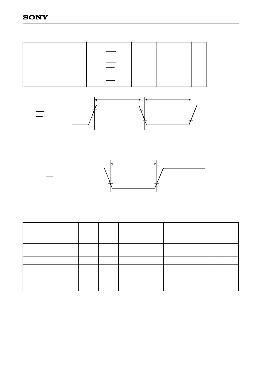
Fig. 3. Event count clock timing
1
t
sys indicates three values according to the contents of the clock control register (CLC; 00FEh) upper 2 bits
(CPU clock selection).
t
sys [ns] = 2000/fc (Upper 2 bits = "00"), 4000/fc (Upper 2 bits = "01"), 16000/fc (Upper 2 bits = "11")
EXTAL
XTAL
t
XH
t
XL
t
CF
t
CR
0.4V
V
DD ≠
0.4V
1/fc
External clock
EXTAL
XTAL
74HC04
Crystal oscillation
Ceramic oscillation
EXTAL
XTAL
C
1
C
2
32kHz clock applied condition
Crystal oscillation
TEX
TX
C
1
C
2
AC Characteristics
(1) Clock timing
System clock frequency
System clock input pulse width
System clock input rise and
fall times
Event count clock input
pulse width
Event count clock input
rise and fall times
System clock frequency
Event count clock input
pulse width
Event count clock input
rise and fall times
f
C
t
XL
,
t
XH
t
CR
,
t
CF
t
EH
,
t
EL
t
ER
,
t
EF
f
C
t
TL
,
t
TH
t
TR
,
t
TF
XTAL
EXTAL
XTAL
EXTAL
XTAL
EXTAL
EC
EC
TEX
TX
TEX
TEX
MHz
ns
ns
ns
ms
kHz
µs
ms
Item
Symbol
Pins
Conditions
Unit
Fig. 1, Fig. 2
Fig. 1, Fig. 2
External clock drive
Fig. 1, Fig. 2
External clock drive
Fig. 3
Fig. 3
V
DD
= 2.7 to 5.5V
Fig. 2 (32kHz clock
applied condition)
Fig. 3
Fig. 3
Typ.
32.768
Min.
1
28
t
sys
+
200
1
10
Max.
16
200
20
20
(Ta = ≠20 to +75∞C, V
DD
= 4.5 to 5.5V, Vss = 0V reference)
Fig. 1. Clock timing
Fig. 2. Clock applied condition
≠ 21 ≠
CXP88452/88460
Input mode
Output mode
Input mode
Output mode
SCK0 input mode
SCK0 output mode
SCK0 input mode
SCK0 output mode
SCK0 input mode
SCK0 output mode
Chip select transfer mode
(SCK0 = output mode)
Chip select transfer mode
(SCK0 = output mode)
Chip select transfer mode
Chip select transfer mode
Chip select transfer mode
Note 1)
t
sys indicates three values according to the contents of the clock control register (CLC; 00FEh) upper
2 bits (CPU clock selection).
t
sys [ns] = 2000/fc (Upper 2 bits = "00"), 4000/fc (Upper 2 bits = "01"), 16000/fc (Upper 2 bits = "11")
Note 2) The load of SCK0 output mode and SO0 output delay time is 50pF + 1TTL.
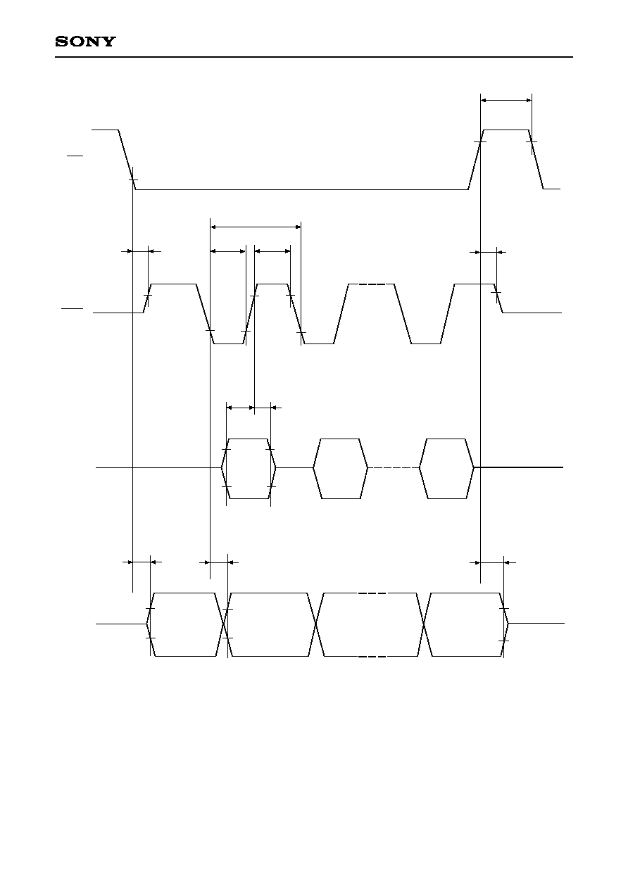
(2) Serial transfer (CH0)
(Ta = ≠20 to +75∞C, V
DD
= 4.5 to 5.5V, Vss = 0V reference)
Item
CS0
SCK0
delay time
CS0
SCK0
floating delay time
CS0
SO0
delay time
CS0
SO0
floating delay time
CS0
high level width
SCK0
cycle time
SCK0
high and low level widths
SI0 input set-up time
(against SCK0
)
SI0 input hold time
(against SCK0
)
SCK0
SO0 delay time
t
DCSK
t
DCSKF
t
DCSO
t
DCSOF
t
WHCS
t
KCY
t
KH
t
KL
t
SIK
t
KSI
t
KSO
SCK0
SCK0
SO0
SO0
CS0
SCK0
SCK0
SI0
SI0
SO0
ns
ns
ns
ns
ns
Symbol
Pins
Min.
t
sys + 200
t
sys + 200
t
sys + 200
t
sys + 200
t
sys + 200
2
t
sys + 200
16000/fc
t
sys + 100
8000/fc ≠ 100
≠
t
sys + 100
200
2
t
sys + 100
100
ns
ns
ns
ns
ns
ns
ns
ns
ns
ns
2
t
sys + 100
100
Max.
Unit
Conditions
≠ 22 ≠
CXP88452/88460
Fig. 4. Serial transfer timing (CH0)
CS0
SCK0
0.2V
DD
0.8V
DD
t
WHCS
t
DCSK
t
DCSKF
0.8V
DD
0.2V
DD
0.8V
DD
t
KCY
t
KL
t
KH
0.8V
DD
0.2V
DD
SI0
t
SIK
t
KSI
Input data
t
DCSO
t
KSO
t
DCSOF
Output data
0.8V
DD
0.2V
DD
SO0
≠ 23 ≠
CXP88452/88460
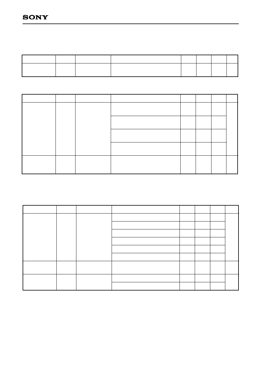
Serial transfer (CH1) (SIO mode)
(Ta = ≠20 to +75∞C, V
DD
= 4.5 to 5.5V, Vss = 0V reference)
Item
Symbol
Pins
Min.
Max.
Unit
Conditions
SCK1 cycle time
SCK1 high and low
level widths
SI1 input setup time
(for SCK1
)
SI1 input hold time
(for SCK1
)
SCK1
SO1 delay time
t
KCY
t
KH
t
KL
t
SIK
t
KSI
t
KSO
SCK1
SCK1
SI1
SI1
SO1
Input mode
Output mode
Input mode
Output mode
SCK1 input mode
SCK1 output mode
SCK1 input mode
SCK1 output mode
SCK1 input mode
SCK1 output mode
2
t
sys + 200
16000/fc
t
sys +100
8000/fc ≠ 50
100
200
t
sys + 200
100
t
sys + 200
100
ns
ns
ns
ns
ns
ns
ns
ns
ns
ns
Note 1)
t
sys indicates three values according to the contents of the clock control register (CLC: 00FEh) upper
2 bits (CPU clock selection).
t
sys [ns] = 2000/fc (Upper 2 bits = "00"), 4000/fc (Upper 2 bits = "01"), 16000/fc (Upper 2 bits = "11")
Note 2) The load of SCK1 output mode and SO1 output delay time is 50pF + 1TTL.
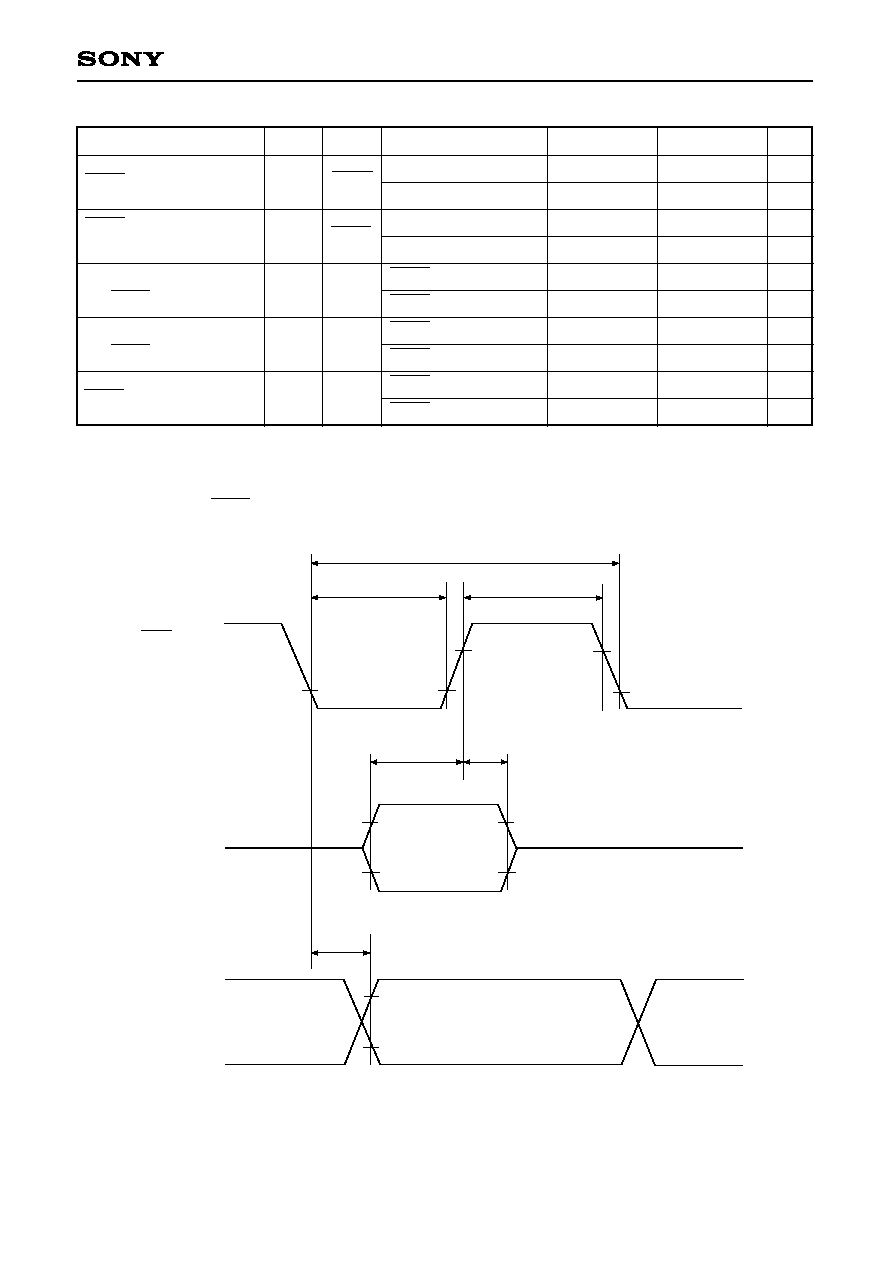
Fig. 5. Serial transfer CH1 timing (SIO mode)
SCK1
SI1
SO1
t
KCY
t
KL
t
KH
0.2V
DD
0.8V
DD
t
SIK
t
KSI
t
KSO
Input data
Output data
0.2V
DD
0.8V
DD
0.2V
DD
0.8V
DD
≠ 24 ≠
CXP88452/88460
SO1 cycle time
SI1 data setup time
SI1 data hold time
t
LCY
t
LSU
t
LHD
SO1
SI1
SI1
SI1
1
2
2
104
µs
µs
µs
Item
Symbol
Pins
Conditions
Min.
Typ.
Max.
Unit
Serial transfer (CH1) (Special mode) (Ta = ≠20 to +75∞C, V
DD
= 4.5 to 5.5V, Vss = 0V reference)
1
t
LCY
is specified only when serial mode register (CH1) (SIOM1: 05F2h) lower 2 bits (SO1 clock selection)
are set at 104µs.
Note) The load of SO1 pin is 50pF + 1TTL.
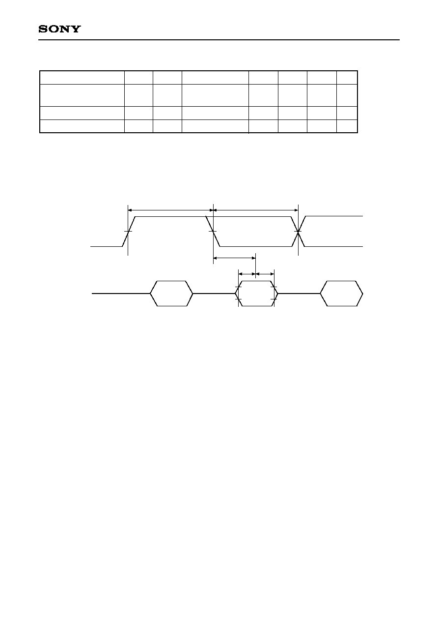
Fig. 6. Serial transfer CH1 timing (Special mode)
SO1
SI1
t
LCY
Start bit
Output data bit
t
LCY
0.5V
DD
0.8V
DD
0.2V
DD
t
LCY/2
t
LSU
t
LHD
Input
data bit
≠ 25 ≠
CXP88452/88460
Serial transfer (CH2)
(Ta = ≠20 to +75∞C, V
DD
= 4.5 to 5.5V, Vss = 0V reference)
Item
SCL clock frequency
Bus-free time before starting transfer
Hold time for starting transfer
Clock low level width
Clock high level width
Setup time for repeated transfers
Data hold time
Data set-up time
SDA, SCL rise time
SDA, SCL fall time
Setup time for transfer completion
f
SLC
t
BUF
t
HD; STA
t
LOW
t
HIGH
t
SU; STA
t
HD; DAT
t
SU; DAT
t
R
t
F
t
SU; STO
SCL
SDA, SCL
SDA, SCL
SCL
SCL
SDA, SCL
SDA, SCL
SDA, SCL
SDA, SCL
SDA, SCL
SDA, SCL
2.6
1.0
1.0
1.0
1.0
0
1
100
1.6
400
300
300
kHz
µs
µs
µs
µs
µs
µs
ns
ns
ns
µs
Symbol
Pins
Conditions
Min.
Max.
Unit
1
The SCL fall time (300ns Max.) is not included in the data hold time.
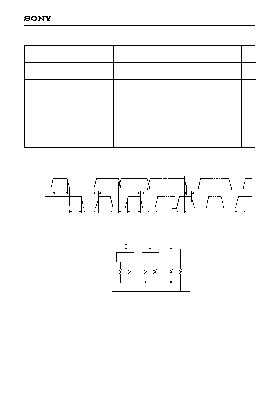
Fig. 7. Serial transfer timing (CH2)
P
St
t
SU; STO
t
SU; STA
t
HD; STA
t
SU; DAT
t
HIGH
t
HD; DAT
t
F
t
R
t
LOW
t
HD; STA
S
P
t
BUF
SDA
SCL
Fig. 8. Device recommended circuit
Device
Device
R
S
R
S
R
S
R
S
R
P
R
P
SDA0
(or SDA1)
SCL0
(or SCL1)
∑ A pull-up resistor (R
P
) must be connected to SDA0 (or SDA1) and SCL0 (or SCL1).
∑ The SDA0 (or SDA1) and SCL0 (or SCL1) series resistance (Rs = 300
or less) can be used to reduce the
spike noise caused by CRT flashover.
≠ 26 ≠
CXP88452/88460
Conversion time
Sampling time
Reference input voltage
Analog input voltage
t
CONV
t
SAMP
V
REF
V
IAN
Ta = 25∞C
V
DD
= AV
DD
= AV
REF
= 5.0V
V
SS
= AV
SS
= 0V
Operating mode
Sleep mode
Stop mode
32kHz operating mode
Linearity error
Absolute error
Resolution
AV
REF
current
AV
REF
I
REF
µs
µs
V
V
AV
DD
AV
REF
1.0
mA
10
µA
0.6
160/f
ADC
1
12/f
ADC
1
AV
DD
≠ 0.5
0
Item
Symbol
Pins
Conditions
Min.
Typ.
Max.
Unit
Bits
(4) A/D converter characteristics
(Ta = ≠20 to +75∞C, V
DD
= AV
DD
= 4.5 to 5.5V, AV
REF
= 4.0 to AV
DD
, Vss = AV
SS
= 0V reference)
8
±1
±2
LSB
LSB
Analog input
Linearity error
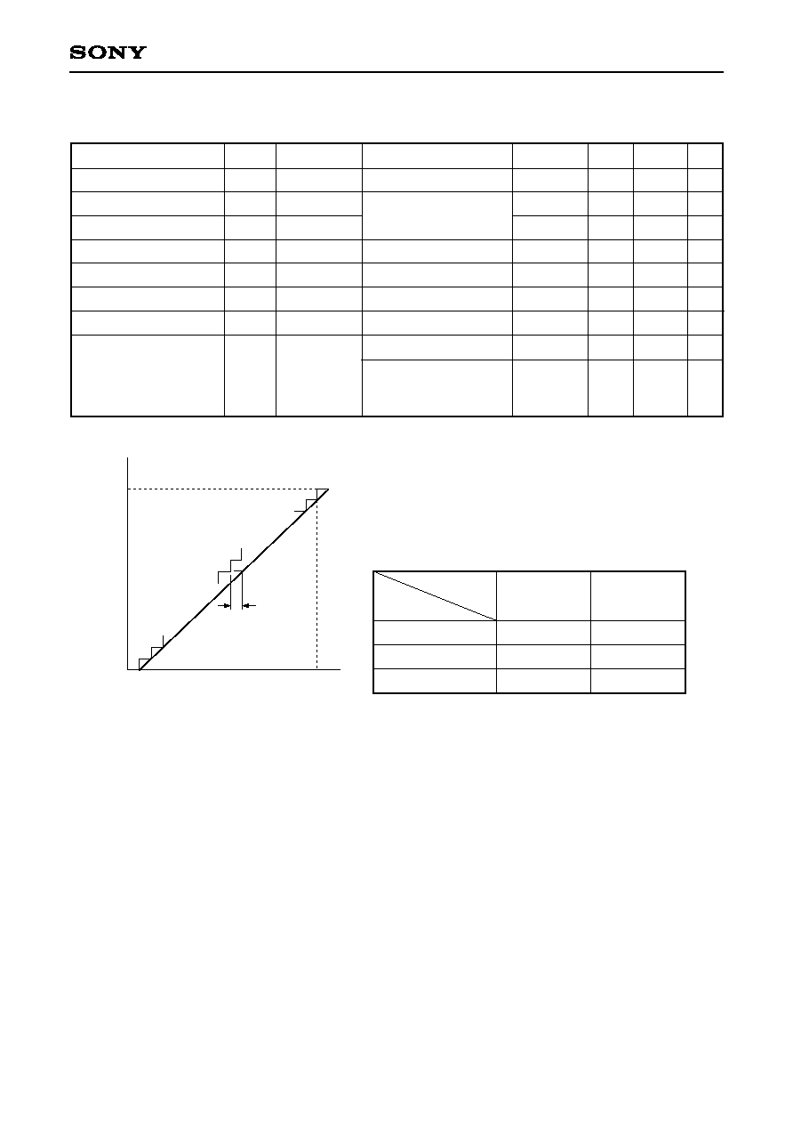
00h
01h
FEh
FFh
D
i
g
i
t
a
l
c
o
n
v
e
r
s
i
o
n
v
a
l
u
e
V
ZT
V
FT
Fig. 9. Definitions of A/D converter terms
AN0 to AN7
AV
REF
1
f
ADC
indicates the below values due to the peripheral
clock control register (PCC: 05F8h) bit 3 and clock control
register (CLC: 00FEh) upper 2 bits.
ADCCK
PCK1, PCK0
00 (
= f
EX
/2)
01 (
= f
EX
/4)
11 (
= f
EX
/16)
f
ADC
= fc/2
f
ADC
= fc/4
f
ADC
= fc/16
f
ADC
= fc
f
ADC
= fc/2
f
ADC
= fc/8
0 (
/2 selection) 1 (
selection)
≠ 27 ≠
CXP88452/88460
(5) Others
(Ta = ≠20 to +75∞C, V
DD
= 4.5 to 5.5V, Vss = 0V reference)
Item
CFG input
high and low level widths
DFG input
high and low level widths
DPG minimum pulse width
DPG minimum
removal time
EXI input
high and low level widths
t
CFH
t
CFL
t
DFH
t
DFL
t
DPW
t
rem
t
EIH
t
EIL
CFG
DFG
DPG
DPG
EXI0
EXI1
ns
ns
ns
ns
ns
Symbol
Pins
Min.
24
t
FRC
+ 200
16
t
FRC
+ 200
8
t
FRC
+ 200
16
t
FRC
+ 200
8
t
FRC
+ 200 +
t
sys
Max.
Unit
t
sys = 2000/fc
Conditions
Note 1)
t
FRC
= 1000/fc [ns]
Note 2)
t
sys indicates three values according to the contents of the clock control register (CLC: 00FEh)
upper 2 bits (CPU clock selection).
t
sys [ns] = 2000/fc (Upper 2 bits = "00"), 4000/fc (Upper 2 bits = "01"), 16000/fc (Upper 2 bits = "11")
External interruption high and
low level widths
Reset input low level width
INT0
INT1
INT2
NMI
PI0 to PI7
RST
1
32/fc
µs
µs
Item
Symbol
Pins
Conditions
Min.
Max.
Unit
t
IH
t
IL
t
RSL
(4) Interruption, reset input
(Ta = ≠20 to +75∞C, V
DD
= 4.5 to 5.5V, Vss = 0V reference)
0.2V
DD
0.8V
DD
t
IH
t
IL
INT0
INT1
INT2
NMI
PI0 to PI7
(During standby release input)
(Falling edge)
Fig. 10. Interruption input timing
t
RSL
0.2V
DD
RST
Fig. 11. Reset input timing
≠ 28 ≠
CXP88452/88460
0.8V
DD
CFG
t
CFH
t
CFL
0.2V
DD
0.8V
DD
DFG
t
DFH
t
DFL
0.2V
DD
0.8V
DD
t
DPW
t
rem
DPG
0.8V
DD
EXI0
EXI1
t
EIH
t
EIL
0.2V
DD
t
rem
Fig. 12. Other timings
≠ 29 ≠
CXP88452/88460
Voltage gain
1
Output offset
voltage
LPF cut-off
frequency
Item
Symbol
Pins
Conditions
Min.
Typ.
Max.
Unit
dB
mV
kHz
(3) CTL 2nd amplifier characteristics
(AMPV
DD
= V
DD
= 5.0V, AMPV
SS
= Vss = 0V, Ta = ≠20 to +75∞C)
Gain = 5dB
Gain = 8dB
Gain = 11dB
Gain = 14dB
Gain = 17dB
Gain = 20dB
CTLSAMPI = open,
Gain = 5dB
12kHz, f
DC
≠ 3dB
20kHz, f
DC
≠ 3dB
A
VCTL2
V
OSCTL2
F
CCTL
CTLSAMPI
CTLSAMPI
CTLSAMPI
3.5
6.2
9.0
12.0
15.0
18.0
≠30
8
12
5.5
8.2
11.0
14.0
17.0
20.0
0
12
20
7.5
10.2
13.0
16.0
19.0
22.0
+30
24
42
Voltage gain
1
Output offset
voltage
Item
Symbol
Pins
Conditions
Min.
Typ.
Max.
Unit
dB
mV
(2) CTL 1st amplifier characteristics
(AMPV
DD
= V
DD
= 5.0V, AMPV
SS
= Vss = 0V, Ta = ≠20 to +75∞C)
CTLFAMPI (≠) = 0V,
Gain = 16dB
CTLFAMPI (≠) = 0V,
Gain = 34dB
CTLFAMPI (≠) = 0V,
Gain = 49dB
CTLFAMPI (≠) = 0V,
Gain = 55dB
CTLFAMPI (≠),
CTLFAMPI (+) = open,
Gain = 16dB
A
VCTL1
V
OSCTL1
CTLFAMPI (≠)
CTLFAMPI (+)
CTLFAMPI (≠)
CTLFAMPI (+)
13.5
31.8
46.5
52.5
≠25
15.5
33.8
48.5
54.5
0
17.5
35.8
50.5
56.5
+25
1
The result after monitoring CTLFAMPO pin when the electrolytic capacitor (10µF) is connected to
CTLFAMP (≠) and CTLFAMP (+).
Reference level
output voltage
V
OR
CTLAGND
Item
Symbol
Pins
Conditions
Min.
Typ.
Max.
Unit
V
(AMPV
DD
= V
DD
= 5.0V, AMPV
SS
= Vss = 0V, Ta = ≠20 to +75∞C)
2.75
2.20
2.45
Analog Circuit Characteristics
(1) Amplifier circuit reference voltage characteristics
≠ 30 ≠
CXP88452/88460
1
The result after monitoring ANOUT pin when the electrolytic capacitor (10µF) is connected to CTLSAMPI.
2
The reference value of the comparator level is CTLAGND.
Voltage gain
3
Input sensitivity
Item
Symbol
Pins
Conditions
Min.
Typ.
Max.
Unit
dB
µVp-p
(4) CTL amplifier characteristics (CTL1stAMP + CTL2ndAMP)
(AMPV
DD
= V
DD
= 5.0V, AMPV
SS
= Vss = 0V, Ta = ≠20 to +75∞C)
CTLHEAD (≠) = 0V,
Gain = (16dB + 5dB)
CTLHEAD (≠) = 0V,
Gain = (55dB + 20dB)
CTLHEAD (≠) = 0V,
Gain = (55dB + 20dB)
Comparator = ±150mV
0-p
A
VCTL
V
SCTL
CTLHEAD (≠)
CTLHEAD (+)
CTLHEAD (≠)
CTLHEAD (+)
17.0
70.5
60
20.5
74.5
70
23.5
77.0
140
3
The result when waveform is input from CTLHEAD (+) pin and ANOUT pin is monitored after performing
coupling electrolytic capacitor (10µF) of CTLHEAD (≠) and CTLHEAD (+), and coupling electrolytic capacitor
(10µF) of HEADL (≠) and HEADL (+), CTLFAMPI (≠) and CTLFAMPI (+) , and CTLFAMPO and CTLSAMPI.
Gain is maximum ≠1.5dB lowered when waveform is input from CTLHEAD (+) pin.
Comparator
level
2
Item
Symbol
Pins
Conditions
Min.
Typ.
Max.
Unit
mV
Comparator level = +100mV
0-p
Comparator level = +150mV
0-p
Comparator level = +200mV
0-p
Comparator level = +250mV
0-p
Comparator level = +300mV
0-p
Comparator level = +400mV
0-p
Comparator level = +500mV
0-p
Comparator level = +600mV
0-p
Comparator level = +1000mV
0-p
Comparator level = ≠100mV
0-p
Comparator level = ≠150mV
0-p
Comparator level = ≠200mV
0-p
Comparator level = ≠250mV
0-p
Comparator level = ≠300mV
0-p
Comparator level = ≠400mV
0-p
Comparator level = ≠500mV
0-p
Comparator level = ≠600mV
0-p
Comparator level = ≠1000mV
0-p
V
CCTL
CTLSAMPI
80
110
160
210
250
340
420
530
850
≠90
≠110
≠150
≠200
≠240
≠340
≠430
≠540
≠870
110
150
200
250
290
380
470
570
920
≠120
≠130
≠190
≠240
≠280
≠380
≠480
≠580
≠970
140
190
240
290
330
420
520
610
990
≠150
≠190
≠230
≠280
≠320
≠420
≠530
≠620
≠1070
≠ 31 ≠
CXP88452/88460
ATC peak hold circuit
initialize voltage value
2
ATC comparator level
offset voltage
3
Item
Symbol
Pins
Conditions
Min.
Typ.
Max.
Unit
mV
mV
(6) Auto threshold control circuit (ATC) characteristics
(AMPV
DD
= V
DD
= 5.0V, AMPV
SS
= Vss = 0V, Ta = ≠20 to +75∞C)
Voltage = ≠150mV
0-P
Voltage = ≠400mV
0-P
Gain = 1/6 (16.7%)
Gain = 1/5 (20%)
Gain = 1/4 (25%)
Gain = 1/3 (33.3%)
Gain = 2/5 (40%)
Gain = 1/2 (50%)
Gain = 3/5 (60%)
V
ATCINIT
V
ATCOFF
≠110
≠350
≠150
≠400
≠70
≠90
≠90
≠70
≠90
≠70
≠90
≠190
≠450
≠160
≠210
≠210
≠160
≠210
≠160
≠210
2
Reference is CTLAGND.
3
Reference is CTLAGND.
When comparator level is generated using ATC, actual comparator level is as follows by the offset voltage
inside of ATC.
Vin
◊
gain + |offset voltage|
Example: Gain = 1/2
Vin
◊
1/2 + 160
RTG schmitt width
CFG/DFG/DPG
Item
Symbol
Pins
Conditions
Min.
Typ.
Max.
Unit
mV
mV
(7) Schmitt characteristics
(AMPV
DD
= V
DD
= 5.0V, AMPV
SS
= Vss = 0V, Ta = ≠20 to +75∞C)
Schmitt width 1Vp-p
Schmitt width 410mVp-p
Schmitt width 1Vp-p
S
RFG
RFG0,
RFG1
S
CFG
S
DFG
S
DPG
CFG,
DFG,
DPG
820
180
700
920
300
900
1020
420
1100
Write current
1
Item
Symbol
Pins
Conditions
Min.
Typ.
Max.
Unit
mA
(5) RECCTL write circuit characteristics
(AMPV
DD
= V
DD
= 5.0V, AMPV
SS
= Vss = 0V, Ta = ≠20 to +75∞C)
Write current 2.0mAp-p
Write current 3.0mAp-p
Write current 4.0mAp-p
Write current 5.0mAp-p
Write current 6.0mAp-p
Write current 7.0mAp-p
Write current 8.0mAp-p
Write current 9.0mAp-p
Write current 10.0mAp-p
I
OREC
CTLHEAD (≠)
CTLHEAD (+)
0.8
1.4
2.0
2.4
3.0
3.5
4.5
5.0
5.5
1.8
2.8
3.8
4.8
6.0
6.8
7.8
8.8
7.7
3.6
5.0
7.0
8.5
10.0
11.5
13.0
15.0
17.0
1
The current which flows when CTLHEAD (≠) and CTLHEAD (+) shorts.
≠ 32 ≠
CXP88452/88460
Appendix
EXTAL
XTAL
C
1
C
2
Rd
(i)
TEX
TX
C
1
C
2
Rd
(ii)
Manufacturer
RIVER
ELETEC
CO., LTD.
KINSEKI LTD.
Model
HC-49/U03
HC-49/U (-S)
P3
fc (MHz)
8.00
10.00
12.00
8.00
10.00
16.00
12
12
10
5
16 (12)
16 (12)
10
16.00
5
16 (12)
16 (12)
0
0
C
1
(pF)
C
2
(pF)
Rd (
)
Circuit
example
(i)
(i)
470k
(ii)
Mask option table
12.00
12
12
32.768kHz
18
30
1
The input circuit format can be selected for PE3/SYNC pin.
Item
Content
Reset pin pull-up resistor
Input circuit format
1
Non-existent
CMOS schmitt
Existent
TTL schmitt
Fig. 13. Recommended oscillation circuit
≠ 33 ≠
CXP88452/88460
0
2
3
4
5
6
0.01
(10µA)
0.1
(100µA)
1
10
100
0
5
10
15
I
DD
vs. V
DD
(fc = 16MHz, Ta = 25∞C, W
0
9)
I
D
D
≠
S
u
p
p
l
y
c
u
r
r
e
n
t
[
m
A
]
V
DD ≠
Supply voltage [V]
32kHz
Sleep mode
I
DD
vs. fc
(V
DD
= 5.0V, Ta = 25∞C, W
0
9)
fc
≠
System clock [MHz]
Sleep mode
1/16 dividing mode
1/2 dividing mode
1/2 dividing mode
1/4 dividing mode
1/16 dividing mode
Sleep mode
1/4 dividing mode
32kHz mode
I
D
D
≠
S
u
p
p
l
y
c
u
r
r
e
n
t
[
m
A
]
40
20
10
0
30
Characteristics Curve
≠ 34 ≠
CXP88452/88460
Package Outline
Unit: mm
SONY CODE
EIAJ CODE
JEDEC CODE
PACKAGE MATERIAL
LEAD TREATMENT
LEAD MATERIAL
PACKAGE MASS
EPOXY RESIN
SOLDER PLATING
42/COPPER ALLOY
PACKAGE STRUCTURE
23.9 ± 0.4
QFP-100P-L01
100PIN QFP (PLASTIC)
20.0 ≠ 0.1
+ 0.4
0.15 ≠ 0.05
+ 0.1
1
5
.
8
±
0
.
4
1
7
.
9
±
0
.
4
1
4
.
0
≠
0
.
1
+
0
.
4
2.75 ≠ 0.15
+ 0.35
A
0.65
M
0.13
QFP100-P-1420
1.7g
1
100
81
80
51
50
31
30
0.3 ≠ 0.1
+ 0.15
DETAIL A
0∞ to 10∞
0
.
8
±
0
.
2
(
1
6
.
3
)
0.15
0.1 ≠ 0.05
+ 0.2